ST STM32H5 User manual

Introduction
The STM32H5 Nucleo-64 board based on the MB1814 reference board (order code NUCLEO-H503RB) provides an affordable
and flexible way for users to try out new concepts and build prototypes, by choosing from the various combinations of
performance and power consumption features provided by the STM32H5 series microcontroller.
The ARDUINO® Uno V3 connectivity and the ST morpho headers provide easy expansion of the functionality of the STM32
Nucleo open development platform with a wide choice of specialized shields.
The STM32H5 Nucleo-64 board does not require any separate probe as it integrates the STLINK-V3EC debugger/programmer.
The STM32H5 Nucleo-64 board comes with the STM32 comprehensive free software libraries and examples available with the
STM32CubeH5 MCU Package.
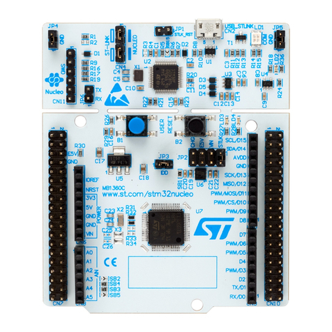
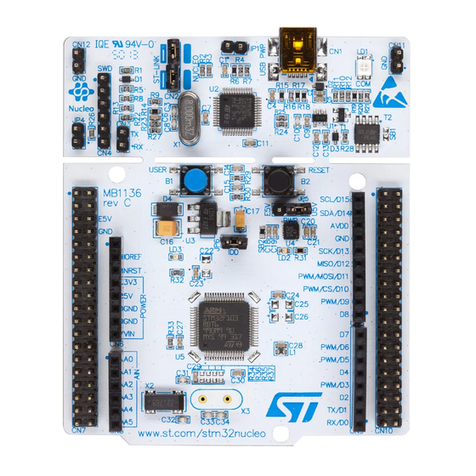
Figure 1. NUCLEO-H503RB top view Figure 2. NUCLEO-H503RB bottom view
Pictures are not contractual.
STM32H5 Nucleo-64 board (MB1814)
UM3121
User manual
UM3121 - Rev 1 - February 2023
For further information contact your local STMicroelectronics sales office. www.st.com

1Features
•NUCLEO-H503RB microcontroller based on the Arm® Cortex®-M33 core, featuring 128 Kbytes of flash
memory and 32 Kbytes of SRAM in an LQFP64 package
• USB Type-C® (Device mode/Full speed)
• One user LED shared with ARDUINO® Uno V3
• Reset and user push-buttons
• 32.768 kHz LSE crystal oscillator
• 24 MHz HSE crystal oscillator
• Board connectors:
–ST-LINK USB Type-C®
–User USB Type-C®
– MIPI10 for debugging (SWD/JTAG)
–ARDUINO® Uno V3 expansion connector
– ST morpho extension pin headers for full access to all STM32 I/Os
• Flexible power-supply options: ST-LINK USB VBUS, user USB connector, or external sources
• On-board STLINK-V3EC debugger/programmer with USB re-enumeration capability: mass storage, Virtual
COM port, and debug port
• Comprehensive free software libraries and examples available with the STM32CubeH5 MCU Package
• Support of a wide choice of Integrated Development Environments (IDEs) including IAR Embedded
Workbench®, MDK-ARM, and STM32CubeIDE
Note: Arm is a registered trademark of Arm Limited (or its subsidiaries) in the US and/or elsewhere.
UM3121
Features
UM3121 - Rev 1 page 2/37

2Ordering information
To order the STM32H5 Nucleo-64 board, refer to Table 1. Additional information is available from the datasheet
and reference manual of the target STM32.
Table 1. Ordering information
Order code Board reference Target STM32
NUCLEO-H503RB MB1814 STM32H503RBT6
2.1 Products and codification
The meaning of the codification is explained in Table 2.
Table 2. Codification explanation
NUCLEO-XXYYRT Description Example: NUCLEO-H503RB
XX MCU series in STM32 32‑bit Arm Cortex MCUs STM32H5 series
YY MCU product line in the series STM32H503
R STM32 package pin count 64 pins
TSTM32 flash memory size:
• B for 128 Kbytes 128 Kbytes
In this document, for any information that is common to all sales types, the references are noted as the STM32H5
Nucleo-64 board.
UM3121
Ordering information
UM3121 - Rev 1 page 3/37

3Development environment
3.1 System requirements
• Multi‑OS support: Windows® 10, Linux® 64-bit, or macOS®
• USB Type-A or USB Type-C® to USB Type-C® cable
Note: macOS® is a trademark of Apple Inc., registered in the U.S. and other countries and regions.
Linux® is a registered trademark of Linus Torvalds.
Windows is a trademark of the Microsoft group of companies.
3.2 Development toolchains
•IAR Systems® - IAR Embedded Workbench®(1)
•Keil® - MDK-ARM(1)
• STMicroelectronics - STM32CubeIDE
1. On Windows® only.
UM3121
Development environment
UM3121 - Rev 1 page 4/37

4Conventions
Table 3 provides the conventions used for the ON and OFF settings in the present document.
Table 3. ON/OFF convention
Convention Definition
Jumper JPx ON Jumper fitted
Jumper JPx OFF Jumper not fitted
Jumper JPx [1-2] Jumper fitted between Pin 1 and Pin 2
Solder bridge SBx ON SBx connections closed by 0 Ω resistor
Solder bridge SBx OFF SBx connections left open
Resistor Rx ON Resistor soldered
Resistor Rx OFF Resistor not soldered
Capacitor Cx ON Capacitor soldered
Capacitor Cx OFF Capacitor not soldered
UM3121
Conventions
UM3121 - Rev 1 page 5/37

5Quick start
The STM32H5 Nucleo-64 board is a low-cost and easy-to-use development kit, to evaluate and start development
quickly with an STM32H5 series microcontroller in an LQFP 64-pin package.
Before installing and using the product, accept the Evaluation Product License Agreement from the www.st.com/
epla webpage. For more information on the STM32H5 Nucleo-64 board and demonstration software, visit the
www.st.com/stm32nucleo webpage.
5.1 Getting started
Follow the sequence below to configure the STM32H5 Nucleo-64 board and launch the demonstration application
(refer to Figure 5 for component location):
1. Check the jumper position on the board (refer to Figure 3).
2. Power the board by connecting the STM32H5 Nucleo-64 board to a PC with a USB cable (USB Type-A to
USB Type-C® or USB Type-C® to USB Type-C®) through the USB connector (CN1) of the board.
3. Then, the 5V_PWR green (LD3), the COM (LD1), and the PWR (LD7) LEDs light up, and the user green
LED (LD2) blinks.
4. Press the user blue button (B1).
5. Observe how the blinking of the green LED (LD2) changes according to the clicks on the button (B1).
6. The demonstration software and several software examples that allow exercising Nucleo features are
available on the www.st.com website.
7. Develop your application using the available examples.
5.2 Default board configuration
The default jumper configuration and voltage settings are shown in Table 4.
Table 4. Default jumper configuration
Jumper Definition Position Comment
JP1 ST-LINK reset OFF STLINK-V3EC MCU is not under Reset
mode
JP2 IDD measurement ON VDD_MCU current measurement
JP5 5 V power source selection [1-2] 5 V from STLINK-V3EC (5V_STLK)
JP6 VDD ON VDD supplied with 3V3
UM3121
Quick start
UM3121 - Rev 1 page 6/37
Two additional jumpers are set on the GND header (CN11 and CN12) as spare jumpers for configuration usage
(JP1).
Figure 3. Default jumper settings
DT59073V1
JP5
JP6
JP2
UM3121
Default board configuration
UM3121 - Rev 1 page 7/37

6Hardware layout and configuration
The STM32H5 Nucleo-64 board is designed around an STM32H5 series microcontroller in a 64-pin LQFP
package.
Figure 4 shows the connections between the STM32H5 and its peripherals (STLINK-V3EC, push-buttons, LEDs,
USB, ARDUINO® connectors, and ST morpho headers).
Figure 5 and Figure 6 show the location of these features on the STM32H5 Nucleo-64 board.
The mechanical dimensions of the board are shown in Figure 7.
Figure 4. Hardware block diagram
DT59074V1
Embedded
STLINK-V3EC
STM32
microcontroller
ST morpho extension header
I/O
VCP
UART
Reset
button
(B2)
User
button
(B1)
I/O
ARDUINO® connector
ST-LINK part
MCU part
LD2
USB Type-C®
connector
ARDUINO® connector
USB Type-C®
connector
SWD
SWD VCP
UART
USB
Note: VCP: Virtual COM port
SWD: Serial Wire Debug
UM3121
Hardware layout and configuration
UM3121 - Rev 1 page 8/37

6.1 PCB layout
Figure 5. Top layout
DT59075V1
ST-LINK RST (JP1)
User USB connector (CN3)
ST-LINK USB Type-C® connector (CN1)
ST-LINK COM LED (LD1)
ST-LINK power status LED (LD7)
PWR LED (LD3)
Power source selection (JP5)
ST morpho pin header (CN10)
ARDUINO® connector (CN9)
Reset button (B2)
User button (B1)
USB VBUS LED (LD6)
ST morpho pin header (CN7)
STM32 microcontroller (U13)
VDD connection to 3V3 (JP6)
IDD measurement (JP2)
MIPI10 connector (CN4)
ARDUINO® connector (CN8)
ARDUINO® connector (CN6) ARDUINO® connector (CN5)
User LED (LD2)
Figure 6. Bottom layout
DT59076V1
Product sticker
Board sticker
UM3121
PCB layout
UM3121 - Rev 1 page 9/37

6.2 Mechanical drawing
Figure 7. STM32H5 Nucleo-64 board mechanical drawing (in millimeters)
UM3121
Mechanical drawing
UM3121 - Rev 1 page 10/37

7Embedded STLINK-V3EC
The chapter below gives some information about the implementation of STLINK-V3EC.
For more details on STLINK-V3EC such as LEDs management, drivers, and firmware, refer to the technical note
Overview of ST-LINK derivatives (TN1235).
For information about the debugging and programming features of STLINK-V3EC, refer to the user manual
STLINK-V3SET debugger/programmer for STM8 and STM32 (UM2448).
7.1 Description
There are two different ways to program and debug the onboard STM32 MCU.
• Using the embedded STLINK-V3EC
• Using an external debug tool connected to the CN4 STDC14/MIPI10 connector
Refer to Table 5 to switch between STLINK-V3EC and STDC14 configurations.
The STLINK-V3EC facility for debugging and flashing is integrated into the STM32H5 Nucleo-64 board.
Supported features in STLINK-V3EC:
•5 V/500 mA power supply capability through the USB Type-C® connector (CN1)
• USB 2.0 high-speed-compatible interface
• JTAG and Serial Wire Debug (SWD) with Serial Wire Viewer (SWV)
• Virtual COM port (VCP)
• 3.3 V application voltage
• COM status LED, which blinks during communication with the PC
• Power status LED giving information about STLINK-V3EC target power
• USB-C overvoltage protection (U5) with current limitation
Two tricolor LEDs (green, orange, and red) provide information about STLINK-V3EC communication status (LD1)
and STLINK-V3EC power status (LD7).
For detailed information about the management of these LEDs, refer to the technical note Overview of ST-LINK
derivatives (TN1235).
7.1.1 Drivers
The installation of drivers is not mandatory from Windows 10® but allocates an ST-specific name to the ST-LINK
COM port in the system device manager.
For detailed information on the ST-LINK USB drivers, refer to the technical note Overview of ST-LINK derivatives
(TN1235).
7.1.2 STLINK-V3EC firmware upgrade
STLINK-V3EC embeds a firmware upgrade (stsw-link007) mechanism through the USB-C port. As the firmware
might evolve during the lifetime of the STLINK-V3EC product (for example to add new functionalities, fix bugs,
and support new microcontroller families), it is recommended to keep the STLINK-V3EC firmware up to date
before starting to use the NUCLEO-H503RB board. The latest version of this firmware is available from the
www.st.com website.
For detailed information about firmware upgrades, refer to the technical note Overview of ST-LINK derivatives
(TN1235).
UM3121
Embedded STLINK-V3EC
UM3121 - Rev 1 page 11/37

7.1.3 Using an external debug tool to program and debug the on-board STM32
Before connecting any external debug tool, fit the jumper on JP1 to put STLINK-V3EC in Reset mode. Then
connect the external debug tool through the STDC14/MIPI10 debug connector (CN4).
Table 5 explains the JP1 configuration.
Table 5. JP1 configuration
Jumper Definition Setting Comment
JP1 Debugger selection
[1-2]
An external debugger connected to the
STDC14/MIPI10 connector (CN4) can
be used.
STLINK-V3EC no longer drives the
embedded STM32
OFF The embedded STLINK-V3EC is
selected (default configuration).
When using the external debug connector (CN4), the USB ST-LINK connector (CN1) can be used to supply
the STM32H5 Nucleo-64 board (JP5 on [7-8] 'VBUS_STLK'), or you can select another power supply source as
described in Section 8 Power supply and power selection.
Figure 8. Connecting an external debug tool to program the on-board STM32
DT59078V1
5V power supply selection
(JP5)
STLINK-V3EC USB connector
(CN1)
ST-LINK reset
(JP1)
STDC14/MIPI10
debug connector
(CN4)
UM3121
Description
UM3121 - Rev 1 page 12/37

Figure 9. STDC14/MIPI10 connector (CN4)
DT52375V1
Table 6 describes the STDC14/MIPI10 connector (CN4) pinning.
Table 6. STDC14/MIPI10 debug connector (CN4) pinning
MIPI10 pin STDC14 pin CN5 Designation
- 1 NC Reserved(1)
- 2 NC Reserved(1)
1 3 VDD Target VDD(2)
2 4 JTMS/SWDIO Target SWDIO using SWD protocol or target JTMS using JTAG protocol
(SB30 ON)
3 5 GND Ground
4 6 JTCK/
SWCLK
Target SWCLK using SWD protocol or target JTCK using JTAG protocol
(SB29 ON)
5 7 GND Ground
6 8 JTDO/SWO Target SWO using SWD protocol or target JTDO using JTAG protocol (SB28
ON)(3)
7 9 NC T_JRCLK(4)/NC(5)
8 10 JTDI Not used by SWD protocol. Target JTDI using JTAG protocol (SB41 ON)
9 11 GNDDetect GND detection for plug indicator(6)
10 12 NRST Target NRST
- 13 VCP_RX Target RX used for VCP (with UART supporting bootloader)(7)
- 14 VCP_TX Target TX used for VCP (with UART supporting bootloader)(2)
1. Do not connect to the target. It is not connected to the Nucleo-64 board.
2. Input for the external debug tools. Output for the Nucleo-64 board
3. SWO is optional and required only for Serial Wire Viewer (SWV) trace.
4. Optional loopback of JTCK on the target side
5. NC means not required for the SWD connection. It is not connected to the Nucleo-64 board.
6. Tied to GND. The tool might use this signal for tool detection.
7. Output for the external debug tools, *input for the Nucleo-64 board
UM3121
Description
UM3121 - Rev 1 page 13/37

8Power supply and power selection
Six different sources can provide the power supply to the board:
• A host PC connected to CN1 through a USB cable (default configuration)
• An external 7 to 12 V power supply connected to CN6 pin 8 or CN7 pin 24 (VIN)
• An external 5 V power supply connected to CN7 pin 6 (E5V)
• An external 5 V USB charger (VBUS_STLK) connected to CN1
• A host PC connected to CN3 through a USB cable
• An external 3.3 V power supply (3V3) connected to CN6 pin 4 or CN7 pin 16
Either the host PC through the USB cable, or an external source VIN (7 to 12 V), E5V (5 V), or +3.3 V power
supply pins on CN6 or CN7, provides the power supply. In case VIN, E5V, or +3.3 V is used to power the
STM32H5 Nucleo-64 board, this power source must comply with the EN-60950-1: 2006+A11/2009 standard and
must be SELV (safety extra low voltage) with limited power capability.
In case the power supply is +3.3 V, STLINK-V3EC is not powered and cannot be used.
Power supply input from STLINK-V3EC USB connector: 5V_STLK (default configuration)
The STM32H5 Nucleo-64 board and shield can be powered from STLINK-V3EC connector CN1 (5 V/500 mA). To
select the 5V_STLK power source, JP5 must be fitted on [1-2] ‘5V_STLK’ (refer to Figure 10). This is the default
configuration.
Figure 10. Power supply input from STLINK-V3EC USB connector with PC (5 V, 500 mA maximum)
DT59079V1
PC
5V
5V
3V3
If the USB enumeration succeeds, the ST-LINK power is enabled, by asserting the T_PWR_EN signal from
STLINK-V3EC. This pin is connected to a power switch STMPS2151STR (U4), which powers the board. The
power switch STMPS2151STR (U4) features also a current limitation to protect the PC in case of a short circuit
onboard. If an overcurrent (more than 500 mA) happens onboard, the POWER status LED (LD7) is lit in red color.
The STLINK-V3EC USB connector (CN1) can power the Nucleo board with its shield.
• If the host can provide the required power, the power switch STMPS2151STR and the green LED (LD3)
are turned ON. Thus, the Nucleo board and its shield can consume up to 500 mA current, but not more.
• If the host is not able to provide the requested current, the enumeration fails. Therefore, the
STMPS2151STR power switch (U4) remains OFF and the MCU part including the extension board is
not powered. As a consequence, the green LED (LD3) remains turned OFF. In this case, it is mandatory to
use an external power supply.
Warning: In case the maximum current consumption of the STM32H5 Nucleo-64 board and its shield
boards exceed 500 mA, it is mandatory to power the STM32H5 Nucleo-64 board, using an
external power supply connected to E5V, VIN, or +3.3 V.
UM3121
Power supply and power selection
UM3121 - Rev 1 page 14/37

External power supply input from VIN (7 to 12 V, 800 mA maximum)
When the STM32H5 Nucleo-64 board is power supplied by VIN, the JP5 jumper must be fitted on [3-4] '5V_VIN'
(refer to Figure 11 and Table 7.
The STM32H5 Nucleo-64 board and its shield boards can be powered in three different ways from an external
power supply, depending on the used voltage. The three power sources are summarized in Table 7.
Table 7. External power sources VIN (7 to 12 V)
Input
power
name
Connector pins Voltage Maximum
current Limitation
VIN CN6 pin 8
CN7 pin 24 7 to 12 V 800 mA
From 7 to 12 V only and input current capability is
linked to input voltage:
• 800 mA input current when VIN = 7 V
• 450 mA input current when 7 V < VIN < 9 V
• 250 mA input current when 9 V < VIN < 12 V
Figure 11. Power supply input from VIN (7 to 12 V, 800 mA maximum)
DT59080V1
5V
3V3
VIN < 12V
UM3121
Power supply and power selection
UM3121 - Rev 1 page 15/37

External power supply input E5V (5 V, 500 mA maximum)
When the STM32H5 Nucleo-64 board is power supplied by E5V, the JP5 jumper must be fitted on [5-6] (E5V)
(refer to Figure 12. Power supply input from E5V (5 V, 500 mA maximum) and Table 8. Power supply input from
E5V (5 V, 500 mA maximum).
Table 8. Power supply input from E5V (5 V, 500 mA maximum)
Input power
name Connector pins Voltage Max current
E5V CN7 pin 6 4.75 to 5.25 V 500 mA
Figure 12. Power supply input from E5V (5 V, 500 mA maximum)
5V
3V3
E5V
External power supply input from a USB charger (5 V, 500 mA)
When the STM32H5 Nucleo-64 board is power supplied by a USB charger on CN1, the JP5 jumper must be set
on [7-8] 'VBUS_STLK' (refer to Figure 13 and Table 9).
Table 9. External power source VBUS_STLK (5 V, 500 mA)
Input power
name Connector pins Voltage Max current
VBUS_STLK CN1 5 V 500 mA
UM3121
Power supply and power selection
UM3121 - Rev 1 page 16/37

Figure 13. Power supply input from STLINK-V3EC USB connector with a USB charger (5 V, 500 mA
maximum)
DT59082V1
5V
3V3
5V
USB charger
External power supply input 3V3
When the 3.3 V is provided by a shield board, it is interesting to use the 3V3 (CN6 pin4 or CN7 pin16) directly
as power input (refer to Figure 14 and Table 10). In this case, the programming and debugging features are not
available, since STLINK-V3EC is not powered.
Table 10. External power source 3V3
Input power
name Connector pins Voltage range Max current
3V3 CN6 pin 4
CN7 pin 16 3.0 to 3.6 V 1.3 A
Figure 14. Power supply input from external 3V3
DT59083V1
3V3
No
jumper
UM3121
Power supply and power selection
UM3121 - Rev 1 page 17/37

Power supply input from the USB user connector
The STM32H5 Nucleo-64 board and shield can be powered from USB user connector CN3 (5 V/500 mA). To
select the VBUSC power source, JP5 must be fitted on [9-10] 'VBUSC' (refer to Figure 15 and Table 11).
Table 11. External power source VBUSC (5 V, 500 mA maximum)
Input power
name Connector pins Voltage range Max current
VBUSC CN3 5 V 500 mA
Figure 15. Power supply input from USB user connector (5 V, 500 mA)
DT59084V1
5V
5V
Host PC
3V3
UM3121
Power supply and power selection
UM3121 - Rev 1 page 18/37

9Programming/debugging when the power supply is not from
STLINK-V3EC (STLK)
When powered by VIN, E5V, or USB user, it is still possible to use STLINK-V3EC for VCP, programming, or
debugging.
In this case, the following power sequence procedure must be respected:
1. Set the JP5 jumper according to the selected 5 V power source.
2. Connect the external power source according to JP5.
3. Power on the external power supply.
4. Check that the 5 V green LED (LD3) is turned ON.
5. Connect the PC to the USB ST-LINK connector (CN1).
If this sequence is not respected, the board might be powered by the VBUS from STLINK-V3EC first, and the
following risk might be encountered:
• If the board needs more than 500 mA current, the PC might be damaged or the current limited by the PC.
Therefore, the board is not powered correctly.
• 500mA is requested at enumeration, so there is a risk that the request is rejected and enumeration does
not succeed if the PC cannot provide such current. Consequently, the board is not power supplied and the
5 V green LED (LD3) remains OFF.
UM3121
Programming/debugging when the power supply is not from STLINK-V3EC (STLK)
UM3121 - Rev 1 page 19/37

10 Clock sources
Three clock sources are available on the STM32H5 Nucleo-64 board:
• LSE: 32.768 kHz crystal for the STM32 embedded RTC
• MCO: 8 MHz clock from STLINK-V3EC for the STM32 microcontroller
• HSE: 24 MHz oscillator for the STM32 microcontroller.
10.1 LSE clock (low‑speed external clock) - 32.768 kHz
There are three ways to configure the pins corresponding to the low-speed clock (LSE):
• On-board oscillator (default): X2 crystal. Refer to the application note Oscillator design guide for
STM8AF/AL/S, STM32 MCUs and MPUs (AN2867). ST recommends using NX1610SE-32.768KHZ-
EXS00A-MU01499 (32.768 kHz, 9 pf load capacitance, 20ppm) from NDK. The configuration must be:
– SB30 and SB31 ON
– SB29 and SB32 OFF
• Oscillator from external PC14: From an external oscillator through pin 25 of the ST morpho connector
(CN7). The configuration must be:
– SB29 and SB32 ON
– SB30 and SB31 OFF
• LSE not used: PC14 and PC15 are used as GPIOs instead of the low-speed clock. The configuration must
be:
– SB29 and SB32 ON
– SB30 and SB31 OFF
10.2 HSE clock (high‑speed external clock) - 24 MHz
There are four ways to configure the pins corresponding to the high‑speed external clock (HSE):
• MCO from STLINK-V3EC: The MCO output of ST-LINK is used as an input clock. The MCO clock
frequency cannot be changed. it is fixed at 8 MHz and connected to the PH0‑OSC_IN of the STM32H5
series microcontroller. The configuration must be:
– SB27 ON
– SB25 and SB26 OFF
– SB24 and SB28 OFF
• HSE on-board oscillator from X3 crystal (default): For typical frequencies and its capacitors and resistors,
refer to the STM32H5 series microcontroller datasheet and the application note Oscillator design guide for
STM8AF/AL/S, STM32 MCUs and MPUs (AN2867) for the oscillator design guide. The X3 crystal has the
following characteristics: 24 MHz, 6 pF, and 20 ppm. ST recommends using NX2016SA-24MHz-EXS00A-
CS10820 manufactured by NDK. The configuration must be:
– SB25 and SB26 ON
– SB24 and SB28 OFF
– SB27 OFF
– C56 and C59 ON with 5.6 pF capacitors
• Oscillator from external PF0: From an external oscillator through pin 29 of the CN7 connector. The
configuration must be:
– SB28 ON
– SB24 OFF
– SB25 and SB26 OFF
– SB27 OFF.
• HSE not used: PF0 and PF1 are used as GPIOs instead of clocks. The configuration must be:
– SB24 and SB28 ON
– SB27 OFF
– SB25 and SB26 OFF
UM3121
Clock sources
UM3121 - Rev 1 page 20/37
Other manuals for STM32H5
1
This manual suits for next models
1
Table of contents
Other ST Motherboard manuals

ST
ST STEVAL-PLC001V1 User manual

ST
ST STEVAL-AKI001V1 User manual

ST
ST ST72F651 User manual

ST
ST STEVAL-STRKT01 Administrator Guide

ST
ST NUCLEO-L433RC-P User manual

ST
ST EVALSP1310CPU User manual

ST
ST STUSB03E User manual

ST
ST SPC58XXADPT64S User manual

ST
ST EVALSP820-XS User manual

ST
ST STM3221G-EVAL User manual

ST
ST SPC582B-DIS User manual

ST
ST SPC58XXMB User manual

ST
ST UM1935 User manual

ST
ST STM32H743I-EVAL User manual

ST
ST STM32MP157 Series User manual

ST
ST ST25DV-I2C User manual

ST
ST STM32091C-EVAL User manual

ST
ST STM32 Nucleo-32 User manual

ST
ST STEVAL-ILL009V1 Installation and operating instructions

ST
ST STEVAL-SMARTAG2 User manual