ST SPC58XXADPT64S User manual

Introduction
The SPC58XXADPT64S rev. B evaluation board supports STMicroelectronics SPC582BxxE1, SPC584BxxE1 and
SPC58xCxxE1 microcontrollers in eTQFP64 package.
Figure 1. SPC58XXADPT64S rev. B
SPC58XXADPT64S rev. B evaluation board
UM2790
User manual
UM2790 - Rev 1 - February 2021
For further information contact your local STMicroelectronics sales office.
www.st.com

1Overview
The SPC58XXADPT64S rev. B "mini module" is an evaluation board supporting STMicroelectronics
SPC582BxxE1, SPC584BxxE1 and SPC58xCxxE1 microcontrollers in eTQFP64 package with exposed pad
down.
The SPC58XXADPT64S rev. B "mini module" is designed to be connected onto the SPC58xxMB motherboard,
offering a mechanism for easy customer evaluation of the SPC582BxxE1, SPC584BxxE1 and SPC58xCxxE1
microcontrollers and to facilitate hardware and software development.
High density connectors provide the interface between the EVB and MCU daughter cards and help the
developers evaluate all device peripherals.
This user manual provides information on using SPC58XXADPT64S rev. B "mini module" board and its hardware
features.
The "mini module" may be used as a stand-alone unit granting access to the CPU, but no access to the I/O pins
as any motherboard peripherals.
The SPC58XXADPT64S rev. B "mini module" is designed to be easily configurable and to be used for
SPC582BxxE1, SPC584BxxE1 and SPC58xCxxE1.
The "mini module" is configured by default for SPC582BxxE1 and easily supports SPC584BxxE1 and
SPC58xCxxE1 by simply changing the following through-hole jumper JR19.
Figure 2. Overview of SPC58XXADPT64S rev. B "mini module" - top
UM2790
Overview
UM2790 - Rev 1 page 2/24

Figure 3. Overview of SPC58XXADPT64S rev. B "mini module" - bottom
1.1 Package contents
An SPC58XXADPT64S rev. B adapter package includes the following item:
• SPC58XXADPT64S rev. B "mini module"
1.2 Supported devices
The SPC58XXADPT64S rev. B "mini module" supports the following STMicroelectronics family of microcontrollers
in eTQFP64 package:
• SPC582BxxE1
• SPC584BxxE1
• SPC58xCxxE1
UM2790
Package contents
UM2790 - Rev 1 page 3/24

2License agreement
The packaging of this evaluation board was sealed with a seal stating, " by breaking this seal, you agree to the
terms and conditions of the evaluation board license agreement, the terms and conditions of which are available
at https://www.st.com/resource/en/evaluation_board_terms_of_use/evaluationproductlicenseagreement.pdf ".
Upon breaking the seal, you and STMicroelectronics entered into the evaluation board license agreement, a
copy of which is also enclosed with the evaluation board for convenience.
Attention: This evaluation board only offers limited features for evaluating ST products. It has not been tested for use
with other products and is not suitable for any safety or other commercial or consumer application. This
evaluation board is otherwise provided “AS IS” and STMicroelectronics disclaims all warranties, express or
implied, including the implied warranties of merchantability and fitness for a particular purpose.
UM2790
License agreement
UM2790 - Rev 1 page 4/24

3Handling precautions
Please take care to handle the package contents in a manner such as to prevent electrostatic discharge.
Before the EVB is used or power is applied, please fully read the following sections on how to correctly configure
the board. Failure to correctly configure the board may cause irreparable component, MCU or EVB damage.
UM2790
Handling precautions
UM2790 - Rev 1 page 5/24

4Hardware description
4.1 Hardware features
The SPC58XXADPT64S rev. B "mini module" board has the following features:
• Connector for external power supplies input (5.0 V, 3.3 V, 1.25 V) used in stand-alone mode
• Reset button with driver and led indicator
• Socket for device in eTQFP64 package
• Debug ports:
– 14-pin header connector for JTAG port
– 10-pin header connector for SIPI interface
• 40 Mhz crystal main oscillator with jumpers to optionally disconnect it
• 8 Mhz oscillator with jumpers to optionally disconnect it
• Clock input through SMA connector to optionally disconnect it
• 2 X SAMTEC QSH series, 240 way connector to connect "mini module" to motherboard
4.2 Hardware dimension and PCB component view
The "mini module" has the following dimensions:
• PCB area: 127 mm x 114.3 mm
• Top components height: 16 mm max
• Bottom components height: 3.5 mm max
• PCB thickness: 1.6 mm
UM2790
Hardware description
UM2790 - Rev 1 page 6/24

5Power and system configuration
5.1 Power supplies
When the "mini module" is plugged onto the motherboard, power is supplied directly by the motherboard. In this
setup, the external power supply input available on the "mini module" should NOT be used.
When the SPC58XXADPT64S rev.B "mini module" is used as a stand-alone board, external power supplies must
be used (5.0 V, 3.3 V, 1.25 V).
The following jumpers are used to configure the power supply:
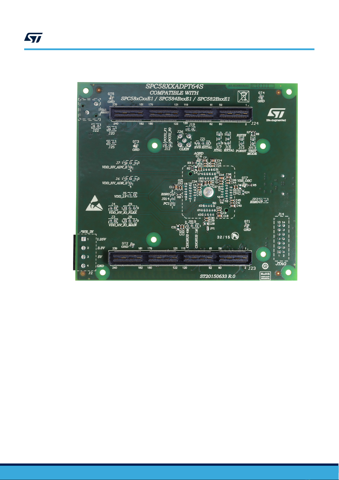
Table 1. Supply related jumpers
Jumper Description Default Position
J3 Jumper to enable the use of supply
3.3V_SR Closed Figure 4. SPC58XXADPT64S rev. B "mini module" -
top - D3
J4 Jumper to enable the use of supply
5.0V_SR Closed Figure 4. SPC58XXADPT64S rev. B "mini module" -
top - D3
J5 Jumper to enable the use of supply
1.25V_SR Closed Figure 4. SPC58XXADPT64S rev. B "mini module" -
top - A3
J6
VDD_HV_ADR_S voltage configuration,
select from 5.0V_LR (linear), 3.3V_SR
(switching) or 5.0V_SR (switching)
1-2 (5.0V_LR) Figure 4. SPC58XXADPT64S rev. B "mini module" -
top - D2
J7
VDD_HV_ADV_S voltage configuration,
select from 5.0V_LR (linear), 3.3V_SR
(switching) or 5.0V_SR (switching)
1-2 (5.0V_LR) Figure 4. SPC58XXADPT64S rev. B "mini module" -
top - D2
J8 VDD_HV_IO_MAIN voltage configuration,
select from 5.0V_SR or 3.3V_SR 1-2 (5.0V_SR) Figure 4. SPC58XXADPT64S rev. B "mini module" -
top - D3
J9
VDD_HV_IO_FLEX voltage configuration,
select from 5.0V_SR or 3.3V_SR (for
Chorus 4M with JR19 closed 2-3)
1-2 (5.0V_SR) Figure 4. SPC58XXADPT64S rev. B "mini module" -
top - D3
J16 VDD_LV voltage configuration, select from
1.25V_SR or from Ballast Circuit 1-2 (1.25V_SR) Figure 4. SPC58XXADPT64S rev. B "mini module" -
top - B3
J18 Ballast supply voltage configuration, select
from VDD_HV_IO_MAIN or from 5.0V_SR 1-2 (5.0V_SR) Figure 4. SPC58XXADPT64S rev. B "mini module" -
top - A3
JP1
VDD_HV_FLA voltage configuration,
connect or disconnect VDD_HV_FLA from
VDD_HV_IO_MAIN
Closed Figure 5. SPC58XXADPT64S rev. B "mini module" -
bottom - C3
UM2790
Power and system configuration
UM2790 - Rev 1 page 7/24

5.2 Microcontrollers configuration
The SPC58XXADPT64S rev. B "mini module" is designed to be easily configurable and be used for
SPC582BxxE1, SPC584BxxE1 and SPC58xCxxE1.
The "mini module" is configured by default for SPC582BxxE1 and easily supports SPC584BxxE1 and
SPC58xCxxE1 by simply changing the following through-hole jumper JR19.
Table 2. Microcontroller configuration related jumpers
Jumper Description Default Position
JR19
Device pin 62 port configuration / function
configuration:
• 1-2 - PC12 for SPC582BxxE1
• 2-3 - VDD_HV_IO_FLEX for
SPC584BxxE1 and SPC58xCxxE1
Closed 1-2
PC12 for
SPC582BxxE1
Figure 4. SPC58XXADPT64S rev. B "mini
module" - top - B3
5.3 Port configuration
The following jumpers need to configure the ports:
Table 3. Ports related jumpers
Jumper Description Default Position
JP13 TESTMODE settings Close (10 KΩ pull-
down)
Figure 4. SPC58XXADPT64S rev. B "mini
module" - top - A2
JR14
Device pin 6 port configuration / function
configuration:
• 1-2 (PC1)
• 2-3 (ESR0)
Open Figure 4. SPC58XXADPT64S rev. B "mini
module" - top - C3
J29
Device pin 56 port configuration /
function configuration:
• 1-2 (PH4) SPC582BxxE1
• 2-3 (BCTRL) SPC584BxxE1,
SPC58xCxxE
1-2 (PH4)
SPC582BxxE1
Figure 4. SPC58XXADPT64S rev. B "mini
module" - top - A3
5.4 Debug interface configuration
The following jumpers need to configure the ports:
Table 4. Debug interface configuration related jumpers
Jumper Description Default Position
J13
RSTIN connection
• open (disconnect PORST)
• closed (connect PORST)
Closed (connect
PORST)
Figure 4. SPC58XXADPT64S rev. B "mini module" -
top - B2
JP2
JTAG/LFAST LVDS pin 9 configuration
• open (disconnect ESR0)
• closed (connect ESR0)
Open (disconnect
ESR0)
Figure 4. SPC58XXADPT64S rev. B "mini module" -
top - A3
UM2790
Microcontrollers configuration
UM2790 - Rev 1 page 8/24

5.5 System clock configuration
The "mini module" supports the usage of the crystal clock sources as well as the external clock source:
Table 5. Clock configuration jumpers
Jumper Description Default Position
J15 40 MHz crystal clock source enable
for pin EXTAL 1-2 (XT1 pin2) Figure 4. SPC58XXADPT64S rev. B "mini module" - top -
B2
J17 40 MHz crystal clock source enable
for pin XTAL 1-2 (XT1 pin1) Figure 4. SPC58XXADPT64S rev. B "mini module" - top -
B2
J19 Enable 8 MHz oscillator power
supply Open Figure 4. SPC58XXADPT64S rev. B "mini module" - top -
B1
J21 External clock source from 8 MHz
oscillator or SMA connector
1-2
(8 MHz oscillator)
Figure 4. SPC58XXADPT64S rev. B "mini module" - top -
D1
UM2790
System clock configuration
UM2790 - Rev 1 page 9/24

5.6 Reset circuit
The "mini module" supports different ways to reset the microcontroller.
To use and perform the reset driving there are different jumpers and switches:
Table 6. Reset configuration jumpers
Jumper Description Default Position
SW1 Reset push button Open Figure 4. SPC58XXADPT64S rev. B "mini module" - top - D1
J22
Connect the external reset to the reset
driver for
ESR0 and PORST pins
Close Figure 4. SPC58XXADPT64S rev. B "mini module" - top - D1
J20 Connect the external reset to ESR0 pin Close Figure 4. SPC58XXADPT64S rev. B "mini module" - top - D1
J25 Connect the external reset to PORST pin Close Figure 4. SPC58XXADPT64S rev. B "mini module" - top - D2
5.7 Test points
The "mini module" has several test points. Below all test points description:
Table 7. Test points
Test point Description Position
GT1 GND test point Figure 4. SPC58XXADPT64S rev. B "mini module" - top - A2
GT2 GND test point Figure 4. SPC58XXADPT64S rev. B "mini module" - top - C4
GT3 GND test point Figure 4. SPC58XXADPT64S rev. B "mini module" - top - C2
GT4 GND test point Figure 4. SPC58XXADPT64S rev. B "mini module" - top - A1
GT5 GND test point Figure 4. SPC58XXADPT64S rev. B "mini module" - top - D1
GT6 AGND test point Figure 4. SPC58XXADPT64S rev. B "mini module" - top - B2
GT7 VSS_OSC test point Figure 4. SPC58XXADPT64S rev. B "mini module" - top - B3
TP1 TCK test point Figure 4. SPC58XXADPT64S rev. B "mini module" - top - A2
TP2 TMS/Txp test point Figure 4. SPC58XXADPT64S rev. B "mini module" - top - A3
TP3 TDI/Txn test point Figure 4. SPC58XXADPT64S rev. B "mini module" - top - A3
TP4 TDO/Rxp test point Figure 4. SPC58XXADPT64S rev. B "mini module" - top - A3
TP5 JCOMP/Rxn test point Figure 4. SPC58XXADPT64S rev. B "mini module" - top - A3
TP6 J23A, QSH connector, pin10 (PA5) test point Figure 4. SPC58XXADPT64S rev. B "mini module" - top - A4
TP7 J23A, QSH connector, pin11 (PA6) test point Figure 4. SPC58XXADPT64S rev. B "mini module" - top - A4
TP8 J23A, QSH connector, pin12 (PA7) test point Figure 4. SPC58XXADPT64S rev. B "mini module" - top - B4
TP9 J23A, QSH connector, pin13 (PA8) test point Figure 4. SPC58XXADPT64S rev. B "mini module" - top - B4
TP10 J23A, QSH connector, pin14 (PA9) test point Figure 4. SPC58XXADPT64S rev. B "mini module" - top - B4
5.8 Connectors
The "mini module" has the following connectors:
Table 8. Connectors
Connectors Description Position
J14 14-pin header connector for JTAG interface Figure 4. SPC58XXADPT64S rev. B "mini module" - top - A3
UM2790
Reset circuit
UM2790 - Rev 1 page 10/24

Connectors Description Position
CN1 10-pin header connector for JTAG/LFAST
LVDS interface Figure 4. SPC58XXADPT64S rev. B "mini module" - top - A2
J12 Fault collection and control unit (FCCU) pin,
for failure notification Figure 4. SPC58XXADPT64S rev. B "mini module" - top - C2
J23, J24 2 X Samtec QSH series, 240 way connector
to connect "mini module" to motherboard
Figure 5. SPC58XXADPT64S rev. B "mini module" - bottom -
A1/A4
J2 External power supplies input (5 V, 3.3 V,
1.25 V) Figure 4. SPC58XXADPT64S rev. B "mini module" - top - D4
J26 SMA connector for external clock input ) Figure 4. SPC58XXADPT64S rev. B "mini module" - top - C2
UM2790
Connectors
UM2790 - Rev 1 page 11/24

6Layout overview
Figure 4. SPC58XXADPT64S rev. B "mini module" - top
1
2
3
4
ABCD
UM2790
Layout overview
UM2790 - Rev 1 page 12/24

Figure 5. SPC58XXADPT64S rev. B "mini module" - bottom
1
2
3
4
ABCD
UM2790
Layout overview
UM2790 - Rev 1 page 13/24

7BOM
Table 9. BOM
Item QTY Reference Manufacturer Code Value Part description
1 7
C4, C10, C28,
C31, C47, C48,
C59
2.2 uF Mult. cer. cap. 16V 0805 - automotive
series - not mounted!
2 9
C5, C8, C11, C13,
C15, C17, C19,
C29, C32
CCERSMD104-0603M 100 nF Mult. cer. cap. 50V 0603
3 13
C6, C9, C22, C23,
C24, C25, C26,
C30, C33, C42,
C43, C44, C45
CCERSMD103-0603M 10 nF Mult. cer. cap. 50V 0603
4 7
C7, C34, C36,
C38, C40, C49,
C50
CCERSMD225-0805M 2.2 uF Mult. cer. cap. 16V 0805 - automotive
series
5 4 C12, C14, C16,
C18 CCERSMD475-0805M 4.7 uF Mult. cer. cap. 16V 0805
6 4 C35, C37, C39,
C41 CCERSMD473-0603M 47 nF Mult. cer. cap. 50V 0603
7 1 C51 47 pF DNP Mult. cer. cap. 50V SMD 0603 - not
mounted!
8 1 C52 CCERSMD270-0603 27 pF Mult. cer. cap. 50V SMD 0603
9 2 C53, C55 10 pF DNP Mult. cer. cap. 50V SMD 0603 - not
mounted!
10 2 C54, C57 DNM Mult. cer. cap. 50V SMD 0603 - not
mounted!
11 1 C56 CCERSMD104-0603M 100 nF Mult. cer. cap. 50V SMD 0603
12 1 C58 CCERSMD270-0603M 27 pF Mult. cer. cap. 50V SMD 0603
13 1 CN1 SAM-TFM10502LDWT Samtec TFM-105-02-
L-D-WT
Samtec 5x2 TFM connector - 1.27 mm
pitch - with weld Tabs
14 1 DUT1 ZOCC64ETQFP
CHORUS - device under test - TQFP64-
EP - SENSATA(WELLS) - 3010-064-
X-0G-ST
15 7
GT1, GT2, GT3,
GT4, GT5, GT6,
GT7
TEST2 TEST2 PCB test point - raised loops
16 1 J2 AST-0250404 AST0250404 Conn 4 pin, 90°, AST board mount
screwless
17 5 J3, J4, J5, J13,
JP13 STRIP2PM STRIP2PM Male strip 2 poles see mech part -
normally closed !!
18 2 J6, J7 STRIP3PM + STRIP1PM STRIP3PM +
STRIP1PM
Male strip 4 poles see mech part (close
pin 1 and 2)
19 10
J8, J9, J15, J16,
J17, J18, J21, J29,
JR14, JR19
STRIP3PM STRIP3PM Male strip 3 poles see mech part (close
pin 1 and 2)
20 1 J12 STRIP2PM STRIP2PM Male strip 2 poles
21 1 J14 M.14.180 LP-3M N2514-6002RB 3M conn flat male 14 pins, straight - pitch
2.54 mm
22 1 J19 STRIP2PM STRIP2PM Male strip 2 poles see mech part - open !
UM2790
BOM
UM2790 - Rev 1 page 14/24

Item QTY Reference Manufacturer Code Value Part description
23 3 J20, J22, J25 STRIP2PM STRIP2PM Male strip 2 poles see mech part - close !
24 2 J23, J24 SAM-QSH12001LDA Samtec QSH-120-01-
L-D-A
Samtec 0.5 mm pitch high speed SMD
socket
25 1 J26 BNC-SMA-FEM-180 BNC-SMA-FEM-180 Conn. RF SMA 180°
26 1 JP1 Jumper SMD - close! - with a solder
drop !
27 1 JP2 STRIP2PM STRIP2PM Male strip 2 poles see mech part -
normally open !
28 1 LD1 LEDSMDGIAL-0805 Yellow Led Diode Yellow SMD 0805
29 1 LD2 LEDSMDRED-0805 Red Led diode red SMD 0805
30 1 OSC1 Q8MHZ-SMD-3953M 8 MHz Hybrid quartz osc SMD ECS 3953M
31 1 Q2 TRNJD2873-SMD NJD2873 NPN plastic Power transistor DPAK
32 1 R2 RESMD000-805-5 0R Resistor 1/10W 5% 0805
33 6 R3, R5, R27, R28,
R29, R30 RESMD000-0603 0R Resistor 1/10W 1% 0603
34 2 R6, R9 RESMD472-0603 4K7 Resistor 1/10W 1% 0603
35 2 R7, R11 10K DNP Resistor 1/10W 1% SMD 0603 - not
mounted!
36 1 R8 RESMD103-0603 10K Resistor 1/10W 1% 0603
37 1 R10 RESMD0R1-1206 0R1 Resistor 1/2W 1% 1206
38 2 R12, R18 RESMD103-0603 10K Resistor 1/10W 1% SMD 0603
39 1 R13 RESMD000-0603 0R Resistor 1/10W 1% SMD 0603
40 2 R16, R17 RESMD561-0603 560R Resistor 1/10W 1% SMD 0603
41 2 R19, R21 RESMD221-0603 220R Resistor 1/10W 1% SMD 0603
42 1 R20 RESMD472-0603 4K7 Resistor 1/10W 1% SMD 0603
43 1 R22 RESMD49R9-0603 49R9 Resistor 1/16W 1% 0603
44 1 R24 100R Resistor 1/10W 1% 0603 - not mounted!
45 2 R25, R26 DNM Resistor 1/16W 1% SMD 0603 - not
mounted!
46 1 SW1 PULSANTECS Pushbutton Pushbutton NO low profile for pcb
47 10
TP1, TP2, TP3,
TP4, TP5, TP6,
TP7, TP8, TP9,
TP10
TESTPOINT Test point SMD - not mounted!
48 1 U1 74LVC125AMTR-SMD 74LVC125AMTR I.C. quad bus buffers SO14
49 1 U2 74V1G08-SMD 74V1G08STR I.C. single 2-input and gate - SMD
SOT23-5L
50 1 XT1 Q40MHZ-SMD-5032 40 MHz Quartz 40 MHz SMD NX5032GA XTAL
NDK
UM2790
BOM
UM2790 - Rev 1 page 15/24

8Schematics
Figure 6. Power and decoupling
J3
de fault CLOSED
J4
de fault CLOSED
J5
defau lt CLOSED
0603
100nF
50V
X7R
C5
VDD_HV_ADR_S
0603
10nF
50V
X7R
C6
AGND AGND
0603
100nF
50V
X7R
C8
VDD_HV_ADV_S
0603
10nF
50V
X7R
C9
AGND AGND
1-2 CLOSED
DEFAULT
2
13
J8
0603
100nF
50V
X7R
C29
0603
10nF
50V
X7R
C30
GND GND
0805
2.2uF
16V
X7R
C28
GND
N.M.
default CLOSE
JP1
0805
2.2uF
16V
X7R
C36
0603
47nF
50V
X7R
C37
0603
10nF
50V
X7R
C43
GND GND GND
0805
2.2uF
16V
X7R
C38
0603
47nF
50V
X7R
C39
0603
10nF
50V
X7R
C44
Pin 33
GND GND GND
0805
2.2uF
16V
X7R
C40
0603
47nF
50V
X7R
C41
0603
10nF
50V
X7R
C45
GND GND GND
Pin 27
0805
2.2uF
16V
X7R
C34
0603
47nF
50V
X7R
C35
0603
10nF
50V
X7R
C42
Pin 11
GND GND GND
Pin 47
VDD_LV
1-2 CLOSED
DEFAULT
2
1 3
J9
0603
100nF
50V
X7R
C32
0603
10nF
50V
X7R
C33
GND GND
VDD_HV_IO_F LEX
VDD_LV
AGND
N.M.
0805
2.2uF
16V
X7R
C4
0805
2.2uF
16V
X7R
C7
AGND
5.0V_SR3.3V_SR 1.25V_SR5.0V_LR
1-2 CLOSED
DEFAULT
1-2 CLOSED
DEFAULT
5.0V_SR
5.0V_SR
2
1
3
4
J7
2
1
3
4
J6
0805
2.2uF
16V
X7R
C31
GND
N.M.
Pin 57
0805
4.7uF
16V
X7R
C12
GND
0603
100nF
50V
X7R
C13
0603
10nF
50V
X7R
C23
GND GND
Pin 12
0805
4.7uF
16V
X7R
C14
GND
0603
100nF
50V
X7R
C15
0603
10nF
50V
X7R
C24
GND GND
Pin 28
0805
4.7uF
16V
X7R
C16
GND
0603
100nF
50V
X7R
C17
0603
10nF
50V
X7R
C25
GND GND
Pin 34
0603
100nF
50V
X7R
C11
0603
10nF
50V
X7R
C22
VSS_OSC VSS_OSCVSS_OSC
N.M.
0805
2.2uF
16V
X7R
C10
Pin 38
0805
4.7uF
16V
X7R
C18
GND
0603
100nF
50V
X7R
C19
0603
10nF
50V
X7R
C26
GND GND
Pin 49
VDD_HV_IO_MA IN
VDD_HV_IO_MAIN
0R
1/10W
0805
R2
5.0V_SR3.3V_SR1.25V_SR
GND
GND
GT1
TE ST2
GT2
TE ST2
GT3
TE ST2
GT4
TE ST2
GT5
TE ST2
RING -HE ADED FOR PROBE HOOK
AGND
GT6
TE ST2
0R
1/10W
0603
R5
VSS_OSC GND
0R
1/10W
0603
R3
AGND GND
VSS_OSC
GT7
TE ST2
AGND
VSS_OSC
GND
VDD_HV_IO_FLEX
1-2 CLOSED
DEFAULT
2
13
J16
NJD2873
Q2
Thermal plane
0805
2.2uF
16V
X7R
C49
0805
2.2uF
16V
X7R
C50
0805
2.2uF
16V
X7R
C59
N.M.
0805
2.2uF
16V
X7R
C47
N.M.
0805
2.2uF
16V
X7R
C48
N.M.
GND
GND
for power 2W/3W
1-2 CLOSED
GNDGND
0R1
1/2W
1206
R10
2
1
3
J18
VDD_HV_IO_M AIN
5.0V_SR
DEFAULT
BCTRL
BCTRL
1
2
3
4
AST 0250404
J2
VDD_HV_ADV_S 22
VDD_HV_JT AG_OSC 38
VDD_HV_IO_W0 12
VDD_HV_IO0_S0 28
VDD_HV_IO0_E0 34
VDD_HV_ADR_S 20
ADC
OSC & JTAG (3.3V or 5V)
I/O (3.3v - 5V)
VSS_HV_ADR_S
19
VSS_HV_ADV_S
21
VSS_HV_OSC
35
MCU CORE LOGIC (1.25V)
Power Pins
VDD_HV_FLA 57
VDD_LV_W3 11
EPAD
65
VDD_LV_S0 27
VDD_L V_E5 33
VDD_LV_E3 47
FLASH DECOUPLING
Power Bar
DUT1A
VDD_HV_IO0_N0 49
SPC58xCxxE1 /
SPC584BxxE1 /
SPC582BxxE1
UM2790 - Rev 1 page 16/24
UM2790
Schematics

Figure 7. Signals
4K 7
1/10W
060 3
R9
VDD_HV_IO_M AIN
ESR0 E SR0 PC1
PI[0..15 ]
PI[0..15 ]
PI1
PI2
PI3
PI4
PI6
PI7
PH[0..15 ]
PH[0..15 ]
PG[0..15 ]
PG[0..15 ]
PG10
PG11
PG12
PF[0..15 ]
PF [0..15 ]
PF2
PF3
PE[0..15 ]
PE [0..15 ]
PE 2
PE 3
PE 10
PE11
EXTA L
XTA L
PORS T
JP 13
default CL OSE D
10K DNP
1/10W
0603
R7
10K
1/10W
0603
R8
GND
VDD_HV_IO_M AIN
NOT MOUNTED
PD[0..15]
PD[0..15]
PD0
PD5
PD11
PD12
PD13
PD14
PD15
PC[0..15]
PC[0..15 ]
PC1
PC2
PC3
PC4
ST RIP 2P M
J12
FCC U_F1 LABEL ON PCB
FCC U_F0 LABEL ON PCB
JCOMP/Rxn
TDO/Rxp
TDI T/ xn
TMS T/ xp
TCK
TP5TP4TP3TP2TP1
RST IN
PORST
PC13
PC14
PC15
4K7
1/10W
0603
R6
VDD_HV_IO_M AIN
PB[0..15]
PB [0..15 ]
PB 8
PB 9
PB 10
PB 1 1
2
13
JR14
1-2 CLOSE D
DEFAUL T
PA[1 ]
51
PA[2 ]
50
TCK / PA[6]
43
TMS / PA[7 ]
40
TDI / PA[8 ]
39
TDO / PA[9]
41
PA[10 ]
52
PA[11 ]
53
PB[8 ]
32
PB[9 ]
31
PB[10 ]
30
PB[11] / FCCU_F0
29
PD[0 ]
58
PD[5 ]
48
PD[11 ]
26
PD[12 ]
8
PD[13 ]
9
PF[2 ] 64
PF[3 ] 63
PG[10] 23
PG[11] 24
PG[12] 25
PE[2 ] 7
PE[3 ] 10
PE[10 ] 54
PE[11 ] 55
PORS T
45
TE ST MODE
44
XTA L
37
EXTA L
36
SPC58xCxxE1 / SPC584BxxE1 / SPC582BxxE1 Port Pins
PC[13 ]
61
PC[14 ]
60
PC[15 ]
59
PC[2] / FCCU_F1
5
PC[3]
4
PC[4]
3
PD[14 ]
1
PD[15 ]
2
PH[4 ] 56
PC[1 ] 6
JCOMP / PA[5 ]
42
PI[7 ] 18
PI[6 ] 17
PI[4 ] 16
PI[3 ] 15
PI[2 ] 14
PI[1 ] 13
PC[12]/VDD_HV_IO_FLEX
62
PM[14 ] 46
DUT1B
PA[0..15]
PA [0..15 ]
PA1
PA2
PA 10
PA11
default CLOSED
J13
1-2 CLOSE D
DEFAUL T
2
1 3
JR19
PC12 VDD_HV_IO_FLEX
PIN62
Jumper setting
2-3 : Chorus 4M
1-2 : Chorus 1M
PM14
BCTRL
1-2 CLOSE DDEFAULT
2
13
J29
BCTRL PH4
UM2790 - Rev 1 page 17/24
UM2790
Schematics

Figure 8. JTAG, JTAG/LFast LVDS INTERFACE, reset and crystal
EXTAL
XTAL
EVB-EXTAL
ESR0
RSTIN
RST-MCU
OSC-MOD
EVB-EXTAL
EXTAL-SMA
RST-SW
VCC
GND
2 3
14
1
7
74LVC125AMTR
U1A
I2
5O2 6
OE2 4
74LVC125AMTR
U1B
VDD_HV_IO_MAIN
VDD_HV_IO_MAIN
VDD_HV_IO_MAIN
VDD_HV_IO_MAIN
3.3V_SR
VDD_HV_IO_MAIN
XTAL
EXTAL
ESR0
RSTIN
RST-SW
GND
GND
GND
GND
GND
GND
GND
GND
(MCU Crystal Input)
(MCU Crystal Output)
1-2 CLOSED
DEFA ULT
1-2 CLOSED
DEFA ULT
default OPEN
1-2 CLOSED
DEFA ULT
GND
default CLOSED
default CLOSED
default CLOSED
REMOVE XTAL jumper when driving EXTAL from
Oscillator Module or External Source (PLL Enabled)
Connect XTAL jumper to GND when driving EXTAL from
Oscillator Module or External Source (PLL Bypass Mode)
Note - External 3.3V
regulator MUST be
enabled when using
oscillator module
Note - Internal
Pull-Up on Pin 1
SMA style
Connector
USER RESET LED
External Clock Input
MCU RESET LED
RESET
SO14
I3
9O3 8
OE 310
74LVC125AMTR
U1C
SO14
SO14
NOT MOUNTED
NOT MOUNTED
2
13
STRIP3PM
J17
0R
1/10W
0603
R13
1 2
40MHz
NX5032GA
XT1
0603
10pF DNP
50V
COG/NP0
C53
0603
10pF DNP
50V
COG/NP0
C55
0603
100nF
50V
X7R
C56
STRIP2PM
J19
2
13
STRIP3PM
J21
49R9
1/16W
0603
1%
R22
EN
1
GND
2OUT 3
+Vs 4
8MHz
7x5
OSC1 10K
1/10W
0603
R18
560R
1/10W
0603
R16
4K7
1/10W
0603
R20
STRIP2PM
J22
Yellow
0805
LD1 STRIP2PM
J20
STRIP2PM
J25
220R
1/10W
0603
R19
220R
1/10W
0603
R21
560R
1/10W
0603
R17
Red
0805
LD2
2
1 3
STRIP3PM
J15
1
2
BNC-SMA-FEM-180
J26
ENABL E
GND
VCC
1
2
4
53
74V1G08STR
SOT23-5L
U2
RSTIN
TDI
TDO
TCK
JCOMP
TMS
GND GND
GND
NOT MOUNTED
Jtag interface
TDI, TDO, TCK, TMS & JCOMP are not connected to daughter card.
PORST, ESR0, are connected to daughtercard
JTAG Connector
NOT MOUNTED
GND
1 2
3 4
5 6
7 8
9 10
11 12
13 14
N2514-6002RB
J14
10K
1/10W
0603
R12
10K DNP
1/10W
0603
R11
0603
27pF
50V
COG/NP0
C52
0603
47pF DNP
50V
COG/NP0
C51
Pushbutton
SW1
VDD_HV_IO_MAIN
VDD_HV_IO_MAIN
VSS_OSC
JCOMP/Rxn
TCK
TDI/Txn
TDO/Rxp
TMS/Txp
GND GND
GND
GND
DNM
1/16W
0603
R26
DNM
1/16W
0603
R25
0603
DNM
X7R
C54
0603
DNM
X7R
C57
0603
27pF
50V
COG/NP0
C58
JTAG/LFast LVDS INTERFACE
10 Pin Version
NOT MOUNTED !!!
VDD_HV_IO_MAIN
VDD_HV_IO_MAIN
RSTIN
d iff ere nti a l s ig n a ls
0R
1/10W
0603
R30
0R
1/10W
0603
R29
0R
1/10W
0603
R28
0R
1/10W
0603
R27
JCOMP TMS TDI TDO
100R
1/10W 0603
R24
default OPEN
JP2
ESR0
1 2
3 4
5 6
7 8
9 10
GND
12 GND 11
SAMTEC TFM-105-02-L-D-WT
CN1
GND
GND
UM2790 - Rev 1 page 18/24
UM2790
Schematics

Figure 9. Motherboard connectors
PA8
PG10
PG12
5.0V_SR
PE2
PE10
1.25V_SR
PC2
PC4
5.0V_SR
PC14
3.3V_SR
1.25V_SR
PA2
PA10
5.0V_SR
1.25V_SR
3.3V_SR
1.25V_SR
5.0V_SR
PA9
PG11
5.0V_SR
PE11
1.25V_SR
PE3
PC1
PC3
PC13
PC15
3.3V_SR
1.25V_SR
PA1
PA11
5.0V_SR
5.0V_SR
1.25V_SR
3.3V_SR
5.0V_SR
1.25V_SR
VDD_ HV_ IO_MA IN
5.0V_LR
5.0V_LR
3.3V_SR
3.3V_SR
5.0V_SR
5.0V_SR
1.25V_SR
1.25V_SR
VDD_ HV_ IO_MA IN
VDD_ HV_ IO_MA IN
5.0V_LR
5.0V_LR
VDD_ HV_ IO_MA IN
3.3V_SR
3.3V_SR
5.0V_SR
5.0V_SR
1.25V_SR
1.25V_SR
PF2
PG10
PG11
PG12
PH4
PC1
PC13
PC14
PC15
PA1
PA2
PA10
PA11
PB8
PB9
PB10
PB11
PD0
PD5
PD11
PD12
PD13
PD14
PD15
PE2
PE3
PE10
PE11
1.25V_SR
5.0V_LR
3.3V_SR
5.0V_SR
VDD_ HV_ IO_MA IN
1.25V_SR
5.0V_SR
3.3V_SR
1.25V_SR
3.3V_SR
1.25V_SR
1.25V_SR
3.3V_SR
PF3
5.0V_SR
PD5
PD11
PD13
PD15
3.3V_SR
PB9
PB11
3.3V_SR
PH4
1.25V_SR
3.3V_SR
PF2
5.0V_SR
PD0
PD12
PD14
1.25V_SR
PB8
PB10
1.25V_SR
5.0V_SR
3.3V_SR
1.25V_SR
3.3V_SR
5.0V_LR
1.25V_SR
1.25V_SR
5.0V_SR
5.0V_SR
3.3V_SR
3.3V_SR
VDD_ HV_ IO_MA IN
5.0V_LR
VDD_ HV_ IO_MA IN
5.0V_LR
1.25V_SR
1.25V_SR
5.0V_SR
5.0V_SR
3.3V_SR
3.3V_SR
VDD_ HV_ IO_MA IN
5.0V_LR
VDD_ HV_ IO_MA IN
RS T-SW
3.3V_SR1.25V_SR 5.0V_LR5.0V_SR VDD_HV_IO_M AIN
RST -SW
PortE
GND
GND
GND
TP6
PA[0..15] PB[0..15] PC[0..15] PD[0..15] PE[0..15] PF[0..15] PG[0..15] PH[0..15]
PortA PortB PortC PortD PortF PortG PortH
1
1
3
3
5
5
7
7
9
9
11
11
13
13
15
15
17
17
19
19
21
21
23
23
25
25
27
27
29
29
31
31
33
33
35
35
37
37
39
39
41
41
43
43
45
45
47
47
49
49
51
51
53
53
55
55
57
57
59
59
61
61
63
63
65
65
67
67
69
69
71
71
73
73
75
75
77
77
79
79
81
81
83
83
85
85
87
87
89
89
91
91
93
93
95
95
97
97
99
99
101
101
103
103
105
105
107
107
109
109
111
111
113
113
115
115
117
117
119
119
22
44
66
88
10 10
12 12
14 14
16 16
18 18
20 20
22 22
24 24
26 26
28 28
30 30
32 32
34 34
36 36
38 38
40 40
42 42
44 44
46 46
48 48
50 50
52 52
54 54
56 56
58 58
60 60
62 62
64 64
66 66
68 68
70 70
72 72
74 74
76 76
78 78
80 80
82 82
84 84
86 86
88 88
90 90
92 92
94 94
96 96
98 98
100 100
102 102
104 104
106 106
108 108
110 110
112 112
114 114
116 116
118 118
120 120
SA MTE C QSH-120-01-L-D-A
J23A
SH1
SH1
SH2
SH2
SH3
SH3
SH4
SH4
SH5
SH5
SH6
SH6
SH7
SH7
SH8
SH8
SH9 SH9
121
121
123
123
125
125
127
127
129
129
131
131
133
133
135
135
137
137
139
139
141
141
143
143
145
145
147
147
149
149
151
151
153
153
155
155
157
157
159
159
161
161
163
163
165
165
167
167
169
169
171
171
173
173
175
175
177
177
179
179
181
181
183
183
185
185
187
187
189
189
191
191
193
193
195
195
197
197
199
199
201
201
203
203
205
205
207
207
209
209
211
211
213
213
215
215
217
217
219
219
221
221
223
223
225
225
227
227
229
229
231
231
233
233
235
235
237
237
239
239
SH16 SH16
SH15 SH15
SH14 SH14
SH13 SH13
SH12 SH12
SH11 SH11
SH10 SH10
122 122
124 124
126 126
128 128
130 130
132 132
134 134
136 136
138 138
140 140
142 142
144 144
146 146
148 148
150 150
152 152
154 154
156 156
158 158
160 160
162 162
164 164
166 166
168 168
170 170
172 172
174 174
176 176
178 178
180 180
182 182
184 184
186 186
188 188
190 190
192 192
194 194
196 196
198 198
200 200
202 202
204 204
206 206
208 208
210 210
212 212
214 214
216 216
218 218
220 220
222 222
224 224
226 226
228 228
230 230
232 232
234 234
236 236
238 238
240 240
SA MTE C QSH-120-01-L-D-A
J23B
11
33
55
77
99
11 11
13 13
15 15
17 17
19 19
21 21
23 23
25 25
27 27
29 29
31 31
33 33
35 35
37 37
39 39
41 41
43 43
45 45
47 47
49 49
51 51
53 53
55 55
57 57
59 59
61 61
63 63
65 65
67 67
69 69
71 71
73 73
75 75
77 77
79 79
81 81
83 83
85 85
87 87
89 89
91 91
93 93
95 95
97 97
99 99
101 101
103 103
105 105
107 107
109 109
111 111
113 113
115 115
117 117
119 119
2
24
46
68
810
10 12
12 14
14 16
16 18
18 20
20 22
22 24
24 26
26 28
28 30
30 32
32 34
34 36
36 38
38 40
40 42
42 44
44 46
46 48
48 50
50 52
52 54
54 56
56 58
58 60
60 62
62 64
64 66
66 68
68 70
70 72
72 74
74 76
76 78
78 80
80 82
82 84
84 86
86 88
88 90
90 92
92 94
94 96
96 98
98 100
100 102
102 104
104 106
106 108
108 110
110 112
112 114
114 116
116 118
118 120
120
SA MTE C QSH-120-01-L-D-A
J24A
SH1 SH1
SH2 SH2
SH3 SH3
SH4 SH4
SH5 SH5
SH6 SH6
SH7 SH7
SH8 SH8
SH9
SH9
121 121
123 123
125 125
127 127
129 129
131 131
133 133
135 135
137 137
139 139
141 141
143 143
145 145
147 147
149 149
151 151
153 153
155 155
157 157
159 159
161 161
163 163
165 165
167 167
169 169
171 171
173 173
175 175
177 177
179 179
181 181
183 183
185 185
187 187
189 189
191 191
193 193
195 195
197 197
199 199
201 201
203 203
205 205
207 207
209 209
211 211
213 213
215 215
217 217
219 219
221 221
223 223
225 225
227 227
229 229
231 231
233 233
235 235
237 237
239 239
SH16
SH16
SH15
SH15
SH14
SH14
SH13
SH13
SH12
SH12
SH11
SH11
SH10
SH10
122
122 124
124 126
126 128
128 130
130 132
132 134
134 136
136 138
138 140
140 142
142 144
144 146
146 148
148 150
150 152
152 154
154 156
156 158
158 160
160 162
162 164
164 166
166 168
168 170
170 172
172 174
174 176
176 178
178 180
180 182
182 184
184 186
186 188
188 190
190 192
192 194
194 196
196 198
198 200
200 202
202 204
204 206
206 208
208 210
210 212
212 214
214 216
216 218
218 220
220 222
222 224
224 226
226 228
228 230
230 232
232 234
234 236
236 238
238 240
240
SA MTE C QSH-120-01-L-D-A
J24B
PA5
PA7PA6
VDD_ HV_ IO_FLEX
VDD_ HV_ IO_FLEXVDD_ HV_ IO_FLEX
PI3
VDD_ HV_ IO_FLEX
VDD_HV_IO_FLEX
TP7 TP8
TP10TP9
PC2
PC3
PC4
PF3
PI[0..15]
PI[0..15]
PortI
PI1
PI2
PI3
PI4
PI6
PI7
PI1
PI2
PI4
PI7PI6
PC12
PC12
PM14
UM2790 - Rev 1 page 19/24
UM2790
Schematics

Revision history
Table 10. Document revision history
Date Version Changes
17-Feb-2021 1 Initial release.
UM2790
UM2790 - Rev 1 page 20/24
Table of contents
Other ST Motherboard manuals

ST
ST STEVAL-IPE005V1 User manual

ST
ST STM32H7 Nucleo-144 User manual

ST
ST EVAL-L99MOD5xXP User manual

ST
ST STEVAL-PCC010V1 User manual

ST
ST FDA803S User manual

ST
ST STM3210E-EVAL User manual

ST
ST ST7 Series User manual

ST
ST STEVAL-ISC004V1 User manual

ST
ST STM3220G-EVAL User manual

ST
ST STM32H7B3I-EVAL User manual

ST
ST STEVAL-IHM022V1 User manual

ST
ST STM32746G-EVAL User manual

ST
ST EVALCOMMBOARD User manual

ST
ST STM32L5 Nucleo-144 board User manual

ST
ST SGS-Thomson ST624x-KIT Series User manual

ST
ST SPC584BADPT176S User manual

ST
ST STEVAL-IFS012V1 User manual

ST
ST STEVAL-AKI002V1 User manual

ST
ST EVAL-L99H02QF User manual

ST
ST STM32 Nucleo-64 User manual