DocID10240 Rev 2 3/17
AN1897 Application description and design
17
1 Application description and
design
1.1 Schematics
The overall schematic is shown in Figure 3.
1.1.1 Start-up phase
The VIPer22A-E has an integrated high voltage current source linked to the drain pin. At the
start-up converter, it charges the V
DD
capacitor until it reaches the start-up level (14.5 V),
and the VIPer22A-E starts switching.
1.1.2 Auxiliary
supply
The VIPer22A-E has a wide operating voltage range from 8 V to 42 V, respectively minimum
and maximum values for undervoltage and overvoltage protections.
This function is very useful to achieve low standby total power consumption. The feedback
loop is connected to 5 V output by D12 to regulate 5 V output. +5 V
stb
output is blocked by
Q3, so +5 V
stb
regulation is neglected. When the standby signal is present, the Q3 V
ce
cannot provide enough voltage to maintain D12 conducted, so the 5 V output is blocked,
and the +5 V
stb
output is connected to the feedback loop. In this condition the +5 V
stb
is
regulated. Thanks to the transformer structure, all the other secondary outputs and the
auxiliary voltages are pulled down to a very low level, also pulling down the total power
consumption. These features are below-indicated.
– In normal full load, the VDD voltage must be lower than the overvoltage protection.
– In short-circuit, the VDD voltage must be lower than the shutdown voltage.
Actually, this condition leads to the well-known hiccup mode.
– In no-load condition, the VDD voltage must be higher than the shutdown voltage.
1.1.3 Burst mode
The Viper22A-E integrates a current mode PWM with a power MOSFET and includes the
leading edge blanking function. The burst mode allows the VIPer22A-E to skip some
switching cycles when the energy drained by the output load goes below E = (T
b
*V
in
)2 *
f
sw
/2L
p
(T
b
= blanking time, V
in
= DC input voltage, f
sw
= switching frequency, Lp = primary
Inductance). The consequence is the reduction of the switching losses in case of low load
condition by reducing the switching frequency.
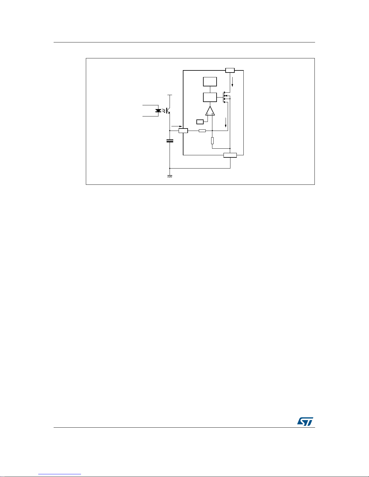
1.1.4 Feedback loop
The 5 V output voltage is regulated by a TL-431 (U3) via an optocoupler (U2) to the
feedback pin. If the output voltage is high, the TL-431 draws more current through its
cathode to the anode and the current increases in the optocoupler diode. The current in
optocoupler NPN increases accordingly and the current into the VIPer22A-E FB pin
increases. When the FB current increases, the VIPer22A-E skips some cycles to decrease
turn-on time and lower the output voltage to the proper level (see Figure 1). The 5 V output
voltage is regulated thanks to the TL-431 reference voltage and the R8 and R9 resistive
dividers.