ST PowerSTEP01 EVLPOWERSTEP01 User manual

Introduction
The EVLPOWERSTEP01 evaluation board is based on the powerSTEP01 system-in-package implementing a complete stepper
motor driver for high power applications. It is designed to operate with a supply voltage ranging from 10.5 V to 85 V with a
maximum current of 10 Arms.
In combination with the STEVAL-PCC009V2 evaluation board and the SPINFamily evaluation tool, the board provides a
complete and easy to use evaluation environment allowing the user to investigate all the features of powerSTEP01.
With daisy chain configuration support, the board is suitable for evaluation of multimotor applications.
Figure 1. EVLPOWERSTEP01 evaluation board
PowerSTEP01 system-in-package integrating microstepping controller and 10 A
power MOSFETs evaluation board
UM1829
User manual
UM1829 - Rev 2 - March 2022
For further information contact your local STMicroelectronics sales office.
www.st.com

1Board description
Table 1. EVLPOWERSTEP01 electrical specifications
Parameter Value
Supply voltage (VS) 10.5 V to 85 V
Maximum output current (each phase) 10 Arms
Gate drivers supply voltage (VCC) 7.5 V to 15 V
Logic supply voltage 3.3 V
Logic interface supply voltage 3.3 V or 5 V
Low logic level input 0 V
High logic level input VDD(1)
Operating ambient temperature 0 °C to +85 °C
1. All logic inputs are 5 V tolerant.
Figure 2. EVLPOWERSTEP01 jumper and connector locations
Master
SPI connector
FLAG LED
BUSY LED
Slave
SPI connector
Power supply connector
(10.5 V - 85 V)
Motor supply voltage
compensation trimmer
(ADCIN input)
STCK
input
VS
test point
VREG
test point
STBY pull-up
jumper
VDD
test point
VCC test point
Ground test point
Ground test point
External oscillator
connector
(OSCIN and OSCOUT)
External switch
connector
(SW input)
SPI termination
jumper
Supply management connector
(VS, VSREG, VCCREG
and GND)
Supply management
jumpers
Motor phase B
connector
Bridge B
shunt resistors
Bridge A
shunt resistors
Motor phase A
connector
powerSTEP01
Table 2. Jumpers and connectors description
Name Type Function
J4 Power supply Main supply voltage
J1 Power output Power bridge A outputs
J3 Power output Power bridge B outputs
J6 Power supply Integrated voltage regulator inputs
J5 SPI Master SPI connector
J7 SPI Slave SPI connector
JP3 Jumper VS to VSREG jumper
JP4 Jumper VSREG to VCC jumper
UM1829
Board description
UM1829 - Rev 2 page 2/21

Name Type Function
JP5 Jumper VCC to VCCREG jumper
JP6 Jumper VCCREG to VREG jumper
JP7 Jumper VREG to VDD jumper
JP8 Jumper VDD to 3.3 V from SPI connector jumper
JP9 Jumper Daisy chain termination jumper
JP10 Jumper STBY to VS pull-up jumper
Table 3. Master SPI connector pinout (J5)
Pin number Type Function
1 Open drain output powerSTEP01 BUSY output
2 Open drain output powerSTEP01 FLAG output
3 Ground Ground
4 Supply EXT_VDD (can be used as external logic power supply)
5 Digital output SPI “Master In Slave Out” signal (connected to powerSTEP01 SDO output through daisy
chain termination jumper JP9)
6 Digital input SPI “Serial Clock” signal (connected to powerSTEP01 CK input)
7 Digital input SPI “Master Out Slave In” signal (connected to powerSTEP01 SDI input)
8 Digital input SPI “Slave Select” signal (connected to powerSTEP01 CS input)
9 Digital input powerSTEP01 step-clock input
10 Digital input powerSTEP01 standby/reset input
Table 4. Slave SPI connector pinout (J7)
Pin number Type Function
1 Open drain output powerSTEP01 BUSY output
2 Open drain output powerSTEP01 FLAG output
3 Ground Ground
4 Supply EXT_VDD (can be used as external logic power supply)
5 Digital output SPI “Master In Slave Out” signal (connected to pin 5 of J5)
6 Digital input SPI “Serial Clock” signal (connected to powerSTEP01 CK input)
7 Digital input SPI “Master Out Slave In” signal (connected to powerSTEP01 SDO output)
8 Digital input SPI “Slave Select” signal (connected to powerSTEP01 CS input)
9 Digital input powerSTEP01 step-clock input
10 Digital input powerSTEP01 standby/reset input
UM1829
Board description
UM1829 - Rev 2 page 3/21

1.1 EVLPOWERSTEP01 schematics
Figure 3. EVLPOWERSTEP01 schematic 1 of 2
Application reference
OUTA1
OUTA2
OUTB1
OUTB2
STBY_RESET
nCS
CK
SDI
BUSY
FLAG
STCK
SW
SDO
ADC_IN
VS
VS_REG
VCC
VCC_REG
VREG
VDD
VDD VDD
C12
100 nF/4 V
R8
J1
1
2
C9 100 nF/25 V
D1BAR43SFILM
12
3
C8
470 nF/25 V
JP1
OPEN
C7100 nF/100 V
C2
220 nF/100 V
R5
R2
C1
470 nF/25 V
R1
J2
N.M.
1
2
JP2
OPEN
C6
47 nF/100 V
U1
powerSTEP01
OUTB2 7
OUTB2 81
OUTB2 85
OUTB2 97
OUTB1 65
OUTB1 80
OUTB1 76
OUTB1 96
OUTA2 22
OUTA2 33
OUTA2 37
OUTA2 92
OUTA1 38
OUTA1 53
OUTA1 42
OUTA1 93
SENSEA_P
34
SENSEA_P
35
SENSEA_P
36
SENSEB_P
78
SENSEB_P
82
SENSEB_P
79
CP
57
VS
55
VBOOT
56
VSREG
61
VCC
58
VCCREG
60
VREG
62
VS
1
VS
2
VS
3
VS
4
VS
5
VS
6
VS
23
VS
24
VS
25
VS
26
VS
27
VS
28
VS
29
VS
30
VS
31
VS
32
VS
43
VS
44 VS
45
VS
46
VS
47
VS
48
VS
49
VS
50
VS
66
VS
67
VS
68
VS
69
VS
70
VS
71
VS
72
VS
73
VS 86
VS 87
VS 90
SENSEA_P
39
SENSEB_P 83
GND
8
GND 21
GND
59
SENSEA_S 20
SENSEB_S 9
STCK
17
CK
11
SDI
12
VDDIO
13
SDO
14
BUSY_SYNC
15
FLAG
16
SW
18
STBY_RESET
19
CS
10
OSCIN
63
OSCOUT
64
ADCIN 54
SENSEA_P 40
SENSEB_P
77
SENSEB_P
84
GND
98
VS
51
VS
52
VS
74
VS 75
VS 88
VS 89
VS 91
VS 94
VS 95
SENSEA_P
41
SENSEA_P
99
SENSEA_P
100
SENSEB_P
101
SENSEB_P
102
R4
C13
100 nF/6.3 V
C5
220 nF/100 V
C10 3.3 nF/6.3 V
C4
220 nF/100 V
C3
220 nF/100 V
R3
0R1/2W
C11
/6.3 V
R7
J3
1
2
UM1829 - Rev 2 page 4/21
UM1829
EVLPOWERSTEP01 schematics

Figure 4. EVLPOWERSTEP01 schematic 2 of 2
SPI_IN
SPI_OUT
VS
VS_REG
VCC_REG
GND
OPTION
VS
GND
10.5 V - 85 V
SDO
STBY_RESET
STBY_RESET
STCK
STCK
nCS
CK
SDI
BUSY
BUSY
FLAG
FLAG
nCS
CK
FLAG
BUSY
STCK
STBY_RESET ADC_IN
nCS
CK
SDI
SDO
FLAG
BUSY
STBY_RESETSTCK
SW
3V3
3V3
VDD VDD
3V3
VS VS_REG VCC VCC_REG VREG VDD
VDDVS_REG VS
VS_REG VCC_REGVS
VS
R14
R15
13
2
J8
N.M.
1
2
D2
BZX585-B3V3
R11
C15
10 nF/6.3 V
J7
1 2
3 4
5 6
7 8
9 10
JP9
12
JP4
1 2
J5
1 2
3 4
5 6
7 8
9 10
TP2
1
VDD
1
JP10
1 2
DL2
LED - RED
2 1
VREG
1
DL1
LED - AMBER
21
J6
N.M.
1
2
3
4
STCK 1
VCC
1
VS
1
JP5
1 2
R13
N.M.
R9 R10
+C14
/100 V
TP1
1
+C14A
/100 V
R12
D3
BZX585-B3V6
J4
1
2
JP8
1 2
JP3
1 2
JP6
1 2
JP7
1 2
UM1829 - Rev 2 page 5/21
UM1829
EVLPOWERSTEP01 schematics

1.2 EVLPOWERSTEP01 Bill of materials
Table 5. Bill of materials
Index Qty. Reference Value / generic part
number Package Manufacturer
Manufacturer's
ordering code /
orderable part
number
1 2 C1, C8 470 nF/25 V CAPC-0603 - -
2 4 C2, C3, C4, C5 220 nF/100 V CAPC-0805 - -
3 1 C6 47 nF/100 V CAPC-0805 - -
4 1 C7 100 nF/100 V CAPC-0603 - -
5 1 C9 100 nF/25 V CAPC-0603 - -
6 1 C10 3.3 nF/6.3 V CAPC-0805 - -
7 1 C11 22 µF/6.3 V CAPC-1206 - -
8 1 C12 100 nF/4 V CAPC-0603 - -
9 1 C13 100 nF/6.3 V CAPC-0603 - -
10 1 C14A 220 µF/100 V CAPE-R16H21- P75 - -
12 1 C15 10 nF/6.3 V CAPC-0603 - -
11 1 C14 220 µF/100 V CAPES-R18H17 - -
13 1 DL1 LED - amber LEDC-0805 - -
14 1 DL2 LED - red LEDC-0805 - -
15 1 D1 BAR43S SOT23 STMicroelectronics BAR43SFILM
16 1 D2 BZX585-B3V3 SOD523 - -
17 1 D3 BZX585-B3V6 SOD523 - -
18 5 JP1, JP2, JP4,
JP6, JP8 OPEN JP2SO - -
19 5 JP3, JP5, JP7,
JP9, JP10 CLOSED JP2SO - -
20 3 J1, J3, J4 MORSV-508-2P MORSV-508-2P - -
21 2 J2, J8 N. M. STRIP254P-M-2 - -
22 1 J5 Pol. IDC male header
vertical 10 poles (black)
CON-FLAT - 5 x 2-
180 M - -
23 1 J6 N. M. STRIP254P-M-4 - -
24 1 J7 Pol. IDC male header
vertical 10 poles (gray)
CON-FLAT - 5 x 2-
180 M - -
25 2 R1, R2 39 kΩ RESC-0603 - -
26 6 R3, R4, R5, R6,
R7, R8 0.1 Ω/2 W RESC-2512 - -
27 2 R9, R10 470 Ω RESC-0603 - -
28 1 R11 10 kΩ RESC-0603 - -
29 2 R12, R14 100 kΩ/0.125 W RESC-0603 - -
30 1 R13 N. M. RESC-0603 - -
31 1 R15 50 kΩ/0.125 W
TRIMM- 100 x 50 x
110
- 64 W
- -
UM1829
EVLPOWERSTEP01 Bill of materials
UM1829 - Rev 2 page 6/21

Index Qty. Reference Value / generic part
number Package Manufacturer
Manufacturer's
ordering code /
orderable part
number
32 7
TP1, TP2, VS,
VREG, VDD,
VCC, STCK
TP-RING-RED TPTH-RING- 1 MM - -
33 1 U1 powerSTEP01
MLPQ85L
- 140 x 110 x 100 - 89
- ST
STMicroelectronics POWERSTEP01
UM1829
EVLPOWERSTEP01 Bill of materials
UM1829 - Rev 2 page 7/21

2Evaluation environment setup
The evaluation environment consists of:
• One or more EVLPOWERSTEP01.
• One STEVAL-PCC009V2 demonstration board.
• A USB cable.
• A stepper motor with a small mechanical load (unloaded stepper motors suffer of strong resonance issues).
• A power supply with an output voltage within the operative range of the demonstration board.
• A Windows® 7 or Windows XP PC with a free USB port.
• The SPINFamily evaluation tool (the last version can be downloaded from www.st.com).
In order to start using the evaluation environment the following steps are required:
1. Install the SPINFamily evaluation tool.
2. Start the SPINFamily evaluation tool (by default it is in [Start menu]>[All
programs]>[STMicroelectronics]>[SPINFamily Evaluation Tool]).
3. Select the proper device when requested by the application.
4. Plug the STEVAL-PCC009V2 demonstration board to a free USB port.
5. Wait a few seconds for board initialization.
6. Connect the SPI_IN connector (black) of the demonstration board to the 10-pin connector of the STEVAL-
PCC009V2 board using the provided cable. For connecting more devices to the same board, please consult
the daisy chain connection section (Section 6 ).
7. Power-up the demonstration boards. The FLAG LED should turn on.
8. Click on the button with the USB symbol to connect the STEVAL-PCC009V2 board to the PC and initialize
the evaluation environment. The application automatically identifies the number of demonstration boards
connected.
9. The evaluation environment is ready.
Before start working with the demonstration board, the device must be configured according to the indications
described in Section 3 .
Important: The device configuration is mandatory; the default configuration is not operative.
UM1829
Evaluation environment setup
UM1829 - Rev 2 page 8/21

3Device configuration
This section offers an overview of the basic configuration steps which are required for make the demonstration
board operative. More details about the configuration of the gate driving circuitry and the control algorithms are
available in the specific application notes.
Important: The device configuration is mandatory; the default configuration is not operative.
Before changing the device configuration verify that the device is in high impedance status (power stage is
disabled).
3.1 Voltage mode driving
When the device uses the voltage mode driving, the shunt resistors are not required. In this case it is
recommended to remove the shunt resistors (R4 - R8) and short the sense pins to ground through the JP1
and JP2 jumpers.
The configuration parameters of the voltage mode driving can be obtained through the BEMF compensation tool
embedded into the SPINFamily software.
The incorrect setup of these parameters could cause several issues, in particular:
• the phase current decreases with the speed and the motor stalls
• the wrong voltage is applied to the motor and the system is very noisy
• the phase current reaches the overcurrent limit
The BEMF compensation form uses the application parameters as inputs in order to evaluate the proper device
setup. The required inputs are:
• supply voltage
• target phase current (rms value) at different motion conditions (acceleration, deceleration, constant speed,
and holding)
• target operating speed (maximum speed)
• motor characteristics
The motor characteristics are electrical constant (Ke), phase inductance, and resistance. The inductance and the
resistance of the phase are given in the motor datasheet. The Ke is rarely given in the specification and must be
measured.
In the help section of the SPIN family software a step-by-step procedure is explained. The same procedure can
also be found in application note AN4144: “Voltage mode control operation and parameter optimization”.
Click on the [evaluate] button to get the suggested setup for the voltage mode driving. Then click on the [write]
button to copy the data into the registers of the powerSTEP01.
3.2 Advanced current control
The following configuration gives good results with most motors:
• Minimum ON time = (2 x tCC + tDT + tBLANK) + 1 µs
• Minimum OFF time = 21 µs
• Max. fast decay = 10 µs
• Max. fast decay at step change = 16 µs
• Target switching time = 48 µs
• Predictive current control disabled
The impact of the timing parameters is explained in the application note AN4158: “Peak current control with
automatic decay adjustment and predictive current control: basics and setup”.
The target phase current is set through the TVAL registers. The TVAL determinates the reference voltage (i.e.,
the voltage drop on the sense resistors) corresponding to the peak of the current sine wave (microstepping
operation):
Ipeak =TVAL_X
Rsense =TVAL_X
0.033 (1)
The sensing resistors can be changed as described in Section 5 .
UM1829
Device configuration
UM1829 - Rev 2 page 9/21

3.3 Gate drivers
The charge supplied by the device at each commutation is equal to the gate current (Igate) multiplied by the
controlled current time (tcc). This value must be greater of the total gate charge (Qg) required to turn on the
integrated MOSFETs. The gate current can be changed to speed up or slow down the commutation speed (i.e.,
the slew rate of the power stage outputs); in this case the controlled current time should be changed accordingly.
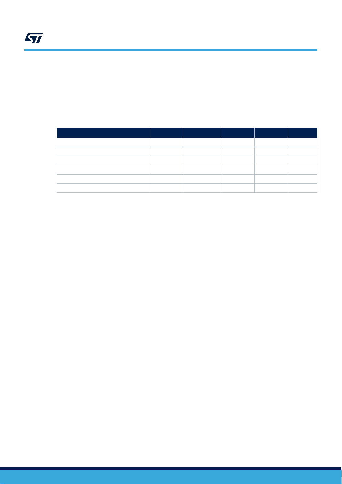
The power MOSFETs integrated into the powerSTEP01 system-in-package has a total gate charge of 25 nC
(typical) and the recommended configurations are listed in Table 6.
Table 6. Recommended gate driving configurations
Slew rate (VS = 48 V) Igate tCC tDT tblank tboost
980 V/µs 96 mA 375 ns 125 ns 500 ns 0 ns
790 V/µs 64 mA 500 ns 125 ns 375 ns 0 ns
520 V/µs 32 mA 875 ns 125 ns 250 ns 0 ns
400 V/µs 24 mA 1000 ns 125 ns 250 ns 0 ns
220 V/µs 16 mA 1600 ns 125 ns 250 ns 0 ns
114 V/µs 8 mA 3125 ns 125 ns 250 ns 0 ns
Important: An incorrect gate driving setup may cause spurious overcurrent failures, even if no load is connected to the
power stage.
The suggested configuration for the demonstration board is the following:
• VCC = 15 V
• UVLO protection threshold set high (UVLOVAL = '1')
• Gate current = 64 mA
• Controlled current time = 500 ns
• Deadtime = 125 ns
• Blanking time = 375 ns
• Turn OFF boost time = disabled
3.4 Overcurrent and stall detection thresholds
The overcurrent protection and the stall detection are implemented measuring the drain source voltage of the
MOSFETs, hence their value is a voltage and not a current.
The protection thresholds are set according to the voltage drop caused by the target triggering current on the
MOSFET RDS(on) at the expected operating temperature (in fact, these parameters increase with temperature).
During the preliminary stages of evaluation, the max. value of 1000 mV can be set for both protections. The
default value of 281.25 mV has a good probability to trigger the overcurrent alarm.
Important: It is strongly discouraged to disable the overcurrent shutdown; it may result in critical failures.
3.5 Speed profile
The max. speed parameter is the maximum speed the motor will run. By default, it is about 1000 step/s. That
means, if you send a command to run at 2000 step/s, the motor speed it limited at 1000 step/s.
This is an important safety feature in the final application, but not necessarily useful to evaluate the device
performances. Setting the parameter to high values (e.g., 6000 step/s) allows evaluating the maximum speed
which can be achieved by the application under test through the speed tracking command (Run), but it probably
limits the possibility to use positioning commands (Move, GoTo, etc.).
The Full-Step speed parameter indicates the speed at which the system switches from microstepping to full
step operation.
In voltage mode driving, it is always recommended to operate in microstepping and not to switch to the full step.
Hence, this parameter should be greater than the maximum speed.
UM1829
Gate drivers
UM1829 - Rev 2 page 10/21

4Sensing resistors
In the advanced current control mode, the output current range is determined by the sensing resistors as
indicated in the following formulas:
Ipeak,min =7.8mV
Rsense (2)
Ipeak,max =1V
Rsense (3)
Where 7.8 mV and 1 V are the minimum and the maximum value of the TVAL registers.
However, the actual output current is usually limited by the power rating of the sensing resistors:
Iout,limit =Pd,max
Rsense rmsvalue (4)
Note: The power rating of the sensing resistor determining the maximum output current is 50% of the nominal one.
If the operative range resulting from the sensing resistors which are mounted on the board is not suitable for the
application, it is possible to change these components in order to fit the requirements.
The sensing resistors should make the current control operates with a peak reference voltage between 0.2 and
0.1 volts. This way, the power dissipation on the sensing resistor is not excessive and the offset of the sensing
circuitry does not affect the performance of the current control algorithm.
Rsense =0.2V
Ipeak (5)
UM1829
Sensing resistors
UM1829 - Rev 2 page 11/21

5How to change the supply configuration of the board
The configuration of the supply voltages can be changed through the jumpers from J3 to J8 as listed in Table 7,
Table 8 and Table 9.
Table 7. VCC supply configurations
Configuration JP3 JP4 VSREG range Notes
Internally generated from VS Closed Open VCC + 3 V to 85 V
Default.
VCC value is determined by the internal regulator
configuration.
Internally generated from a
voltage source different from VS Open Open VCC + 3 V to VS
VCC value is determined by the internal regulator
configuration.
External protection diode could be required (see
following).
Externally supplied (equal to
VSREG) Open Closed 7.5 V to 15 V External protection diode could be required (see
following).
Note: When the VCC voltage of 7.5 V is used, the charge pump diodes should be replaced with low drop ones
(suggested part BAR43SFILM). Otherwise, the resulting boot voltage could be lower than the respective UVLO
threshold and the device is not operative.
When the VSREG pin is not shorted to VS (JP1 is open), particular care must be taken in order to avoid that
the VBOOT voltage falls below the VSREG one (e.g., VS is floating and VSREG is supplied). If this occurs, the
internal ESD diode is turned on and the device could be damaged. Adding a low drop diode between VSREG and
VS protects the internal ESD diode from this event (the charge pump diodes must also be low drop type).
Table 8. VREG supply configurations
Configuration JP5 JP6 VCCREG range Notes
Internally generated from VCC Closed Open VCC Default.
Internally generated from a voltage source
different from VCC Open Open 6.3 V to VCC External protection diode could be
required (see following).
Externally supplied (equal to VCCREG) Open Closed 3.3 V External protection diode could be
required (see following).
When the VCCREG pin is not shorted to VCC (JP3 is open), particular care must be taken to avoid that the VCC
voltage falls below the VCCREG one. If this occurs, the internal ESD diode is turned on and the device could be
damaged. Adding a low drop diode between VCCREG and VCC protects the internal ESD diode from this event.
Table 9. VDD supply configurations
Configuration JP7 JP8 VDD range Notes
Supplied by VREG Closed Open 3.3 V Default, 3.3 V logic.
Supplied by SPI connectors Open Closed 3.3 V or 5 V 3.3 V when connected to the STEVAL-PCC009V2.
Supplied by VDD test point Open Open 3.3 V or 5 V Must be 3.3 V if connected to the STEVAL-PCC009V2.
UM1829
How to change the supply configuration of the board
UM1829 - Rev 2 page 12/21

6Daisy chaining
More demonstration boards can be connected in the daisy chain mode. To drive two or more boards in daisy
chain configuration:
1. Connect the STEVAL-PCC009V2 board 10-pin connector to the SPI_IN connector of the first demonstration
board through the 10-pole flat cable.
2. Open the termination jumper (see Section 3.1 and Section 3.2 ).
3. Connect the SPI_OUT connector of the first demonstration board to the SPI_IN of the next one through the
10-pole flat cable.
4. Repeat point 2 and 3 for all the others board of the chain but the last one.
5. Check the termination jumpers of the demonstration boards: all the jumpers except the last one should be
opened.
Note: Increasing the number of devices connected in the chain could degrade SPI communication performances. If
communication issues occur, try reducing the SPI clock speed.
UM1829
Daisy chaining
UM1829 - Rev 2 page 13/21

7EVLPOWERSTEP01 transient thermal analysis
Test setup:
• Supply voltage VS = 24 V
• Load RL type: R = 3.5 Ω, L = 400 μH for each phase
• Load current 3.5 Arms for each phase (4.2 Apeak)
• The powerSTEP01 is working in full-step mode
Figure 5. PowerSTEP01 register map
UM1829
EVLPOWERSTEP01 transient thermal analysis
UM1829 - Rev 2 page 14/21

Figure 6. powerSTEP01 full-step phase currents
Measured data:
• Ambient and Junction temperature
• Device power dissipation (PDUT ≅ 1.5 W)
Ztℎt=Tj− Tamb
PDUT (6)
Figure 7. EVLPOWERSTEP01 transient thermal impedance
0
2
4
6
8
10
12
14
16
0.1 1 10 100 1000 10000
Zth [°C/W]
Time [s]
Note: The normalized chart is independent from the currents and dissipated power.
UM1829
EVLPOWERSTEP01 transient thermal analysis
UM1829 - Rev 2 page 15/21

Assuming a maximum junction temperature of 150°C, the power dissipation curve is shown in the following figure.
Figure 8. EVLPOWERSTEP01 power dissipation curve
0
2
4
6
8
10
0 20 40 60 80 100 120 140 160
Power dissipation [W]
Temperature [°C]
Note: All the results are board-specific.
UM1829
EVLPOWERSTEP01 transient thermal analysis
UM1829 - Rev 2 page 16/21

Contents
1Board description .................................................................2
1.1 EVLPOWERSTEP01 schematics .................................................4
1.2 EVLPOWERSTEP01 Bill of materials..............................................6
2Evaluation environment setup .....................................................8
3Device configuration...............................................................9
3.1 Voltage mode driving ...........................................................9
3.2 Advanced current control ........................................................9
3.3 Gate drivers ..................................................................10
3.4 Overcurrent and stall detection thresholds.........................................10
3.5 Speed profile .................................................................10
4Sensing resistors.................................................................11
5How to change the supply configuration of the board .............................12
6Daisy chaining....................................................................13
7EVLPOWERSTEP01 transient thermal analysis ....................................14
Revision history .......................................................................17
UM1829
Contents
UM1829 - Rev 2 page 18/21

List of figures
Figure 1. EVLPOWERSTEP01 evaluation board ...................................................1
Figure 2. EVLPOWERSTEP01 jumper and connector locations .........................................2
Figure 3. EVLPOWERSTEP01 schematic 1 of 2....................................................4
Figure 4. EVLPOWERSTEP01 schematic 2 of 2....................................................5
Figure 5. PowerSTEP01 register map .......................................................... 14
Figure 6. powerSTEP01 full-step phase currents .................................................. 15
Figure 7. EVLPOWERSTEP01 transient thermal impedance .......................................... 15
Figure 8. EVLPOWERSTEP01 power dissipation curve.............................................. 16
UM1829
List of figures
UM1829 - Rev 2 page 19/21

List of tables
Table 1. EVLPOWERSTEP01 electrical specifications ................................................2
Table 2. Jumpers and connectors description ......................................................2
Table 3. Master SPI connector pinout (J5) .........................................................3
Table 4. Slave SPI connector pinout (J7)..........................................................3
Table 5. Bill of materials .....................................................................6
Table 6. Recommended gate driving configurations ................................................. 10
Table 7. VCC supply configurations ............................................................ 12
Table 8. VREG supply configurations ........................................................... 12
Table 9. VDD supply configurations ............................................................ 12
Table 10. Document revision history ............................................................. 17
UM1829
List of tables
UM1829 - Rev 2 page 20/21
Table of contents
Other ST Motherboard manuals

ST
ST STEVAL-IHM022V1 User manual

ST
ST STM32H735G-DK User manual

ST
ST EVAL-L99DZ200 User manual

ST
ST STM3240G-EVAL User manual

ST
ST NUCLEO-F207ZG User manual

ST
ST UM1932 User manual

ST
ST STM32H757I-EVAL User manual

ST
ST STEVAL-IHM011V1 User manual

ST
ST STEVAL-IPE005V1 User manual

ST
ST STA333ML Installation and operating instructions

ST
ST eMotion STEVAL-MKI109V1 User manual

ST
ST STEVAL-BLUEPIRV1 User manual

ST
ST STEVAL-OET001V1 User manual

ST
ST AEK-MOT-TK200G1 User manual

ST
ST UM1461 User manual

ST
ST EVAL-L9963-MCU Installation and operating instructions

ST
ST B-L4S5I-IOT01A User manual

ST
ST ARMIC30 User manual

ST
ST ST25DV-I2C User manual

ST
ST FDA803S User manual