5Power and system configuration
5.1 Power supplies
The mini module can be powered by providing the three voltages (5 V, 3.3 V and 1.25 V) or supplied externally by
the 4 pins connector (J5) or supplied by the motherboard.
When the mini module is plugged onto the motherboard, power is supplied directly by the motherboard. In this
setup, the external power supply input available on the mini module should NOT be used.
When the SPC58XXADPT176S Rev. B mini module is used as a stand-alone board, external power supplies
must be used (5 V, 3.3 V, 1.25 V).
The following jumpers are used to configure the power supply (common for all supported devices):
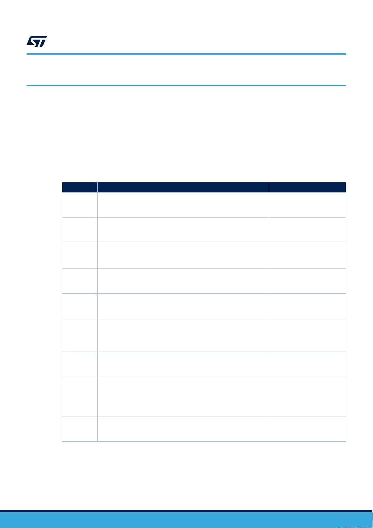
Table 1. Power configuration jumpers
Jumper Description Default
J1
VDD_HV_ADR voltage configuration:
• 1-2 5.0V_LR
• 2-3 3.3V_SR
1-2
(5.0V_LR)
J2
VDD_HV_ADV voltage configuration:
• 1-2 5.0V_LR
• 2-3 3.3V_SR
1-2
(5.0V_LR)
J3
VDD_HV_IO_JTAG voltage configuration:
• 1-2 5.0V_SR
• 2-3 3.3V_SR
1-2
(5.0V_SR)
J6
VDD_HV_IO_MAIN voltage configuration:
• 1-2 5.0V_SR
• 2-3 3.3V_SR
1-2
(5.0V_SR)
J7
VDD_HV_IO_FLEX voltage configuration:
• 1-2 5.0V_SR
• 2-3 3.3V_SR
1-2
(5.0V_SR)
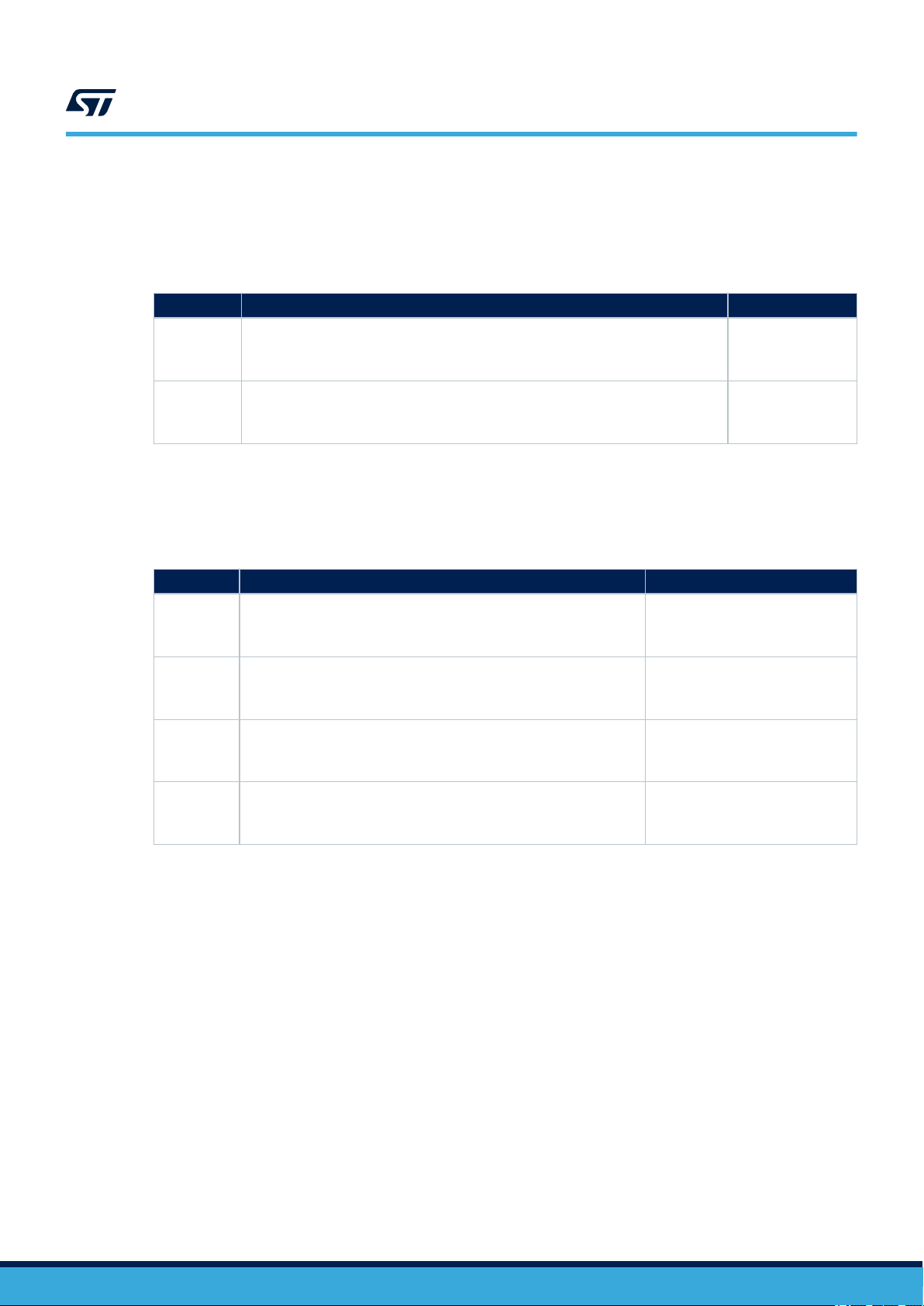
J38
Device pin 153 EXTREG_SEL function configuration:
• 2-1 Reserved for STMicroelectronics
• 2-3 ENABLED BALLAST
• 2-4 DISABLE BALLAST
2-4
(DISABLE BALLAST)
J39
Supply for BALLAST circuit configuration
• 1-2 VDD_HV_IO_MAIN
• 2-3 5.0V_SR
1-2
(VDD_HV_IO_MAIN)
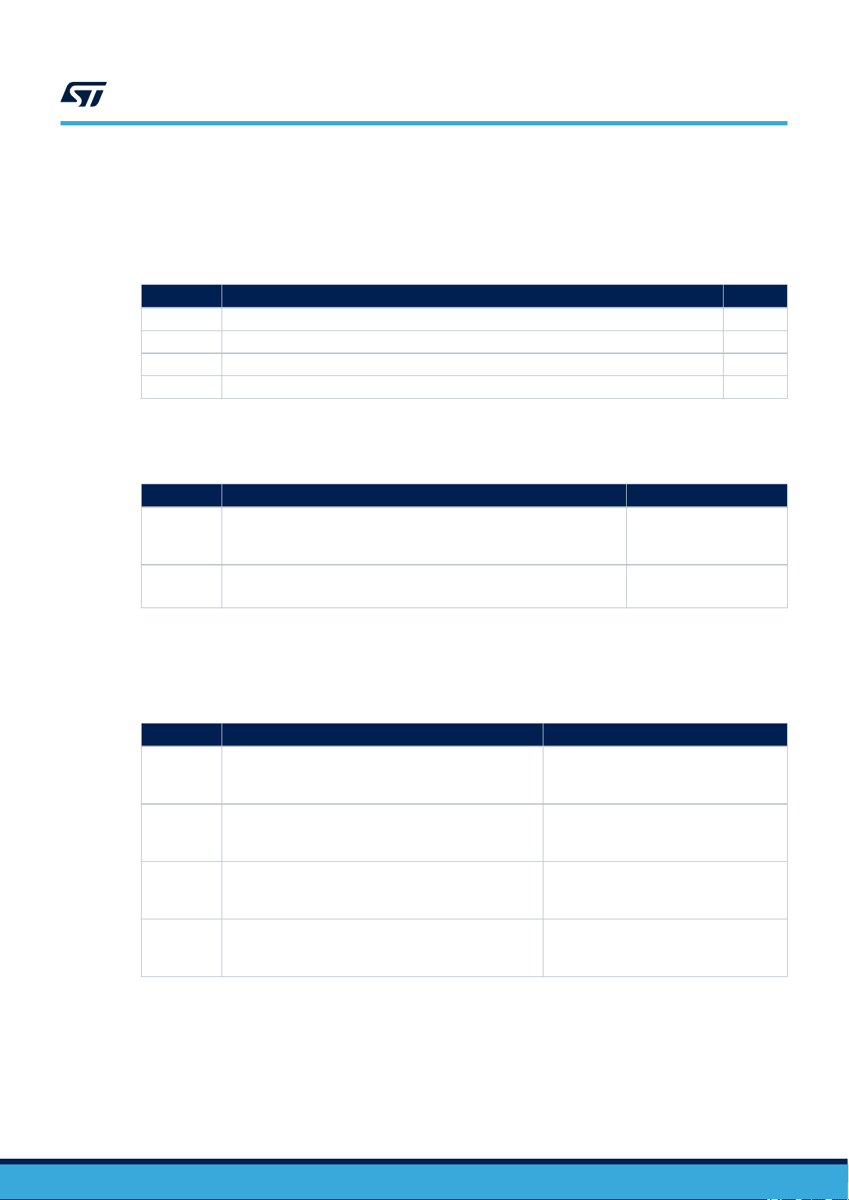
J40
VDD_LV voltage configuration:
• 2-1 (BALLAST circuit)
• 2-3 (1.25V_SR)
• 2-4 (SMPS regulator module) Do not use this configuration for
SP58xG8xE7
2-3
(1.25V_SR)
J43
Device pin 155 VDD_HV_FLA voltage configuration:
• OPEN – disconnect VDD_HV_FLA from VDD_HV_IO_MAIN
• CLOSED - connect VDD_HV_FLA from VDD_HV_IO_MAIN
Closed
(connect pin 155 VDD_HV_FLA
to VDD_HV_IO_MAIN)
UM2723
Power and system configuration
UM2723 - Rev 1 page 7/28