ST UM1932 User manual

September 2015 DocID028183 Rev 1 1/40
1
UM1932
User Manual
Discovery kit with STM32F469NI MCU
Introduction
The STM32F469I-DISCO discovery board (32F469IDISCOVERY) is a complete
demonstration and development platform for STMicroelectronics ARM®Cortex® -M4 core-
based STM32F469NIH6 microcontroller. This microcontroller features three I2C interfaces,
six SPIs with two multiplexed full-duplex I2S interfaces, SDIO, four USARTs, four UARTs,
two CANs, three 12-bit ADCs, two 12-bit DACs, one SAI, 8 to 14-bit digital camera digital
module interface, internal 320+4 Kbytes of SRAM and 2-Mbyte Flash memory, USB HS
OTG and USB FS OTG, Ethernet MAC, FMC interface, MIPI DSI interface, Quad-SPI
interface, JTAG debugging support. This discovery board offers everything required for
users to get started quickly and develop applications easily.
The hardware features on the board helps users to evaluate the following peripherals: USB
OTG FS, microSD card, Audio DAC with headset jack, digital microphones, SDRAM, Quad-
SPI Flash memory, 4" TFT LCD using MIPI DSI interface with capacitive touch panel.The
Arduino™compatible connectors expand the functionality with a wide choice of specialized
shields.The extension header makes it possible to easily connect a daughterboard for
specific application. The integrated ST-LINK/V2-1 provides an embedded in-circuit
debugger and programmer for the STM32 MCU.
Figure 1. STM32F469I-DISCO board (top view)
Figure 2. STM32F469I-DISCO board (bottom view)
1. Pictures not contractual.
www.st.com

Contents UM1932
2/40 DocID028183 Rev 1
Contents
1 Features . . . . . . . . . . . . . . . . . . . . . . . . . . . . . . . . . . . . . . . . . . . . . . . . . . . 6
2 Demonstration software . . . . . . . . . . . . . . . . . . . . . . . . . . . . . . . . . . . . . . 7
3 Order code . . . . . . . . . . . . . . . . . . . . . . . . . . . . . . . . . . . . . . . . . . . . . . . . . 7
4 Technology Partners . . . . . . . . . . . . . . . . . . . . . . . . . . . . . . . . . . . . . . . . . 7
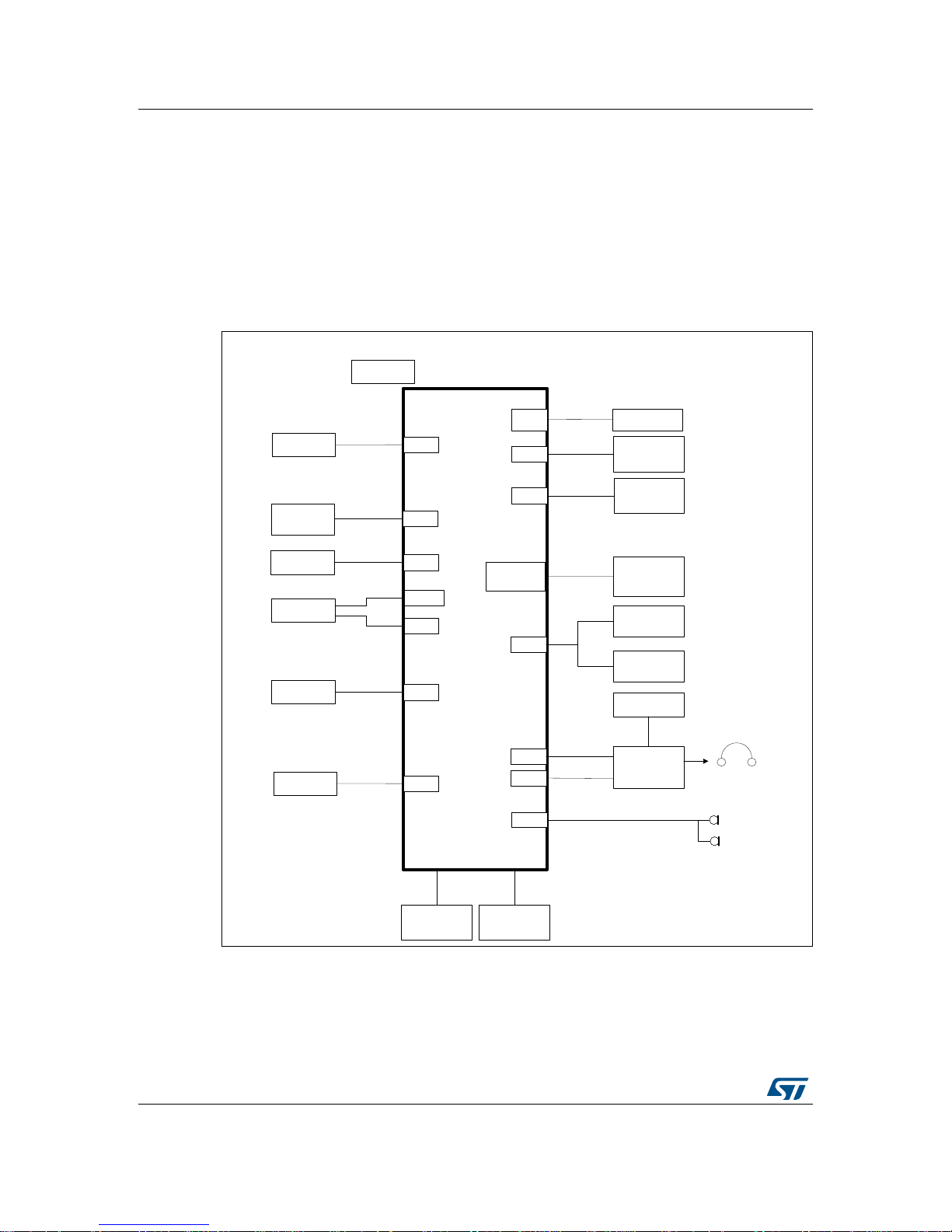
5 Hardware layout and configuration . . . . . . . . . . . . . . . . . . . . . . . . . . . . . 8
5.1 Embedded ST-LINK/V2-1 . . . . . . . . . . . . . . . . . . . . . . . . . . . . . . . . . . . . . .11
5.1.1 Drivers . . . . . . . . . . . . . . . . . . . . . . . . . . . . . . . . . . . . . . . . . . . . . . . . . . 11
5.1.2 ST-LINK/V2-1 firmware upgrade . . . . . . . . . . . . . . . . . . . . . . . . . . . . . . 11
5.2 Power supply . . . . . . . . . . . . . . . . . . . . . . . . . . . . . . . . . . . . . . . . . . . . . . 12
5.2.1 Power supply sources . . . . . . . . . . . . . . . . . . . . . . . . . . . . . . . . . . . . . . 12
5.2.2 Supplying the board through ST-LINK/V2-1 USB port . . . . . . . . . . . . . . 12
5.2.3 Measurement of current IDD drawn by the STM32F469NI . . . . . . . . . 13
5.2.4 Power related jumpers . . . . . . . . . . . . . . . . . . . . . . . . . . . . . . . . . . . . . . 13
5.3 Clock source . . . . . . . . . . . . . . . . . . . . . . . . . . . . . . . . . . . . . . . . . . . . . . . 14
5.3.1 HSE clock source . . . . . . . . . . . . . . . . . . . . . . . . . . . . . . . . . . . . . . . . . 14
5.3.2 LSE clock source . . . . . . . . . . . . . . . . . . . . . . . . . . . . . . . . . . . . . . . . . . 14
5.4 Reset source . . . . . . . . . . . . . . . . . . . . . . . . . . . . . . . . . . . . . . . . . . . . . . 15
5.5 Audio outputs . . . . . . . . . . . . . . . . . . . . . . . . . . . . . . . . . . . . . . . . . . . . . . 15
5.6 Digital microphones . . . . . . . . . . . . . . . . . . . . . . . . . . . . . . . . . . . . . . . . . 15
5.7 USB OTG FS . . . . . . . . . . . . . . . . . . . . . . . . . . . . . . . . . . . . . . . . . . . . . . 15
5.8 MicroSD card . . . . . . . . . . . . . . . . . . . . . . . . . . . . . . . . . . . . . . . . . . . . . . 16
5.9 SDRAM . . . . . . . . . . . . . . . . . . . . . . . . . . . . . . . . . . . . . . . . . . . . . . . . . . 16
5.10 Quad-SPI NOR Flash Memory . . . . . . . . . . . . . . . . . . . . . . . . . . . . . . . . . 16
5.11 Virtual ComPort . . . . . . . . . . . . . . . . . . . . . . . . . . . . . . . . . . . . . . . . . . . . 16
5.12 Arduino connectors . . . . . . . . . . . . . . . . . . . . . . . . . . . . . . . . . . . . . . . . . 16
5.13 Extension connector CN12 . . . . . . . . . . . . . . . . . . . . . . . . . . . . . . . . . . . . 18
5.14 DSI LCD . . . . . . . . . . . . . . . . . . . . . . . . . . . . . . . . . . . . . . . . . . . . . . . . . . 21
5.15 Buttons and LEDs . . . . . . . . . . . . . . . . . . . . . . . . . . . . . . . . . . . . . . . . . . 22
5.16 I2C extension connector CN11 . . . . . . . . . . . . . . . . . . . . . . . . . . . . . . . . . 23

DocID028183 Rev 1 3/40
UM1932 Contents
3
5.17 USB OTG FS Micro-AB connector CN13 . . . . . . . . . . . . . . . . . . . . . . . . . 23
5.18 MicroSD connector CN9 . . . . . . . . . . . . . . . . . . . . . . . . . . . . . . . . . . . . . . 24
5.19 ST-LINK/V2-1 USB Mini Type B connector CN1 . . . . . . . . . . . . . . . . . . . 24
5.20 Audio jack CN3 . . . . . . . . . . . . . . . . . . . . . . . . . . . . . . . . . . . . . . . . . . . . . 25
6 Schematics . . . . . . . . . . . . . . . . . . . . . . . . . . . . . . . . . . . . . . . . . . . . . . . 26
Appendix A Mechanical dimensions. . . . . . . . . . . . . . . . . . . . . . . . . . . . . . . . . . . 38
7 Revision History . . . . . . . . . . . . . . . . . . . . . . . . . . . . . . . . . . . . . . . . . . . 39

List of tables UM1932
4/40 DocID028183 Rev 1
List of tables
Table 1. Power related jumpers . . . . . . . . . . . . . . . . . . . . . . . . . . . . . . . . . . . . . . . . . . . . . . . . . . . . 13
Table 2. Arduino compatible connectors . . . . . . . . . . . . . . . . . . . . . . . . . . . . . . . . . . . . . . . . . . . . . 17
Table 3. Arduino compatible connectors . . . . . . . . . . . . . . . . . . . . . . . . . . . . . . . . . . . . . . . . . . . . . 18
Table 4. Extension connector pinout . . . . . . . . . . . . . . . . . . . . . . . . . . . . . . . . . . . . . . . . . . . . . . . . 20
Table 5. DSI LCD module connector (CN10) . . . . . . . . . . . . . . . . . . . . . . . . . . . . . . . . . . . . . . . . . . 21
Table 6. Port assignment for control of LED indicators . . . . . . . . . . . . . . . . . . . . . . . . . . . . . . . . . . 22
Table 7. I2C extension connector pinout . . . . . . . . . . . . . . . . . . . . . . . . . . . . . . . . . . . . . . . . . . . . . 23
Table 8. USB OTG FS Micro-AB connector CN13 . . . . . . . . . . . . . . . . . . . . . . . . . . . . . . . . . . . . . . 23
Table 9. MicroSD connector CN9. . . . . . . . . . . . . . . . . . . . . . . . . . . . . . . . . . . . . . . . . . . . . . . . . . . 24
Table 10. USB Mini type B connector CN1. . . . . . . . . . . . . . . . . . . . . . . . . . . . . . . . . . . . . . . . . . . . . 25
Table 11. Document Revision History . . . . . . . . . . . . . . . . . . . . . . . . . . . . . . . . . . . . . . . . . . . . . . . . 39

DocID028183 Rev 1 5/40
UM1932 List of figures
5
List of figures
Figure 1. STM32F469I-DISCO board (top view) . . . . . . . . . . . . . . . . . . . . . . . . . . . . . . . . . . . . . . . . . 1
Figure 2. STM32F469I-DISCO board (bottom view) . . . . . . . . . . . . . . . . . . . . . . . . . . . . . . . . . . . . . . 1
Figure 3. Hardware Block Diagram . . . . . . . . . . . . . . . . . . . . . . . . . . . . . . . . . . . . . . . . . . . . . . . . . . . 8
Figure 4. STM32F469I-DISCO top side layout . . . . . . . . . . . . . . . . . . . . . . . . . . . . . . . . . . . . . . . . . . 9
Figure 5. STM32F469I-DISCO bottom side layout . . . . . . . . . . . . . . . . . . . . . . . . . . . . . . . . . . . . . . 10
Figure 6. USB Composite device. . . . . . . . . . . . . . . . . . . . . . . . . . . . . . . . . . . . . . . . . . . . . . . . . . . . 11
Figure 7. Extension connector CN12. . . . . . . . . . . . . . . . . . . . . . . . . . . . . . . . . . . . . . . . . . . . . . . . . 19
Figure 8. I2C extension connector (front view) . . . . . . . . . . . . . . . . . . . . . . . . . . . . . . . . . . . . . . . . . 23
Figure 9. USB OTG FS Micro-AB connector CN13 (front view). . . . . . . . . . . . . . . . . . . . . . . . . . . . . 23
Figure 10. MicroSD connector CN9 (front view) . . . . . . . . . . . . . . . . . . . . . . . . . . . . . . . . . . . . . . . . . 24
Figure 11. USB type Mini B connector CN1 (front view) . . . . . . . . . . . . . . . . . . . . . . . . . . . . . . . . . . . 24
Figure 12. STM32F469I-DISCO Discovery board . . . . . . . . . . . . . . . . . . . . . . . . . . . . . . . . . . . . . . . . 26
Figure 13. STM32F469I-DISCO MCU . . . . . . . . . . . . . . . . . . . . . . . . . . . . . . . . . . . . . . . . . . . . . . . . 27
Figure 14. Extension connectors . . . . . . . . . . . . . . . . . . . . . . . . . . . . . . . . . . . . . . . . . . . . . . . . . . . . . 28
Figure 15. Power . . . . . . . . . . . . . . . . . . . . . . . . . . . . . . . . . . . . . . . . . . . . . . . . . . . . . . . . . . . . . . . . . 29
Figure 16. Peripherals . . . . . . . . . . . . . . . . . . . . . . . . . . . . . . . . . . . . . . . . . . . . . . . . . . . . . . . . . . . . . 30
Figure 17. Audio codec and microphone MEMS . . . . . . . . . . . . . . . . . . . . . . . . . . . . . . . . . . . . . . . . . 31
Figure 18. 4-inch DSI LCD board. . . . . . . . . . . . . . . . . . . . . . . . . . . . . . . . . . . . . . . . . . . . . . . . . . . . . 32
Figure 19. SDRAM. . . . . . . . . . . . . . . . . . . . . . . . . . . . . . . . . . . . . . . . . . . . . . . . . . . . . . . . . . . . . . . . 33
Figure 20. QSPI . . . . . . . . . . . . . . . . . . . . . . . . . . . . . . . . . . . . . . . . . . . . . . . . . . . . . . . . . . . . . . . . . . 34
Figure 21. USB OTG FS . . . . . . . . . . . . . . . . . . . . . . . . . . . . . . . . . . . . . . . . . . . . . . . . . . . . . . . . . . . 35
Figure 22. Arduino UNO connector . . . . . . . . . . . . . . . . . . . . . . . . . . . . . . . . . . . . . . . . . . . . . . . . . . . 36
Figure 23. ST-LINK/V2-1 . . . . . . . . . . . . . . . . . . . . . . . . . . . . . . . . . . . . . . . . . . . . . . . . . . . . . . . . . . . 37
Figure 24. Mechanical dimensions in millimeter . . . . . . . . . . . . . . . . . . . . . . . . . . . . . . . . . . . . . . . . . 38

Features UM1932
6/40 DocID028183 Rev 1
1 Features
•STM32F469NIH6 microcontroller featuring 2 Mbytes of Flash memory and 324 Kbytes
of RAM in BGA216 package
•On-board ST-LINK/V2-1 SWD debugger, supporting USB reenumeration capability:
– Mbed-enabled (mbed.org)
– USB functions: USB virtual COM port, mass storage, debug port
•4-inch 800x480 pixel TFT color LCD with MIPI DSI interface and capacitive touch
screen
•SAI Audio DAC, with a stereo headphone output jack
•Three MEMS microphones
•MicroSD card connector
•I2C extension connector
•4Mx32bit SDRAM
•128-Mbit Quad-SPI NOR Flash
•Reset and wake-up buttons
•4 color user LEDs
•USB OTG FS with Micro-AB connector
•Three power supply options:
– ST-LINK/V2-1 USB connector
– User USB FS connector
– VIN from Arduino™ compatible connectors
•Expansion connectors and Arduino™ UNO V3 connectors
•Comprehensive free software including a variety of examples, part of STM32Cube
package
•Supported by a wide choice of integrated development environments

DocID028183 Rev 1 7/40
UM1932 Demonstration software
39
2 Demonstration software
The demonstration software is preloaded in the STM32F469NIH6 Flash memory and in the
MICRON N25Q128A NOR Flash memory. The latest version of the demonstration source
code and associated documentation can be downloaded from
www.st.com/stm32f4discovery.
3 Order code
To order the Discovery kit based on the STM32F469NI MCU, use the order code:
STM32F469I-DISCO.
4 Technology Partners
MICRON:
•128-Mbit SDRAM device, part number MT48LC4M32B2
•128-Mbit Quad-SPI NOR Flash memory device, part number N25Q128A

Hardware layout and configuration UM1932
8/40 DocID028183 Rev 1
5 Hardware layout and configuration
STM32F469I-DISCO evaluation board is designed around the STM32F469NIH6 (216-pin
TFBGA package). The Figure 3 illustrates the connection between STM32F469NIH6 and
peripherals (SDRAM, Quad-SPI Flash memory, Color LCD, USB OTG connector, Audio,
I2C extension connector, microSD card and embedded ST-LINK). Figure 4: STM32F469I-
DISCO top side layout and Figure 5: STM32F469I-DISCO bottom side layout will help to
locate these features on the actual evaluation board.
Figure 3. Hardware Block Diagram
670)1,+
%*$SDFNDJH
$XGLR&2'(&
57&
93RZHU
6XSSO\
.+]&U\VWDO
[/('V
67/,1.9
,&
6$,
,&H[WHQVLRQ
FRQQHFWRU
'6,/&'
0LFUR6'FDUG
FRQQHFWRU
:DNHXSEXWWRQ*3,2
3RWHQWLRPHWHU$'&
6',2
)0&0E6'5$0
463,
0E4XDG
63,)ODVK
PHPRU\
27*
)6 86%FRQQHFWRU
86$57
0,3,'6,
93RZHU
6XSSO\
*3,2V
6:'
6WHUHRKHDGSKRQH
RXWSXW
6WHUHRGLJLWDO
PLFURSKRQHV
63,
/&'7RXFK
SDQHO
$UGXLQR
FRQQHFWRU
([WHQVLRQ
FRQQHFWRU
,&
06Y9

DocID028183 Rev 1 9/40
UM1932 Hardware layout and configuration
39
Figure 4. STM32F469I-DISCO top side layout
06Y9
/'
9%86/('
/'/'/'/'
*UHHQ2UDQJH5HG%OXH
/('VUHVSHFWLYHO\
8
'LJLWDO
PLFURSKRQH
==
LQFKHV'6,
/&'
/'
9
%86/(
'
8
'LJLWDO
PLFURSKRQH
6%
6ROGHU
EULGJH
6%
6ROGHU
EULGJH
8
'LJLWDO
PLFURSKRQH
/'
9%86/('

Hardware layout and configuration UM1932
10/40 DocID028183 Rev 1
Figure 5. STM32F469I-DISCO bottom side layout
06Y9
%
:DNHXS
EXWWRQ
%
5HVHWEXWWRQ
&1
67/,1.9
86%
-3
3RZHU
VHOHFWLRQ
MXPSHU
/'
67/,1.9
&20/('
&1&1
&1&1
$UGXLQR
&RQQHFWRUV
&1
([WHQVLRQ
&RQQHFWRU
&1
86%27*
)6
&RQQHFWRU
&1
PLFUR6'
FDUG
&1
,&
H[WHQVLRQ
FRQQHFWRU
-3
,''FXUUHQW
PHDVXUHPHQW
MXPSHU
8
670)1,+
&1
$XGLRMDFN
/'
9/('

DocID028183 Rev 1 11/40
UM1932 Hardware layout and configuration
39
5.1 Embedded ST-LINK/V2-1
The ST-LINK/V2-1 programming and debugging tool is integrated on the STM32469I-
DISCO board. Compared to ST-LINK/V2 the new features supported on ST-LINK/V2-1 are:
•USB software re-enumeration
•Virtual com port interface on USB
•Mass storage interface on USB
•USB power management request for more than 100mA power on USB
This feature is no more supported on ST-LINK/V2-1:
•SWIM interface
For all general information concerning debugging and programming features common
between V2 and V2-1 please refer to ST-LINK/V2 User Manual UM1075.
5.1.1 Drivers
Before connecting STM32F469I-DISCO board to a Windows 7, Windows 8 or Windows XP
PC via USB, a driver for ST-LINK/V2-1 must be installed. It can be downloaded from
www.st.com.
In case the STM32F469I-DISCO board is connected to the PC before installing the driver,
the Windows device manager may report some USB devices found on STM32F469I-DISCO
as “Unknown”. To recover from this situation, after installing the dedicated driver
downloaded from www.st.com, the association of “Unknown” USB devices found on
STM32F469I-DISCO to this dedicated driver must be updated in the device manager
manually. It is recommended to proceed using USB Composite Device line, as shown in
figure below
Note: Prefer using the “USB Composite Device” handle for a full recovery.
Figure 6. USB Composite device
5.1.2 ST-LINK/V2-1 firmware upgrade
ST-LINK/V2-1 facility for debug and flashing of the target microcontroller STM32F469NIH6
is integrated on STM32F469I-DISCO board. For its own operation, ST-LINK/V2-1 employs a
dedicated MCU with Flash memory. Its firmware determines ST-LINK/V2-1 functionality and
performance. The firmware may evolve during the life span of STM32F469I-DISCO to
include new functionality, fix bugs or support new target microcontroller families. It is

Hardware layout and configuration UM1932
12/40 DocID028183 Rev 1
therefore recommended to keep ST-LINK/V2-1 firmware up to date. The latest version is
available from www.st.com. ST-LINK/V2-1 supports a mechanism that allows flashing its
dedicated MCU via the USB interface on the hosting board, here STM32F469I-DISCO. The
whole process is controlled from a Windows PC application also available from www.st.com.
5.2 Power supply
5.2.1 Power supply sources
STM32F469I-DISCO board is designed to be powered by the following sources:
•5 V DC from the ST-LINK/V2-1 USB connector CN1 with 500 mA current limitation.
Power mechanism of the board supplied by the USB ST-LINK/V2-1 is explained below
(Section 5.2.2: Supplying the board through ST-LINK/V2-1 USB port). Pins 3 and 4 of
jumper JP2 should be closed by placing a jumper in location called STLK on silkscreen
of the board. Jumper JP5 should be closed.The red LED LD5 is lighted on to confirm
the presence of +5 V voltage.
•5 V DC from the user USB FS connector CN13. Pins 5 and 6 of jumper JP2 should be
closed by placing a jumper in location called USB on silkscreen of the board. Jumper
JP5 should be closed. The red LED LD5 is lighted on to confirm the presence of +5 V
voltage.
•6 V to 9 V DC from VIN pin of Arduino™compatible connector CN6. The voltage must
be limited to 9 V to keep the temperature of the regulator U10 within its thermal safe
area. Pins 1 and 2 of jumper JP2 should be closed by placing a jumper in location
called E5V on silkscreen of the board. Jumper JP5 should be closed. The red LED LD5
is lighted on to confirm the presence of +5 V voltage.
•An external +3.3 V DC source connected to pin 4 of Arduino™compatible connector
CN6. The user should carefully check that the voltage of the external supply is +3.3 V
before connecting to pin 4 of CN6, since this voltage is directly applied to supply pins of
the microcontroller. Jumper JP5 should be closed, and it is mandatory to remove the
solder bridge SB8, to avoid applying a reverse current to the output of regulator U7.
The LED LD5 is not lighted because it is not connected to +3.3 V supply. No jumper in
JP2. Using this power scheme, the USB host mode and LCD backlight do not work
because the 5 V is not available.
•An external +3.3 V DC source connected to pin 1 of extension connector CN12.The
user should carefully check that the voltage of the external supply is +3.3 V before
connecting to pin 1 of CN12, since this voltage is directly applied to supply pins of the
microcontroller. Jumper JP5 should be closed, and it is mandatory to remove the solder
bridge SB8 to avoid to apply a reverse current to the output of regulator U7. The LED
LD5 is not lighted because not connected to +3.3 V supply. No jumper in JP2. Using
this power scheme, the USB host mode and LCD backlight do not work because the
5 V is not available.
5.2.2 Supplying the board through ST-LINK/V2-1 USB port
To power the STM324F69I-DISCO board in this way, the USB host (a PC) gets connected
with the STM324F69I-DISCO board via USB cable to ST-LINK/V2-1 connector.
In the first step, only the ST-LINK part U3 is powered by the PC. In fact, before USB
enumeration the host PC provides only 100mA to the board at that time. STM324F69I-
DISCO board requests for 500mA power to the host PC. If the host is able to provide the

DocID028183 Rev 1 13/40
UM1932 Hardware layout and configuration
39
required power, the enumeration finishes by a “SetConfiguration” command and then, the
power switch ST890 U4 is switched ON, the red LED LD5 is turned ON, thus the board can
consume no more than 500mA. If the host is not able to provide such requested current, the
enumeration fails. Therefore the ST890 U4 remains OFF and the board will not be powered.
As a consequence the red LED LD5 remains turned OFF. In this case it is mandatory to use
another power supply source.
To do this, it is important to power the board before connecting it with the host PC, which
requires the following sequence to be respected:
1. Set the jumper in JP2 header in E5V position.
2. Connect an external power source to VIN pin 8 of Arduino connector CN6.
3. Check the red LED LD5 is turned on.
4. Connect host PC to USB connector CN1.
The ST890 power switch protects the USB port of the host against current demand
exceeding 600 mA, should a short-circuit occur on the board.
The STM32F469I-DISCO board can also be supplied from a USB power source not
supporting enumeration, such as a USB charger. In this particular case, the solder bridge
SB16 should be closed. ST-LINK/V2-1 turns the ST890 power switch U4 ON regardless of
enumeration procedure result and passes the power unconditionally to the board.
5.2.3 Measurement of current IDD drawn by the STM32F469NI
The jumper JP5 should be closed (default) to supply the STM32F469NI MCU. To measure
the current IDD drawn by the microcontroller STM32F469NIH6 only, remove the jumper JP5
and replace it by a multimeter.
5.2.4 Power related jumpers
The power supply is configured by setting the related jumpers JP2, JP5 and solder bridge
SB8 as described in Table 1: Power related jumpers.
Table 1. Power related jumpers
Jumper,
Solder bridge Description
JP5
JP5 IDD is used to measure STM32 current consumption manually by multimeter.
Default setting: Closed by a jumper
SB8
By default SB8 is closed to power +3V3 from regulator U7.
If the board is powered by the pin 1 of extension connector CN12 or by the pin 4 of
the Arduino connector CN6, it is mandatory to open SB8 to avoid reverse current
injection in regulator U7.
(Default setting): SB8 closed

Hardware layout and configuration UM1932
14/40 DocID028183 Rev 1
5.3 Clock source
5.3.1 HSE clock source
By default the HSE clock source of the STM32F469NIH6 is the 8 MHz crystal X2. In that
case, zero ohm R131 is soldered, solder bridge SB19 is open.
It is possible to replace the crystal X2 by the 8 MHz output MCO from the circuit ST-
LINK/V2-1 U3. In that case, 100 ohms resistor R35 should be soldered, zero ohm R131
should be removed, solder bridge SB19 should be closed. C26 is not necessary and
remains not populated.
5.3.2 LSE clock source
The 32.768kHz crystal X3 is the clock source for the embedded RTC.
JP2
JP2 is used to select one of the five possible power supply sources.
To supply the board from the ST-LINK/V2-1 USB connector CN1, JP2 should be set
as shown to the right:
(Default Setting)
To supply the board from the User USB FS connector USB connector CN13, JP2
should be set as shown to the right:
To supply the board from the pin 8 VIN of the Arduino compatible connector CN6,
JP2 should be set as shown to the right:
To supply the board from pin1 of extension connector CN12 or from pin4 of the
Arduino compatible connector CN6, JP2 should be set as shown to the right (no
jumper):
Table 1. Power related jumpers (continued)
Jumper,
Solder bridge Description

DocID028183 Rev 1 15/40
UM1932 Hardware layout and configuration
39
5.4 Reset source
The reset signal of STM32F469I-DISCO board is low active and the reset sources include:
•Reset button B1, providing solder bridge SB1 is closed (default setting)
•Embedded ST-LINK/V2-1, providing solder bridge SB2 is closed (default setting)
•Arduino compatible connector CN6 pin 3
•Extension connector CN12 pin 4
5.5 Audio outputs
An audio DAC CS43L22 U5 from Cirrus Logic outputs the audio to a stereo headphone jack
connector.
The digital audio interface SAI of STM32F469NIH6 is connected to the digital audio input
SDIN of the audio DAC. The STM32F469NIH6 controls the audio DAC via the I2C2 bus.
Note that I2C speed of the CS43L22 is 100 kHz max.
The PWM loudspeaker output SPKR_OUTA of the CS43L22 is available at pins 15 and 16
of the extension connector CN12. Each of the two terminals of the external loudspeaker
should be connected to pins 15 and 16 of CN2 respectively. Insure the terminals of the
loudspeaker are not connected to the ground.
The port PE3 STM32F469NIH6 enables the jack headphone output and/or the loudspeaker
SPKR_OUT. Providing the audio DAC registers are properly set, it allows to power down the
loudspeaker and/or the headphone outputs.
The I2C address of the audio DAC is 0x94.
5.6 Digital microphones
Three STMicroelectronics MP34DT01TR MEMS digital microphones are available on the
discovery board STM32F469I-DISCO. Two microphones can be used simultaneously in
stereo mode using PDM mode. By default the microphones U2 and U6 are used and
connected to the DFSDM of the STM32F469I microcontroller (solder bridges SB17 opened,
and SB18 closed). The PDM clock is generated at port PD13 while PDM data are received
by the microcontroller at port PD6.
Instead of using the pair of microphones U2 and U6, it is possible to use the pair of
microphones U2 and U1. To enable this possibility the solder bridge SB17 should be closed
and SB18 opened.
Solder bridges locations are shown in Figure 4: STM32F469I-DISCO top side layout .
5.7 USB OTG FS
An USB OTG full speed communication is available at connector CN13.
The STM32F469I-DISCO discovery board can be powered by the 5 V DC of this USB OTG
FS connection. When the STM32F469I-DISCO is USB host, it supplies the USB peripheral.
In this case the board must be supplied by any of the following sources: ST-LINK/V2-1 USB
connector CN1 or pin VIN of Arduino connector CN6. Refer to Section 5.2: Power supply for
more details on each supply source.

Hardware layout and configuration UM1932
16/40 DocID028183 Rev 1
The green LED LD8 will be lit in one of these cases:
•STM32F469I-DISCO works as an USB host and power switch U16 is switched ON.
•VBUS is powered by another USB host when STM32F469I-DISCO works as an USB
device.
Red LED LD9 will be lit when an over-current occurs.
5.8 MicroSD card
MicroSD card with 4 GB or more capacity can be inserted in the receptacle CN9. 4 bits of
the SDIO interface of the STM32F469NIH6 are used to communicate with the microSD
card. The card detection is read by the GPIO PG2: when a microSD card is inserted, the
logic level is 0, otherwise it is 1.
5.9 SDRAM
A 128-Mbit SDRAM Micron MT48LC4M32B2B5-6A is accessible with the FMC interface of
the microcontroller STM32F469NIH6. The data bus is 32 bits wide.
The SDRAM is composed of four banks of 32 Mbits selected by the address bits A14 and
A15.
Each of the four banks is organized as 4096 rows by 256 columns by 32 bits. Raw and
column addresses are pre-selected using the CAS and RAS signals of the FMC bus.
The SDRAM is selected by SDNE0 and can be addressed from 0xC0000000 to
0xC0FFFFFF.
5.10 Quad-SPI NOR Flash Memory
A 128-Mbit Quad-SPI NOR Flash memory (N25Q128A13EF840E from MICRON) is
connected to Quad-SPI interface of the STM32F469NIH6 microcontroller.
5.11 Virtual ComPort
The serial interface USART3 is directly available as a Virtual ComPort of the PC connected
to the ST-LINK/V2-1 USB connector CN1. The Virtual Com Port settings are configured as:
115200 b/s, 8 bits data, no parity, 1 stop bit, no flow control.
5.12 Arduino connectors
CN5, CN6, CN7 and CN8 are female connectors compatible with Arduino standard. Most
shields designed for Arduino UNO rev.3 can fit to the STM32F469I-DISCO discovery board.
Caution: The IOs of STM32 microcontroller are 3.3 V compatible while Arduino UNO board is 5 V
compatible.

DocID028183 Rev 1 17/40
UM1932 Hardware layout and configuration
39
Table 2. Arduino compatible connectors
LEFT Connectors
CN No. Pin No. Pin Name MCU Pin Function
CN6 Power
1 - - Not connected
2 IOREF - 3.3V Ref
3 NRST NRST Reset
4 +3V3 - +3.3V input/output(1)
1. Important, before using pin4 of CN6 as +3.3V input, insure the solder bridge SB8 is removed.
Otherwise the board STM32F469I-DISCO could be damaged by the overcurrent.
5 +5V - +5V output
6GND -Ground
7GND -Ground
8 VIN - +6V to +9V power input(2)
2. The external voltage applied to pin VIN should be in the range 6 to 9V at 25°C ambient
temperature. If a higher voltage is applied the regulator U10 may overheat and could be
damaged.
CN8 Analog
1 A0 PB1 ADC12_IN9
2 A1 PC2 ADC12_IN12
3 A2 PC3 ADC12_IN13
4 A3 PC4 ADC12_IN14
5 A4 PC5 or PB9(3)
3. By default pin 5 and pin 6 of connector CN8 are PC5 and PA4 respectively. They are enabled
by the default configuration of solder bridges: SB10 and SB12 closed, SB9 and SB11 opened.
If necessary to have an I2C interface on pins 5 and 6 of connector CN8, change the
configuration solder bridges: open SB10 and SB12, close SB9 and SB11.
ADC12_IN15 or
I2C1_SDA(3)
6 A5 PA4 or PB8(3) ADC12_IN4 or
I2C1_SCL(3)

Hardware layout and configuration UM1932
18/40 DocID028183 Rev 1
5.13 Extension connector CN12
The extension connector CN12 is a 2.54 mm pitch header located at the bottom side of the
STM32F469I-DISCO discovery board. It is composed of 16 square pins of 0.64 mm
arranged in double row and it is compatible with usual connectors mating with 2.54 mm
headers, having 0.64 mm square posts. Pins 1, 2, 15 and 16 are marked on the silkscreen
of the PCB, pin 1 is signaled by a triangle as shown below:
Table 3. Arduino compatible connectors
RIGHT Connectors
Function MCU Pin Pin Name Pin No. CN No.
I2C1_SCL PB8 D15 10
CN5 Digital
I2C1_SDA PB9 D14 9
AVDD - AVDD 8
Ground - GND 7
SPI2_SCK PD3 D13 6
SPI2_MISO PB14 D12 5
TIM12_CH2, SPI2_MOSI PB15 D11 4
TIM12_CH1, SPI2_CS PH6 D10 3
TIM14_CH1 PA7 D9 2
-PG10D81
-PG11D78
CN7 Digital
TIM3_CH1 PA6 D6 7
TIM5_CH3 PA2 D5 6
-PG12D45
TIM5_CH2 PA1 D3 4
-PG13D23
USART6_TX PG14 D1 2
USART6_RX PG9 D0 1

DocID028183 Rev 1 19/40
UM1932 Hardware layout and configuration
39
Figure 7. Extension connector CN12
The extension connector gives access to the following communication busses and features:
•CAN2
•USART6 (TX, RX)
•I2S2
•SPI1
•7 timer channels
•2 ADC inputs
•A 1W monophonic loudspeaker output
•System signals: NRST, MCO1, ANTI-TAMP1
•Power supply: +3V3, GND
The STM32F469NIH6 ports and extension connector pins numbers are detailed in the
following Table 4: Extension connector pinout:

Hardware layout and configuration UM1932
20/40 DocID028183 Rev 1
Table 4. Extension connector pinout
Extension
connector
pin 12345 6 7 891011121314 15 16
MCU Port - - PA8 NRST PB4 PC6 PA5 PC7 PB5 PB13 PA15 PB12 PC13 PC1 - -
CAN2 - - - - - - - - Rx Tx - Rx - - - -
USART6-----Tx -Rx---- - - - -
I2S2 -----MCK- --CK-WS-SD - -
SPI1 - - - - - - - - MOSI - NSS - - - - -
TIMER - - TIM1_
CH1 -MISO
TIM3/TI
M8_
CH1 SCK TIM3/
TIM8_
CH2
TIM3_
CH2 TIM1_
CH1N
TIM2_
CH1/2
_ETR
TIM1_
BKIN ----
ADC ----- -
ADC1/AD
C2_IN5 ----- -
ADC123
_IN11 --
SYSTEM+3V3GNDMCO1NRST- - - -----
ANTI
TAMP1 -Speaker
OUTAN Speaker
OUTAP
Other manuals for UM1932
1
This manual suits for next models
3
Table of contents
Other ST Motherboard manuals

ST
ST STEVAL-DIGAFEV1 User manual

ST
ST AEKD-USBTYPEC1 User manual

ST
ST VM6101 User manual

ST
ST STM3240G-EVAL User manual

ST
ST EVAL-L9001 User manual

ST
ST EVAL-7803APSO-SA User manual

ST
ST SPC58NHADPT176S User manual

ST
ST STLINK-V3SEGT User manual

ST
ST STEVAL-IDB007V Series User manual

ST
ST STEVAL-PCC001V1 User manual

ST
ST STM32100B-EVAL User manual

ST
ST STEVAL-IPC002V1 User manual

ST
ST UM1748 User manual

ST
ST STM32100B-EVAL User manual

ST
ST EVAL-RHRICL1ATV1 User manual

ST
ST STEVAL-TSP009V2 Administrator Guide

ST
ST ST7 Series User manual

ST
ST X-NUCLEO-IKS01A1 User manual

ST
ST EVAL-L9963E-MCU User manual

ST
ST STEVAL-IHM022V1 User manual