ST STEVAL-LVLP01 User manual

Introduction
The STEVAL-LVLP01 evaluation board is based on the STDRIVE101 three-phase gate driver and the STL8N10F7 power
MOSFETs.
The STEVAL-LVLP01 embeds a power stage and circuitry for driving three-phase brushless DC motors. The board can be
interfaced with different control boards based on STM32 microcontrollers through the MC Connector V2, which is a part of motor
control development platform supporting ZeST and HSO Algorithms.
The STEVAL-LVLP01 can support single-shunt or three-shunt operation. The different connectors for onboard motor positioning
feedback and motor phase sensing network allow implementation of sensor and sensorless algorithms for motion control.
Figure 1. STEVAL-LVLP01 evaluation board
Getting started with the STEVAL-LVLP01 evaluation board
UM3193
User manual
UM3193 - Rev 1 - October 2023
For further information contact your local STMicroelectronics sales office. www.st.com

1 Hardware description and configuration
The main components and connectors of the STEVAL-LVLP01 are shown in the figure and tables below.
Figure 2. STEVAL-LVLP01 main components and connectors
Table 1. STEVAL-LVLP01 configuration jumpers
Ref. Label Description Default
J1 SCREF Allows to short the SCREF pin of the STDRIVE101 to 3.3V, thus disabling
the VDS monitoring protection (see VDS monitoring protection).
Open (VDS protection
enabled)
J2 Allows to short the CP pin of the STDRIVE101 to GND, thus disabling the
overcurrent protection (see Overcurrent comparator).
Open (OC protection
enabled)
J4 CURR
REF IN
Allows to select the reference for the current control comparator (see
Comparator for current control). The reference signal can be provided
externally, by removing the jumper or directly from the CURR_REF signal
Jumper on CURR_REF
signal
J5 Selects the supply of the motor’s Hall sensors, whether 5 V or 3.3 V (see
Hall sensor connector)Jumper on 5V selection
J8 Selects the supply of the motor’s encoder, whether 5 V or 3.3 V (see Digital
encoder connector)Jumper on 5V selection
J10 Selects the supply of the Serial Peripheral Interface (SPI), whether 5 V or 3.3
V (see SPI connector)Jumper on 5V selection
SB1 and
SB2
Solder bridges to configure the shunt topology: three-shunt or single shunt
configuration (see Shunt resistor configuration)3-shunt configuration
UM3193
Hardware description and configuration
UM3193 - Rev 1 page 2/33

Table 2. STEVAL-LVLP01 connectors
Ref. Pin Label Description
J3
V1 Phase 1 (U) of the three-phase motor.
V2 Phase 2 (V) of the three-phase motor.
V3 Phase 3 (W) of the three-phase motor.
J7 + (VM) Main power supply of the power MOSFETs and the STDRIVE101. It ranges from 6V to 45V.
- (GND) Reference ground terminal (negative pole) of the main power supply.
J6
H1 Motor’s Hall sensor signal 1 (digital signal).
H2 Motor’s Hall sensor signal 2 (digital signal).
H3 Motor’s Hall sensor signal 3 (digital signal).
VHall Motor’s Hall sensors supply voltage (selectable by J5).
GND GND reference for the motor’s Hall sensors.
J9
A Motor’s encoder out A+ (digital signal).
B Motor’s encoder out B+ (digital signal).
Z Motor’s encoder zero feedback (digital signal).
Venc Motor’s encoder supply voltage (selectable by J8).
GND GND reference for the motor’s encoder.
J11
nSS SPI interface: Chip Select / Slave select (active low).
MISO SPI interface: Master Input Slave Output
MOSI SPI interface: Master Output Slave Input
SCLK SPI interface: Serial clock
VSPI SPI interface supply voltage (selectable by J10).
GND GND reference for the SPI interface.
Table 3. STEVAL-LVLP01 test points
Ref. Label Description
TP1 REG12 Test point connected to the REG12 pin of the STDRIVE101; it is the output of the embedded linear regulator
and the supply of the gate drivers.
TP2 VM Voltage supply of the motor and the STDRIVE101. TP2 is placed next to the STDRIVE101.
TP3 nFAULT Test point connected to the nFAULT pin of the STDRIVE101. This pin indicates a failure condition detected by
the device.
TP4 CP Test point connected to the CP pin of the STDRIVE101. It is the input of the embedded comparator used for
overcurrent protection
TP5 GND Power GND. Close to the power stage.
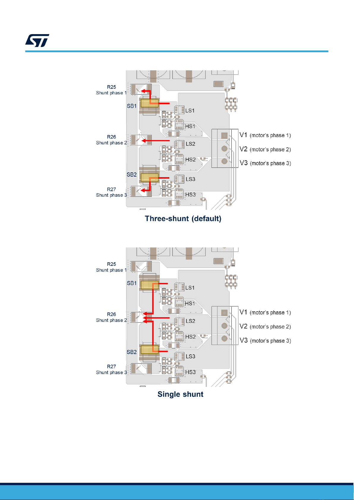
TP6 PH_1 Voltage of the phase V1 (U) of the motor, rescaled and filtered.
TP7 PH_2 Voltage of the phase V2 (V) of the motor, rescaled and filtered.
TP8 PH_3 Voltage of the phase V3 (W) of the motor, rescaled and filtered.
TP9 I1 Amplified signal related to the current flowing in the phase V1 of the motor.
TP10 OPREF Reference voltage provided to the operational amplifiers.
TP11 I2 Amplified signal related to the current flowing in the phase V2 of the motor.
TP12 CFBK Amplified signal used by the comparator implementing the current control (Comparator for current control).
TP13 I3 Amplified signal related to the current flowing in the phase V3 of the motor.
TP14 CREF Reference signal used to set the current threshold of the current control (Comparator for current control).
UM3193
Hardware description and configuration
UM3193 - Rev 1 page 3/33

Ref. Label Description
TP15 5V 5 V output of the DC/DC Buck converter. 5 V supply is used to supply the control board connected to the MC
connector V2.
TP16 GND Signal ground, reference for the DC/DC and the MC connector V2. The control board is referred to this GND.
TP17 PG Power good indicator of the DC/DC Buck converter.
TP18 VM Voltage supply of the motor and the STDRIVE101. TP2 is placed next to the main power connector J7.
TP19 VBUS Bus voltage VM rescaled and filtered.
TP20 GND Power GND. Close to the main power connector J7.
TP21 TPCB Temperature signal measured by the NTC resistor.
1.1 MC connector V2
The Motor Control connector V2 is used to connect a compatible control board to the STEVAL-LVLP01. The
insertion slot of this 164-pin edge-card connector presents two rows of contacts: the row on the bottom has an
“A”, and the row on top has a “B” (see Figure 3) at the beginning and the end of the pin numbering sequence.
The signal mapping is reported in Table 4, which indicates:
• The category of the pin according to the functional block associated
• The direction of the signal, whether from the power board STEVAL-LVLP01 to the control board (P → C) or
vice-versa (P → C)
• The description of the signal function
The pins of the connector not reported in Table 4 can be associated to other functions or signals present on the
control board, but are unused by the STEVAL-LVLP01.
Figure 3. MC connector V2 footprint and pin numbering (top view)
UM3193
MC connector V2
UM3193 - Rev 1 page 4/33

Table 4. Pin mapping of the MC connector V2
Pin No. Category Direction Signal Name Description
A01
SPI
C → P SPI_nSS nSS signal generated by the SPI peripheral (Master) on the control board.
B01 P → C SPI_MISO MISO signal generated by the slave device connected to J11 on the STEVAL-LVLP01.
A02 C → P SPI_SCK Serial clock signal generated by the SPI peripheral (Master) on the control board.
B02 C → P SPI_MOSI MOSI signal generated by the SPI peripheral (Master) on the control board.
A05
Power
P → C 5V + 5V Supply voltage generated by the DC/DC converter on the STEVAL-LVLP01
B05
A06 C → P VDD +3.3V Supply voltage generated on the control board.
B06 -- VREF+ Reference voltage for the analog circuitry
A07 -- GND Reference GND
B07
A08 Board ID C → P ID ENABLE
Selects the analog signal to be sent on TEMP/ID pin (A28):
Set to 0: board ID
Set to 1: temperature sensor
B08 Power -- GND Reference GND
A12
Motor Feedback P → C nFAULT
STDRIVE101 fault indicator (active low): connection to BKIN input of the timer.
B12 STDRIVE101 fault indicator (active low): connection to BKIN2 input of the timer
(default).
A13
Motor control
C → P INH1 INH1/IN1 control Signal for the half bridge 1 (see Working mode selection).
B13 C → P INL1 INL1/EN1 control Signal for the half bridge 1 (see Working mode selection).
A14 C → P INH2 INH2/IN2 control Signal for the half bridge 2 (see Working mode selection).
B14 C → P INL2 INL2/EN2 control Signal for the half bridge 2 (see Working mode selection).
A15 C → P INH3 INH3/IN3 control Signal for the half bridge 3 (see Working mode selection).
B15 C → P INL3 INL3/EN3 control Signal for the half bridge 3 (see Working mode selection).
B16
Motor Feedback
P → C ENCA A+ signal from the motor digital encoder
A17 P → C ETR ETR signal from the current control comparator (see Comparator for current control).
B17 P → C ENCB B+ signal from the motor digital encoder
A18 P → C H1 Hall sensor 1 digital signal
B18 P → C ENCZ Zero feedback signal from the motor digital encoder
A19 P → C H2 Hall sensor 2 digital signal
B19 P → C H3 Hall sensor 3 digital signal
A20 Power -- GND Reference GND
B20
A21
Motor Feedback
P → C ISNS1P Current sensing signal (positive) related to motor’s phase 1 (U) (see Operational
amplifiers).
B21 P → C ISNS1N Current sensing signal (negative) related to motor’s phase 1 (U) (see Operational
amplifiers).
A22 P → C ISNS2P Current sensing signal (positive) related to motor’s phase 2 (V) (see Operational
amplifiers).
B22 P → C ISNS2N Current sensing signal (negative) related to motor’s phase 2 (V) (see Operational
amplifiers).
A23 P → C ISNS3P Current sensing signal (positive) related to motor’s phase 3 (W) (see Operational
amplifiers).
UM3193
MC connector V2
UM3193 - Rev 1 page 5/33

Pin No. Category Direction Signal Name Description
B23 Motor Feedback P → C ISNS3N Current sensing signal (negative) related to motor’s phase 3 (W) (see Operational
amplifiers).
A24 Power -- GND Reference GND
B24
A25
Motor Feedback
P → C VSNS1 Voltage of the motor’s phase 1 (U) rescaled and filtered.
B25 -- GND Reference GND
A26 P → C VSNS2 Voltage of the motor’s phase 2 (V) rescaled and filtered.
B26 -- GND Reference GND
A27 P → C VSNS3 Voltage of the motor’s phase 3 (W) rescaled and filtered.
B27 -- GND Reference GND
A28 P → C TEMP/ID Analog signal representing the board ID or the temperature (see Temperature sensor
and board ID).
B28 Motor control C → P CURR_REF Reference signal used to set the current control (see Comparator for current control).
A29 Motor Feedback P → C VBUS Power stage bus voltage (VM) rescaled and filtered
A31
Power -- GND Reference GND
B31
A32
B32
A45
B45
A49
B49
A56
B56
A65
B65
UM3193
MC connector V2
UM3193 - Rev 1 page 6/33

1.2 Getting started
Table 5 summarizes the maximum ratings of the STEVAL-LVLP01. To run the motor follows the points below:
Step 1. Plug a compatible control board in the MC Connector V2 (J12), programmed with the target firmware
Step 2. Connect a power supply (voltage between 6V and 45V) to J7, taking care to connect the positive pole
to VM pin and the negative one to GND pin (see Figure 2)
Step 3. Connect the three-phase brushless motor to J3 taking care of the motor phase sequence
Step 4. In case motor sensors are needed (disregard this point if the application does not require them):
Step 4a. Select which supply to use for the Hall sensors using J5 and connect the Hall sensors and
their supply to J6
Step 4b. Select which supply to use for the encoder using J8 and connect the encoder and its supply
to J9
Step 5. Power up the voltage supply connected to J7 and start the application.
Table 5. STEVAL-LVLP01 operative conditions
Parameter Value
Supply voltage Nominal From 6 V to 45 V
Maximum phase current Continuous(1) 5 Arms
Peak (OC protection enabled – J2 open) 20 Amax
1. Actual maximum current could be limited by power dissipation
UM3193
Getting started
UM3193 - Rev 1 page 7/33

2 Hardware and functional blocks description
The STEVAL-LVLP01 is based on the STDRIVE101 three-phase gate driver. The power stage is based on six N-
channel STL8N10F7 power MOSFETs in the 3.3 x 3.3 powerFLAT package. The digital control signals and the
feedback signals are routed on the MC connector V2, which acts as interface for the control board.
The STEVAL-LVLP01 can be configured in single-shunt or three-shunt and it can support FOC, six-step, ZeST,
and HSO algorithms. Each part of the Figure 4 block diagram is described in the following sections.
Figure 4. STEVAL-LVLP01 block diagram
2.1 DC-DC buck converter
The ST1S14 is a DC/DC buck converter present on the STEVAL-LVLP01, which generates a 5 V output, starting
from the motor supply VM provided on J7. The external components are sized in order to guarantee a maximum
current capability of 1.5 A. The 5 V voltage is brought on the MC connector V2, in order to provide the supply the
microcontroller present on the control board. The step down from 5 V to 3.3 V is usually done by a linear
regulator. The 5 V can also supply the motor sensors connected to the STEVAL-LVLP01 (see Motor position
feedback interfaces)
If needed, the extended current capability of the DC/DC allows the user to connect other external loads, in
addition to the other circuitries mentioned above. The 5 V voltage provided by the DC/DC is present on the test
point TP15; a “Power Good” signal present on TP17 indicates whether the 5V is ok or there are some issues in
regulation. Moreover, the “power good” is also indicated by the LED2 (green).
2.2 Current sensing
This section describes how the STEVAL-LVLP01 performs the current sensing, flowing in each phase of the
motor. The current sensing is a critical point because most of the motion control algorithms are based on this
information.
2.2.1 Shunt resistor configuration
The STEVAL-LVLP01 can be used in both three-shunt or single shunt configurations. By default, the board is
configured in three-shunt configuration. Every phase has a shunt resistor of 15 mΩ. It is possible to change from
three-shunt to single shunt, by changing the configuration of the solder bridges SB1 and SB2 as shown in
Figure 5 and Figure 6.
UM3193
Hardware and functional blocks description
UM3193 - Rev 1 page 8/33

Figure 5. Solder bridges configuration for three-shunt operation
Figure 6. Solder bridges configuration for single shunt operation
In case of single shunt operation (Figure 6) the solder bridges redirect the current of the three phases to flow in
the shunt resistor of the phase 2 (R26); the readout of the current must be performed on the ISNS2P and ISNS2N
signal; A22 and B22 pins of the MC connector V2, respectively.
UM3193
Current sensing
UM3193 - Rev 1 page 9/33

2.2.2 Operational amplifiers
By default, the shunt resistors are directly connected to the MC connector V2: the amplification can be done
exploiting the operational amplifiers embedded in the microcontroller on the control board. However, it is possible
to change this configuration and use the operational amplifiers present on the STEVAL-LVLP01. The signal of
each shunt resistor has a dedicated op-amp, which implements a differential amplifier with a gain of 15. The
topology used enables the rejection of the common mode, resulting in a more accurate output signal. There is the
possibility to add a RC low pass filter at the output of each op-amp; by default, no filter is mounted. The TSV994
mounted on the STEVAL-LVLP01 embeds the three operational amplifiers (one for each shunt), together with a
fourth op-amp used for current control (see Comparator for current control).
By configuring the 0-Ohm resistors/solder bridges as reported in Table 6, the raw signal coming from the shunt
resistor is amplified before sending it the MC connector V2.
Figure 7. Shunt and op-amp connections by solder bridges / 0-ohm resistors
Table 6. Configuration for the shunt resistors amplification
Shunt resistor Direct to MC conn. V2 (default) To op-amp and then to MC connector V2
R25 (Phase 1) R43, R54 mounted/closed
R46, R49 open
R43, R54 open
R46, R49 mounted/closed
R26 (Phase 2) R62, R71 mounted/closed
R65, R69 open
R62, R71 open
R65, R69 mounted/closed
R27 (Phase 3) R79, R88 mounted/closed
R83, R86 open
R79, R88 open
R83, R86 mounted/closed
UM3193
Current sensing
UM3193 - Rev 1 page 10/33

2.2.3 Comparator for current control
The current control feature is implemented using the ETR pin of the microcontroller: this pin acts directly on the
timer driving the gate drivers of the STDRIVE101. The ETR signal is triggered when the value of the current
reaches the selected threshold. For this purpose, the comparator TS3021 compares a signal proportional to the
current with a reference signal representing the current threshold.
As the current is measured on the shunt R26, a single shunt topology should be used (as explained in Shunt
resistor configuration). The current control is particularly suitable for six-step algorithms, where only positive
voltages are used for the control. The voltage on R26 is then amplified, filtered and provided on the positive input
of the comparator (CFBK on Test point TP12). The amplification is performed by the fourth op amp of the TSV994
(see Operational amplifiers), implementing a differential amplifier with a gain equal to 22. The CREF signal (Test
point TP14) is connected to the negative input of the comparator and set the threshold of the current control.
Therefore, the current of the power stage is controlled at the peak level Ictrl that is:
Ictrl =VCREF
22 ∙ Rsℎunt =VCREF
330Ω
The voltage on CREF (VCREF) can be generated directly by the control board or provided externally (see
Figure 8). The reference signal generated by the control board (CURR_REF) could be an analog signal or a PWM
signal with a duty cycle proportional to the target voltage. The low pass-filter (R81 and C31) filters the PWM,
providing a stable VCREF.
Figure 8. current threshold selector
2.3 Motor phase voltage
The voltage present on each motor’s phase is rescaled and filtered, so it can be monitored by the microcontroller
on the control board. The attenuation of the resistor divider is about 25.3, ensuring that even at the maximum
supply VM, the signals are within the operative range of the microcontroller’s inputs. The bandwidth of the low
pass filter is 518 Hz.
The signals related to the motor’s phase voltages are available on the test points TP6, TP7, TP8 and on the MC
connector V2 as listed here below:
• Motor’s phase 1 signal: VSNS1 on TP6 and MC connector V2 pin A25
• Motor’s phase 2 signal: VSNS2 on TP7 and MC connector V2 pin A26
• Motor’s phase 3 signal: VSNS3 on TP8 and MC connector V2 pin A27
2.4 Temperature sensor and board ID
The two analog signals related to the temperature monitoring and to the board ID are mapped on the same line
connected to the MC connector V2 (TEMP_ID). An analog multiplexer selects which signal is sent to the MC
connector V2, according to the digital line ID_ENALBLE set by the control board:
• ID_ENABLE = 0 → board ID signal on the MC connector V2
• ID_ENABLE = 1 → temperature signal on the MC connector V2
UM3193
Motor phase voltage
UM3193 - Rev 1 page 11/33

2.4.1 Board ID
The board ID provides a voltage level which identifies the STEVAL-LVLP01; this analog voltage is obtained with a
resistor divider referred to the VDD, which is 3.3 V typical and it is also the supply of the microcontroller on the
control board. The voltage level identifying the STEVAL-LVLP01 is approximately 1.03 V.
2.4.2 Temperature sensor
The temperature measurement is implemented using an NTC resistor placed on the STEVAL-LVLP01, between
the power MOSFETs and the output connector J3. A voltage proportional to the temperature is generated by the
resistor divider given by NTC1 and R109 and it is available on TP21.
The NTC resistance decreases when the temperature increases with a non-linear relation (Figure 9): it is not
possible to obtain a linear behavior on the entire temperature range. R109 is sized in order to get a linear
behavior in the most critical temperature range, between 50°C and 120°C (Figure 10). The relation to find the
temperature, only valid for temperatures between 50°C and 120°C is:
T°C= 45.7 ∙ VTP21 V+ 23.6
Figure 9. NTC resistance value with respect to temperature
Figure 10. Voltage on TP21 with respect to temperature
2.5 Motor position feedback interfaces
The STEVAL-LVLP01 embeds three different interfaces (Figure 11) to acquire the motor sensors and send them
through the MC connector V2 to the control board. These signals are then managed by the microcontroller to
implement the motion control algorithms.
UM3193
Motor position feedback interfaces
UM3193 - Rev 1 page 12/33

Figure 11. Strip connectors for motor sensor feedback
2.5.1 Hall sensor connector
The Hall sensor connector J6 supports digital Hall sensors with open drain output. The 4.7 kΩ pull-up resistors
(R96, R97, R98) connected to VDD shift the input signals to a level compatible with the microcontroller’s inputs
range. A low pass filter is also present to reduce the noise during transitions. Refer to Table 2 for the connector J6
pinout. The order of sensors’ outputs H1, H2 and H3 must be coherent with the related motor’s phases connected
to the output connector J3. The Hall sensors supply (“VHall” label) is provided on the pin 4 of the J6 connector:
both the 5 V and the 3.3 V supplies are supported and the selection is made by J5:
• Jumper between the pin 1 and pin 2: sensors powered by 5 V supply
• Jumper between the pin 2 and pin 3: sensors powered by 3.3 V supply (VDD)
2.5.2 Digital encoder connector
The encoder connector J9 supports a quadrature encoder with push-pull outputs. The encoder’s signals are
shifted to a level compatible with the microcontroller’s inputs range. Refer to Table 2 for the connector J9 pinout.
The encoder supply (“VEnc” label) is provided on pin 4 of the J9 connector: both the 5 V and the 3.3 V are
supported; the selection is made by J8:
• Jumper between the pin 1 and pin 2: sensors powered by 5 V supply
• Jumper between the pin 2 and pin 3: sensors powered by 3.3 V supply (VDD)
2.5.3 SPI connector
The Serial Peripheral Interface (SPI) is a general purpose interface and can be used to connect a generic digital
sensor supporting this interface (e.g. a digital absolute encoder). The SPI is mapped on J11; refer to Table 2 for
the connector’s pinout. The device connected to J11 can act only as slave in the communication. The SPI supply
(“VSPI” label) is provided on pin 5 of the J11 connector: both the 5 V and the 3.3 V are supported; the selection is
made by J10:
• Jumper between the pin 1 and pin 2: sensors powered by 5 V supply
• Jumper between the pin 2 and pin 3: sensors powered by 3.3 V supply (VDD)
2.6 Bus voltage monitoring
The bus voltage VM (HS MOSFETs supply) is rescaled and filtered, so it can be monitored by the microcontroller
on the control board. The attenuation of the resistor divider is about 25.3, ensuring that even at the maximum
supply VM, the signals are within the operative range of the microcontroller inputs. The bandwidth of the low pass
filter is 518 Hz. The signal related to the bus voltages is available on the test point TP19 and on the MC connector
V2 on the pin A29. The green LED3 indicates the presence of the supply VM.
UM3193
Bus voltage monitoring
UM3193 - Rev 1 page 13/33

3 STDRIVE101 feature descriptions
3.1 Overcurrent comparator
The STDRIVE101 integrates a comparator, which disables the power stage whenever the voltage on its input (CP
pin) exceed the internal threshold VREF,DRV (about 0.5V). The values of the currents in each phase are acquired
and combined through a resistors’ network: the resulting signal, connected to CP is proportional to the current .
The resistors R7, R8, R9 have the same value and act as a voltage adder, while the R6 introduces a shift on the
resulting signal. Defining a ratio α equal to:
α=R7
R6=R8
R6=R9
R6=2.2kΩ
5.1kΩ= 0.43
The current threshold which triggers the comparator is:
IOC =1
Rsℎunt ∙3VREF +αVREF − αVDD =1
15mΩ∙1.5V+ 0.215V − 1.42V ≈ 19.7A
The C7 capacitor filters the signal, which is directly modulated by the PWM switching of the power stage.
Therefore, there is a delay in the intervention time of the comparator.
The overcurrent comparator can be disabled shorting the CP pin to GND, closing strip J2 with a jumper.
3.2 VDS monitoring protection
The STDRIVE101 embeds a protection which measures the voltage between the drain and the source of each
MOSFET (VDS) and compares it with a specified threshold. When the MOSFET is turned on and its VDS is
greater than the threshold, the VDS monitoring protection is triggered after a deglitch time. The threshold is set on
the SCREF pin of the STDRIVE101 through the divider given by R1 and R4: it is approximately 0.88 V.
Note: The drop on the LS MOSFETs is measured between their drain and GND, so the drop on the respective shunt
resistor contributes to the measurement. For further information, refer to STDRIVE101 datasheet.
The VDS monitoring protection can be disabled closing with a jumper the pins of J1.
3.3 Embedded 12 V linear regulator
The STDRIVE101 embeds a linear regulator which supplies the gate drivers. The voltage generated by the linear
regulator is available on the REG12 pin connected to the test point TP1.
3.4 Working mode selection
The STDRIVE101 has two input strategies, which can be selected by changing the resistor R5 connected to the
DT/MODE pin of the device. The default value of R5 is 0 Ω (short to GND), meaning that the STDRIVE101 works
in direct mode: the status of each driver is determined by the status of its related input signal: INHx for the high-
side MOSFET and INLx for the low-side MOSFET, with x = 1,2 or 3.
Changing the value of R5 with a resistor in the range between 50 kΩ and 250 kΩ, the STDRIVE101 works in
enable/input mode: the half bridge “x” is enabled or disabled by ENx signal and its status is determined by INx
signal. The deadtime between the HS and LS switching depends on the value of the R5 resistor. Table 7
summarizes the function of each digital input according to the configuration. For further information, refer to the
STDRIVE101 datasheet.
Table 7. STDRIVE101 digital input functions according to R5 (DT/MODE pin)
STDRIVE101 Pin name
(number)
Direct Mode
(R5 = 0 Ω)
EN/IN Mode
(50kΩ < R5 < 250 kΩ)
INH1/IN1 (7) INH1 (digital control input for the HS driver on
half bridge 1)
IN1 (level of half bridge 1: HS or LS on, with
deadtime insertion)
INH2/IN2 (8) INH2 (digital control input for the HS driver on
half bridge 2)
IN2 (level of half bridge 2: HS or LS on, with
deadtime insertion)
INH3/IN3 (9) INH3 (digital control input for the HS driver on
half bridge 3)
IN3 (level of half bridge 3: HS or LS on, with
deadtime insertion)
INL1/EN1 (10) INL1 (digital control input for the LS driver on
half bridge 1)
EN1 (digital control of the half bridge 1: enable/high
impedance)
UM3193
STDRIVE101 feature descriptions
UM3193 - Rev 1 page 14/33

STDRIVE101 Pin name
(number)
Direct Mode
(R5 = 0 Ω)
EN/IN Mode
(50kΩ < R5 < 250 kΩ)
INL2/EN2 (11) INL2 (digital control input for the LS driver on
half bridge 2)
EN2 (digital control of the half bridge 2: enable/high
impedance)
INL3/EN3 (12) INL3 (digital control input for the LS driver on
half bridge 3)
EN3 (digital control of the half bridge 3: enable/high
impedance)
3.5 Fault monitoring
When a protection of the STDRIVE101 is triggered (overcurrent, VDS monitoring, UVLO or overtemperature), the
internal open drain MOSFET of the nFAULT pin is turned on. A red LED (LED1) is present and it is activated and
the status can be read also on the test point TP3.
The nFAULT signal can be mapped on two different pins of the MC connector V2: by default it is mapped on B12:
in this case the nFAULT signal triggers the BKIN2 input of the timer peripheral in the microcontroller on the control
board. Mounting R117 and removing the R118 instead, the nFAULT pin will be redirected on A12 pin of the MC
connector V2, thus triggering the BKIN input of the timer peripheral.
UM3193
Fault monitoring
UM3193 - Rev 1 page 15/33

4 Schematic diagrams
Figure 12. STEVAL-LVLP01 circuit schematic (1 of 6)
VM
nFAULT
FAULT
MODE/DT
REG12
Closed: Vds monitoring protection disabled
Open (default): Vds monitoring protection enabled
SCREF
CP
Closed: OC comparator protection disabled
Open (default): OC comparator protection enabled
Gate Driver STDRIVE101
STDRIVE101 comparator network
STDRIVE101 VDS monitoring threshold
CP _ drv
CP _ drv
SCR EF
SCREF
12V VM
VDD
VDD
VDD
VDD
INH1
INH2
INH3
INL1
INL2
INL3
nFAULT
GLS1
OUT1
GHS 1
GLS2
OUT2
GHS 2
GHS 3
GLS3
OUT3
SHUNT1P
SHUNT2P
SHUNT3P
OUT1
OUT2
OUT3
TP2
R1
33k
1%
JP 2
GND_no de
1 2
R9 2.2k 1%
R3
39k
C8
1uF
25V
U1
STDRIVE101
BOOT1 21
BOOT2
17
BOOT3
13
CP 1
DT_MODE 2
GHS 1 22
GHS 2
18
GHS 3
14
GLS1 24
GLS2 20
GLS3
16
Epa d/GND
25
INH1_IN1
7
INH2_IN2
8
INH3_IN3
9
INL1_EN1
10
INL2_EN2
11
INL3_EN3
12
OUT1 23
OUT2 19
OUT3
15 REG 12 5
SCR EF 3
VS 4
nFAULT 6
TP4
TP1
R5 0
C9
1uF
25V
C2
220nF
25V
C6
1uF
25V
JP 1
GND_no de
1 2
C7
3.3nF
C3
100nF
100V
R2
470
R4
12k
1%
J1
1
2
TP3
LED1
RED
1 2
J2
1
2
R7 2.2k 1%
C4
1uF
100V
C5
10nF
C1
22uF
25V
R6
5.1k
1%
R8 2.2k 1%
UM3193 - Rev 1 page 16/33
UM3193
Schematic diagrams

Figure 13. STEVAL-LVLP01 circuit schematic (2 of 6)
1
2
3
PH_1 PH_2
PCI-e connector sideMotor connector side PCI-e connector sideMotor connector side
PH_3
PCI-e connector sideMotor connector side
GND
default:
close 1-2
for 3-shunt
configuration
default:
close 2-3
for 3-shunt
configuration
LSS 1
LSS 2
LSS 3
V3
V1 V2 V3
V1
V2
VM VM VM
GHS 1
OUT1
GLS1
GHS 2
OUT2
GLS2
GHS 3
GLS3
OUT3
SHUNT1P
SHUNT1N
SHUNT2P
SHUNT2N SHUNT3N
SHUNT3P
VSNS 1 VSNS 2 VSNS 3
D1BAT30K
R20 100
C17
NM
12
R14 39
Q2
STL8N10F7
1
4
5
2 3
6 7 8
R34
NM
R30
68k
1%
D3BAT30K
TP6
D4BAT30K
R39
3.9k
1%
C11
220nF
100V
TP5
R18 0
C10
220nF
100V
D6BAT30K
R11 100
R13 39
R16 0
R29
27k
1%
R31
27k
1%
12
R28
68k
1%
TP8
R36
NM
D5BAT30K
SB1
11
2
23
3
R15 39
R32
68k
1%
Q4
STL8N10F7
1
4
5
2 3
6 7 8
Q6
STL8N10F7
1
4
5
2 3
6 7 8
C14
82nF
R10 100
R35
3.9k
1%
R38
NM
R24 39
R17 0
C13
82nF
C16
NM
R19 100
R37
3.9k
1%
Q3
STL8N10F7
1
4
5
2 3
6 7 8
R12 100
Q1
STL8N10F7
1
4
5
2 3
6 7 8
SB2
11
2
23
3
D2BAT30K
R33
27k
1%
12
R23 39
C12
220nF
100V
J3
MORS V-508-3P_screw
1
2
3
R22 39
R26
15m
1W
1%
C18
NM
R21 100
TP7
R25
15m
1W
1% R27
15m
1W
1%
Q5
STL8N10F7
1
4
5
2 3
6 7 8
C15
82nF
UM3193 - Rev 1 page 17/33
UM3193
Schematic diagrams

Figure 14. STEVAL-LVLP01 circuit schematic (3 of 6)
OPREF
I1
CREF
CFBK
I3
I2
CURR_REF_IN
GND
SBR
SBR
SBR
SBR
SBR
SBR
SBR
SBR
SBR
SBR
SBR
SBR
SBR
SBR
SBR SBR
SBR
Phase Current sensing
Comparator for current control
Voltage reference generation
100 nF 10 k
10 k
TS461CLT
1 nF
10 k
100
CFBK
CFBK
OP REF
VDD
OP REF
VDD
VDD
VDD_f
VDD_f VDD_c VDD
VDD_c
OPREF
OP REF
VREF+
SHUNT1P
SHUNT1N
SHUNT2P
SHUNT2N
SHUNT3P
SHUNT3N
CURR_REF
ETR
SHUNT2P
SHUNT2N
SHUNT1P
SHUNT1N
ISNS 1N
ISNS 1P
SHUNT3P
ISNS 3P
SHUNT2N
SHUNT3N
ISNS 2N
ISNS 3N
ISNS 2P
SHUNT2P
R60 NM
+
-
U2B
TSV994AIPT
IN+5
IN-6
OUT 7
R73 1k
TP11
R54 0
R61
30k
0.1%
R59
NM
C23
2.2u
C31
10nF
TP14
R84 1k
0.1%
R40 4.7
R79 0
R74 10k
R45 0
R50
NM
R63 1k
0.1%
R56 30k 0.1%
R42
30k
0.1%
J4
1
2
3
R75 1k
C26
1nF
R86 NM
C22
NM
R67 1k
0.1%
C32
NM
R69 NM
R87 30k 0.1%
U3
NM
1
OUT
V-
2
+
3
-
4
V+ 5
R68
30k
0.1%
R44 1k
0.1%
R83 NM
C29
47p
R58
NM
R88 0
TP10
R52 0
R71 0
TP13
C27
NM
R77 22k
R47 1k
0.1%
R82 0
R57
NM
TP12
C24
NM
R70 30k 0.1%
R62 0
+
-
U2C
TSV994AIPT
IN+10
IN-9
OUT 8
C25
NM
C28
100nF
R76
22k
C21
1nF
R46 NM
R41 4.7
R66
NM
R53 30k 0.1%
C19
100nF
R51
0
V+
+
-V-
U4
TS3021ILT
1
4
5
3
2
R81 10k
R72 30k 0.1%
R64 0
R55
NM
R43 0
C30
1nF
C20
100nF
R49 NMR48
30k
0.1%
R89 30k 0.1%
+
-
U2D
TSV994AIPT
IN+12
IN-13
OUT 14
R80 1k
0.1%
R65 NM
+
-
U2A
TSV994AIPT
Vcc-
11
IN+3
IN-2
OUT 1
Vcc+
4
R78
30k
0.1%
R85
30k
0.1%
TP9
UM3193 - Rev 1 page 18/33
UM3193
Schematic diagrams

Figure 15. STEVAL-LVLP01 circuit schematic (4 of 6)
5V
PG
SBR
SBR
Buck converter for 5V generation
GND_S
FB
P_GO OD
FB
P_GO OD
VM
5V
Buck_OUT
Buck_OUT
TP15
C36
1nF
Q7
BSS 1 23
3
1
2
C35
47u
16V
U5 ST1S 14PHR
BOOT
1
EN2 5
EP AD
9
FB
4
GND 6
PG
2
SW 8
VIN 7
EN1
3R93
4.7k
C33 100nF
100V
C37
100nF
100V
R92 0
LED2
GREEN
1 2
L1 10uH
C38
4.7uF
100V
TP17
R91
47k
D7
STP S 2L60
12
C34
47u
16V
TP16
R95
1.5k
R94
1k
R90
0
UM3193 - Rev 1 page 19/33
UM3193
Schematic diagrams

Figure 16. STEVAL-LVLP01 circuit schematic (5 of 6)
Hall sensors
supply:
default to 5V
GND
H1
H2
H3
VHall
Quadrature
encoder supply:
default to 5V
GND
A
B
Z
VEnc
SPI Encoder supply:
default to 5V
GND
MISO
MOSI
SCLK
VSPI
nSS
TPCB
+
-6V-45V
PCI-e connector sideSupply connector side
VBUS
Power supply connector (VM)
Board ID and temperature sensor (NTC)
Hall sensors connector
Quadrature Encoder connector
SPI connector
VM
GND
TPCB
VDD 5V
VDD
VDD 5V
VDD 5V
VDD
VDD
VDD
VMVM
VDD
VDD
H1
H2
H3
ENCA
ENCB
ENCZ
SP I_nSS
SP I_MISO
SP I_MOS I
SP I_S CK
TEMP_ID
VBUS
ID_ENABLE_n
C46
NM
C50
10nF
R104 3.3k
R111
10k
R96
4.7k
U7
STG3157CTR
S1
1
GND
2S2
3D4
VCC
5IN 6
J7
MORS V-508-2P_screw
2
1
R105
15k
C41
82 nF
J11 1
2
3
4
5
6
D9 BAT30K
R106 330
U6A
CD74HC4050
3 2
18
C44
2.2n
U6C CD74HC4050
7 6
TP18
C51
10nF
J6 1
2
3
4
5
C47
NM
U6F CD74HC4050
14 15
C43
2.2n
R114 100
C45
2.2n
R99
68k
1%
J5
1
2
3
D10 BAT30K
C42
330nF
25V
R107 330
NTC1
10k
12
TP21
C52
330nF
25V
C48
330nF
25V
R98
4.7k
R100
27k
1%
+
C39
47uF
100V
U6D CD74HC4050
9 10
C49
NM
R109
910
R101 3.3k
R113 100
R112 2 2k
R115 100
R108 330
TP20
R110
22k
J10
1
2
3
R97
4.7k
R103
3.9k
1%
J9 1
2
3
4
5
+
C40
47uF
100V
LED3
GREEN
1 2
R102 3.3k
U6B CD74HC4050
5 4
D8 BAT30K
R116 100
TP19
J8
1
2
3
U6E CD74HC4050
11 12
UM3193 - Rev 1 page 20/33
UM3193
Schematic diagrams
Table of contents
Other ST Motherboard manuals

ST
ST STM3210B-EVAL User manual

ST
ST STEVAL-MKI109V2 User manual

ST
ST STEVAL-IHM020V1 User manual

ST
ST STM3241G-EVAL User manual

ST
ST AN3954 Installation and operating instructions

ST
ST STEVAL-AETKT2V1 User manual

ST
ST SPC572LADPT100S User manual

ST
ST TN100 RF User manual

ST
ST STEVAL-ISB68WA User manual

ST
ST L9678-S-EVB User manual

ST
ST EVAL-L99MOD5xXP User manual

ST
ST EVAL-L99DZ200 User manual

ST
ST STEVAL-IDB007V Series User manual

ST
ST STM32L476ZG User manual

ST
ST STM32L5 Nucleo-144 board User manual

ST
ST ST9 Series User manual

ST
ST SPC5-UDESTK User manual

ST
ST SGS-Thomson ST624x-KIT Series User manual

ST
ST STR730-EVAL User manual

ST
ST STM32G4 Nucleo-64 User manual