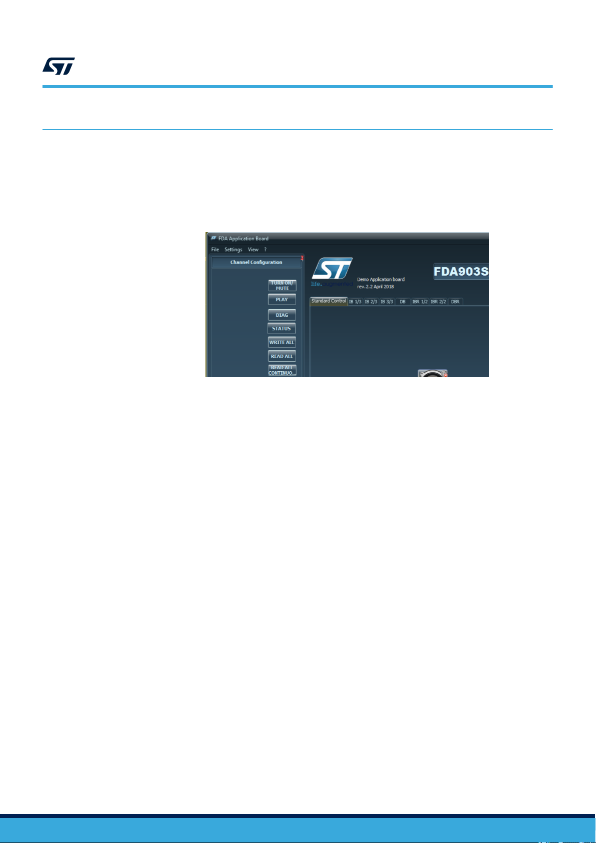
ST FDA803S User manual

Introduction
This document describes how to use the evaluation board in order to check FDA803S and FDA903S device’s performance.
For any other information and deeper details, refer to the FDA803S and FDA903S datasheets.
Evaluation board for FDA803S and FDA903S power amplifiers
UM2999
User manual
UM2999 - Rev 1 - March 2022
For further information contact your local STMicroelectronics sales office.
www.st.com

2General information
This evaluation board/kit is intended for use as ENGINEERING DEVELOPMENT, DEMONSTRATION, OR
EVALUATION PURPOSES ONLY and is not considered by ST Microelectronics to be a finished end-product
fit for general consumer use. People handling the product(s) must have electronics training and observe good
engineering practice standards.
This evaluation board/kit does not fall within the scope of the European Union directives regarding
electromagnetic compatibility, restricted substances (RoHS), recycling (WEEE), FCC, CE or UL, and therefore
is not requested to meet the technical requirements of these directives or other related directives.
UM2999
General information
UM2999 - Rev 1 page 3/21

3Board description
The board features a single channel Class-D amplifier able to deliver up to 10 W (14.4 V at 4 Ω), based on the
FDA903S (or FDA803S) and is intended to demonstrate the device capabilities.
Figure 1. Top view
Figure 2. Bottom view
UM2999
Board description
UM2999 - Rev 1 page 4/21

3.1 Board connection
The board can be connected directly to other ST modules such as the Extend Board Mini A2 and MiniA2 via
connector J10.
Figure 3. FDA903S Demo SA board + Extend board MiniA2 + Mini A2 board
To PC USB
Vbat
(optional)
R146
I2S ext.
Optical In
R12
R7
R13
(Bottom
side)
VCC
FDA903
Demo SA
Extender
board
MiniA2
Mini A2
J7, JP1-4 settings
required for audio
source selection
For information on the configuration and start-up procedures of the mentioned additional modules, dedicated
documentation is available (see Section 5 Quick start guide).
UM2999
Board connection
UM2999 - Rev 1 page 5/21

3.1.1 Connectors and connections
Power supply
The amplifier power supply (VCC) with a voltage value between 3.3 V and 18 V can be connected to the J5
terminal as shown by the markings on the board.
Outputs
The amplifier outputs are connected to the J1 terminals.
Board cascading
The bus expansion connectors J8-J9 make it possible to address and drive cascaded amplifier boards using the
same I2C control and I2S (TDM mode) signal lines.
3.2 Board options
Vbus voltage reference
An on-board voltage reference is used to supply the pull-up resistors connected to digital lines. In order to
measure the Vbus current consumption, J2 can be used.
Attention: Do not use J2 to connect an external voltage source.
Address selection
As described in the datasheet, it is possible to modify the I2C address of the device by suitably removing R7
or/and R6, and adding R15 or/and R16. However, no HW modification is required to set the I2C addresses if the
GUI is used through the Mini A2 board. The board is already configured to be used with the Mini A2 board (see
Section 5 Quick start guide).
HW Mute
The hardware muting/unmuting is controlled through the connector J10, in turn tied to the MUTE pin (J10 pin 31).
CD/Diag
The CD/DIAG function can be monitored through the J10 connector, in turn tied to the CD/DIAG1 and CD/DIAG2
pins (J10 pins 19 and 33).
Load current monitor (only for FDA903S)
The FDA903S is able to sense the current flowing through the load and communicate its value to the system host
micro.
Setting IB15[5] to ‘1’, the information is available to the host via I2C inside the read registers DB8 and DB9,
whereas setting IB2[2] to ‘1’, the real time information is available via I2S bus through the I2S_SDA2 data line.
UM2999
Board options
UM2999 - Rev 1 page 6/21

4Startup sequence
The following start-up procedure is recommended:
1. Connect J5 to a 14.4 V supply
2. Provide an I2S input signal (the device works as I2S slave, so the clock must be provided by the signal
source)
3. Load the device file (.dev) provided by ST
4. Load the default register setting file (.cfg), if available. If no .cfg file is available, the configuration set in
the .dev file is applied.
At the end of the sequence, the device is ready to transition to the desired operating status such as “play”.
UM2999
Startup sequence
UM2999 - Rev 1 page 7/21

5Quick start guide
This chapter describes a few steps to have audio output by the amplifier using the complementary ST tools:
Extend Board MiniA2, Mini A2 board and control Graphical User Interface.
5.1 Hardware connection
• Extend board MiniA2 (if present):
– It is recommended to supply the Extend board MiniA2 through the VCC supply rail of the FDA803S
Demo SA Board. In this case R12 (0 Ω) must be inserted.
As an alternative, the Extend board can be supplied by the Mini A2 board VBAT supply. In this case
R12 must be removed.
– Connect the Extend board MiniA2 to the Mini A2 board on one side and to the FDA803S DEMO SA
board on the other, as shown in Figure 3.
– Connect the desired audio source to the Extend board MiniA2 and set the jumpers (J7, JP1-4) to select
the correct input (refer to the Extend board MiniA2 manual for details).
– Since the Extend board MiniA2 has R7 mounted by default shorting I2S_SDA1 to I2S_SDA2, remove
R7 in case the FDA903S is mounted on the board and if the I2S_SDA2 is used independently to read
the current sensing values.
• MINI A2 Board:
– Connect the USB port connector J5 (near the corner) to a PC USB port.
– In case the alternative supply concept is used of the Extend Board miniA2 (R12 not mounted), check
that the resistor R146 is present and the VBAT connector is connected to a power supply (min 5 V, max
25 V) (by default R146 is not mounted).
• FDA803S Demo SA Board:
– Connect the VCC power supply (J5) and the load (J1).
– Make sure that R13 (0 Ω) is mounted to supply the Extend board as recommended (by default R13 is
not mounted).
Attention: It is not allowed to supply the VCC power line of the FDA803S Demo SA from the MiniA2 connector (VBAT)
side.Consequently, the 3 resistors (R12, R13, R146) must not all be mounted at same time.
UM2999
Quick start guide
UM2999 - Rev 1 page 8/21

6GUI setup
• Unzip the device file (“Mini A2 FDA803S-*.zip” or “Mini A2 FDA903S-*.zip”) in the GUI installation
folder “.\AccordoGUIFDAXXX\Devices\”. It includes the amplifier’s specific registers description
(FDA803S.dev or FDA903S.dev) and if available, the configuration file (registers best settings,
FDAx03S_I2Cbest_Setting.cfg).
• Launch the GUI (rev 2.2 april 2018) with the Mini A2 board connected to the PC via USB(J5). When the
module is detected, two “LED’s” on the bottom left of the GUI panel start blinking:
– Menu “Settings” → ”serial port”: select the proper COM port;
–Menu “Settings” → ”I2C Setup”: configure the proper I2C address by clicking the button “Find Device
Address”;
Figure 4. I2C setup
– Menu “File” → ”Open Device File”: select the FDA903S.dev or FDA803S.dev file present in the
“.\AccordoGUIFDAXXX\Devices\” folder;
– Menu “File” → ” Open Reg Values File”: select the FDAx03S_I2Cbest_Setting.cfg file if present in the
“.\AccordoGUIFDAXXX\Devices\” folder.
Attention: If at any time a pop-up window appears with a “read violation“ notification, it must be ignored. Operation can
continue normally after discarding the pop-up.
UM2999
GUI setup
UM2999 - Rev 1 page 9/21

7Device setup for playback
• Turn the device on with an I2S clock present:
– Click the buttons “channel conf.” followed by “Write all“ to apply the settings loaded from the
“FDAx03S_I2Cbest_Setting.cfg” file;
– Click the “PLAY” button.
Figure 5. Channel configuration
UM2999
Device setup for playback
UM2999 - Rev 1 page 10/21

8Board schematic
The Figure 6 shows the schematics of the “6038-506.20 v1.0 FDA803S DEMO SA“ board.
Figure 6. 6038-506.20 v1.0 FDA803S DEMO SA schematic
I2C_SCL
I2S_SCL
I2S_WS
I2C_SDA
C7
4.7uF
C6
10nF
1
F1
1
F2
1
F3
1
F4
EN1
EN2
CH1+
CH1-
SPEAKER CONNECTOR
J1
I2S_SCL
I2S_WS
I2S_SDA1
I2S_SDA2
2
4
6
8
10
1
3
5
7
9
11 12
13 14
15 16
17 18
19 20
21 22
23 24
25 26
27 28
29 30
31 32
33 34
35 36
37 38
39 40
J10
20x2 p2.54mm M Horiz.
CD/DIAG1
I2C_SCL
Vbatt
I2C_SDA
HWMUTE
C5
100pF
VCCP
VCCN
GND_PWR
AVdd
DVdd
EN1
EN2
HWMUTE
TP5
OUT1+
TP8
OUT1-
I2S_SDA1
R4 0R
R3 0R
R2 0R
Le GND (fila con nr. pari) DEVE STARE IIN BASSO SUL PCB !!
I2S_SDA2
CH1-
CH1+
R13 0R NM
I2S_SCL
I2S_WS
I2S_SDA1
I2S_SDA2
NC
GNDI2C_SCL
I2C_SDA
GND
CD/DIAG
VBAT
EN1
EN2
EN3
EN4
HWMUTE
GPIO1
GPIO2
GPIO3
GPIO4
GPIO2
GPIO3
GPIO4
R1 0R
CD/DIAG2
R6
10K
Vbus
PCB NOTE:Place all thes e comp one nts nea r J10 connector
MINI A2 STD CONNECTOR
1-
3-
5-
39-
37-
35-
J10 silkscreen
...-
...-
CD/DIAG1
CD/DIAG2
C12
1uF
R5
10K
R14 0R
OUT1+
22
VCC1+
23
VCC1+
24
GND1+
21
GND1-
20
VCC1-
17
VCC1-
18
OUT1-
19
NC
3
DVdd 30
SGnd4
32
Enable1
27
Enable2
26
CD/Diag1 11
D1V8SVR 2
DGSVR 1
I2Cdata 6
I2Cclk 5
I2SdataOUT 7
I2SdataIN 8
I2Sclk 9
I2Sws 10
SGnd1
13
AVdd 16
A5VSVR 15
AGSVR 14
HWMute 4
UR5T
NC 31
NC
29
SGnd3
28
CD/Diag2 12
SGnd2
25
SLUG 33
U1
FDA903S
TP4
CH1+
TP7
CH1-
GND_DIG
GND_PWR
GND_SHLD
GND_ANA
TP9
GND
D2
BZT52C2V7T-7
Vbus
POWER SUPPLY BLOCK
11
2
233
4
455
6
677
8
899
10
10 11 11
12
12 13 13
14
14 15 15
16
16
J8
8x2 p2.54mm M Horiz.
I2C_SCL
I2C_SDA
11
2
233
4
455
6
677
8
899
10
10 11 11
12
12 13 13
14
14 15 15
16
16
J9
8x2 p2.54mm F Horiz.
BUSES EXP CONNECTORS
C25
1uF
C24
100nF
VCCP
C34
1uF
C33
100nF
C29
33nF
C30
33pF
C28
470uF
4.7uH
L3
D1
SM6T22CAY
C26
4.7uF
C19
100pF
C20
10nF
C22
100pF
C21
10nF
VCCN
Vbatt
AVdd
BLM2
BLM18BD102SN1
DVdd
CLOS E TO AVDD PINS
CLOS E TO DVDD PINS
CLOS E TO VCCP
J5
TP1
VCC
TP2
GND
2.7V VBUS GENERATION
I2C_SCL
I2C_SDA
I2S_SCLconn
I2S_WSconn
I2S_SDA1conn
I2S_SDA2conn
I2S_SCLconn
I2S_WSconn
I2S_SDA1conn
I2S_SDA2conn
10uHL2
C32
10nF
C23
10nF
BLM1
BLM18BA220SN1
I2S_SCLconn
I2S_WSconn
I2S_SDA1conn
I2S_SDA2conn
R7
10K
R8
10K
R9
10K
R15
10K nm
R16
10K nm
R17
10K nm
TP6
CD/DIAG2
TP3
CD/DIAG1
C1
TBDNM
C2
TBDNM
C3
TBDNM
C4
TBDNM
C8
TBDNM
C9
TBDNM
C10
TBDNM
C11
TBDNM
R10
4K7 NM
R12
4K7 NM
C13
100pF
C18
100pF
C17
100pF
C31
100pF
C14
10nF
C15
4.7uF
C16
1uF
CLOS E TO VC CN
C27
470uF NM
1
F5
1
F6
10uHL1
J2
R18
2.2K
Vbatt
R20 0R NM
R11 0R NM
R19 0R
UM2999
Board schematic
UM2999 - Rev 1 page 11/21

9Bill of materials
The list provided here shows all the components (including parts necessary for this board but not required when
the IC is used in a real project) used to assemble the board described in this manual, with which performance
measurements have been performed. The manufacturer and part number information is provided to allow the user
to look up the characteristics of the components and select equivalent components from different manufacturers if
needed.
Table 2. Bill of materials
Qty Designator Description Value Tol. (1) (2) (3) (4) Package Manufacturer PN
1 BLM1
SMD EMI
Suppression
Filter
22 R 25% - 0.5 A - 100 0603 BLM18BA220SN1
1 BLM2
SMD EMI
Suppression
Filter
1 K 25% - 0.1 A - 100 0603 BLM18BD102SN1
5
C5, C13,
C17, C18,
C31
SMD MLCC
C0G/NP0
Capacitor
100 pF 5% 25 V - - - 0603 C0603X101J3GACAUTO
2 C6, C14 SMD MLCC
X7R Capacitor 10 nF 10% 25 V - - - 0603 C0603S103K3RACAUTO
2 C7, C15 SMD MLCC
X7R Capacitor 4.7 μF 10% 25 V - - - 0805 CGA4J1X7R1E475K125AC
2 C12, C16 SMD MLCC
X7R Capacitor 1 μF 10% 50 V - - - 1206 CGA5L3X7R1H105M160AB
2 C19, C22
SMD MLCC
C0G/NP0
Capacitor
100 pF 5% 50 V - - - 0603 CGA3E2NP01H101J080AA
4C20, C21,
C23, C32
SMD MLCC
X7R Capacitor 10 nF 10% 50 V - - - 0603 C0603X103K5RAC3316
2 C24, C33 SMD MLCC
X7R Capacitor 100 nF 10% 50 V - - - 0603 CGA3E2X7R1H104K080AA
2 C25, C34 SMD MLCC
X7R Capacitor 1 μF 10% 50 V - - - 0805 GCM21BR71H105KA03L
1 C26 SMD MLCC
X7R Capacitor 4.7 μF 10% 50 V - - - 1206 CGA5L3X7R1H475K160AB
1 C28 SMD Electrolytic
Capacitor 470 μF - 25 V - - - d10h10.2 EEEHA1E471P
1 C29 SMD MLCC
X7R Capacitor 33 μF 10% 50 V - - - 0603 C0603C333K5RACAUTO
1 C30
SMD MLCC
C0G/NP0
Capacitor
33 pF 5% 50 V - - - 0603 C0603C330J5GACAUTO
1 D1 Bidirectional 22
V Transil - - 22 V - 600 W - DO-214AA SM6T36CAY
1 D2 SMD 2.7V
Zener Diode - 7% 2.7 V - 0.3 W - SOD-523 BZT52C2V7T-7
2 J1, J5
TH Terminal
Header, Male, 2
position, p5.08
mm
- - - - - - p5.08mm 2008004
UM2999
Bill of materials
UM2999 - Rev 1 page 12/21

Qty Designator Description Value Tol. (1) (2) (3) (4) Package Manufacturer PN
1 J2
Header, 2-Pin,
Single row, TH,
Straight, Male
- - - - - - p2.54mm
1 J8
Header, 8-Pin,
Dual row, TH,
Right Angle,
Male
- - - - - - p2.54mm TSW-108-11-G-D-RA
1 J9
Header, 8-Pin,
Dual row, TH,
Right Angle,
Female
- - - - - - p2.54mm 803-87-016-20-001101
1 J10
TH Header
Male, Dual row,
20x2, p2.54
mm, Horiz.
- - - - - - p2.54mm TSW-120-08-L-D-RA
2 L1, L2 SMD inductor 10uH 20% - 1.6 A - - CUSTOM VCTA32251B-100MS6-11
1 L3 SMD inductor 4.7 μH 20% - 8.2 A - - CUSTOM IHLP-2020CZ-4R7M-A1
5R1, R2, R3,
R4, R14
SMD chip
resistor 0 Ω 1% 75 V - 0.1 W - 0603 CRCW06030000Z0EB
5R5, R6, R7,
R8, R9
SMD chip
resistor 10 KΩ 1% 75 V - 0.1 W - 0603 CRCW060310K0FKEB
1 R18 SMD chip
resistor 2.2 KΩ 1% 150 V - 0.125 W - 0805 CRCW08052K20FKEA
5
TP1, TP2,
TP3, TP6,
TP9
TH Test Point
terminal
Assembly - 1.04
mm
- - - - - - 20-2137
1 U1
1x10 W Class D
digital input
amplifier
- - 18 V - 45 W - QFN32 FDA903S / FDA803S
UNMOUNTED COMPONENTS
8
C1, C2, C3,
C4, C8, C9,
C10, C11
SMD Capacitor TBD - - - - - 0603
1 C27 SMD Electrolytic
Capacitor 470 μF - 25 V - - - d10h10.2 EEEHA1E471P
2 R10, R12 Surface mount
chip resistor 4.7 KΩ 1% 75 V - 0.1 W - 0603 CRCW06034K70FKEA
1 R13 SMD chip
resistor 0 Ω 1% 75 V - 0.1 W - 0603 CRCW06030000Z0EB
3R15, R16,
R17
SMD chip
resistor 10 KΩ 1% 75 V - 0.1 W - 0603 CRCW060310K0FKEB
1. Voltage rating
2. Current rating
3. Power rating
4. Frequency rating (in MHz)
UM2999
Bill of materials
UM2999 - Rev 1 page 13/21

10 Board layout
Figure 7. Assembly Top
Figure 8. Top layer
UM2999
Board layout
UM2999 - Rev 1 page 14/21

Figure 9. Layer 2
Figure 10. Layer 3
UM2999
Board layout
UM2999 - Rev 1 page 15/21

Figure 11. Bottom layer
Figure 12. Assembly Bottom
UM2999
Board layout
UM2999 - Rev 1 page 16/21

Revision history
Table 3. Document revision history
Date Version Changes
22-Mar-2022 1 Initial release.
UM2999
UM2999 - Rev 1 page 17/21

Contents
1Ordering information ..............................................................2
2General information ...............................................................3
3Board description .................................................................4
3.1 Board connection ..............................................................5
3.1.1 Connectors and connections................................................6
3.2 Board options..................................................................6
4Startup sequence..................................................................7
5Quick start guide ..................................................................8
5.1 Hardware connection ...........................................................8
6GUI setup..........................................................................9
7Device setup for playback ........................................................10
8Board schematic .................................................................11
9Bill of materials...................................................................12
10 Board layout......................................................................14
Revision history .......................................................................17
UM2999
Contents
UM2999 - Rev 1 page 18/21

List of tables
Table 1. Ordering information..................................................................2
Table 2. Bill of materials .................................................................... 12
Table 3. Document revision history ............................................................. 17
UM2999
List of tables
UM2999 - Rev 1 page 19/21

List of figures
Figure 1. Top view ........................................................................4
Figure 2. Bottom view ......................................................................4
Figure 3. FDA903S Demo SA board + Extend board MiniA2 + Mini A2 board ................................5
Figure 4. I2C setup ........................................................................9
Figure 5. Channel configuration .............................................................. 10
Figure 6. 6038-506.20 v1.0 FDA803S DEMO SA schematic .......................................... 11
Figure 7. Assembly Top.................................................................... 14
Figure 8. Top layer ....................................................................... 14
Figure 9. Layer 2 ........................................................................ 15
Figure 10. Layer 3 ........................................................................ 15
Figure 11. Bottom layer..................................................................... 16
Figure 12. Assembly Bottom ................................................................. 16
UM2999
List of figures
UM2999 - Rev 1 page 20/21
This manual suits for next models
1
Table of contents
Other ST Motherboard manuals

ST
ST STM32 Nucleo User manual

ST
ST STM8T141-EVAL User manual

ST
ST STM32L1 Series Installation and operating instructions

ST
ST STM32 Nucleo-64-P Series User manual

ST
ST STEVAL-L99615C User manual

ST
ST STEVAL-ISB042V1 User manual

ST
ST STEVAL-IDB007V Series User manual

ST
ST UM2313 User manual

ST
ST STM32CubeF4 User manual

ST
ST SPC572LADPT80S User manual

ST
ST STM32 Nucleo-32 User manual

ST
ST B-L4S5I-IOT01A User manual

ST
ST STEVAL-STRKT01 Administrator Guide

ST
ST NUCLEO-H745ZI-Q User manual

ST
ST STEVAL-ISW001V1 User manual

ST
ST STM32L4R9I User manual

ST
ST EVAL-L99H02XP User manual

ST
ST NUCLEO-F207ZG User manual

ST
ST UM2163 User manual

ST
ST ST25RU3993 User manual