ST SPC58XXMB User manual

Introduction
This document describes the STMicroelectronics SPC58XXMB evaluation board.
Figure 1. SPC58XXMB
SPC58XXMB evaluation board
UM2740
User manual
UM2740 - Rev 1 - January 2021
For further information contact your local STMicroelectronics sales office.
www.st.com

1Overview
This user’s manual details the setup and configuration of the STMicroelectronics SPC58XXMB evaluation
board (hereafter referred to as the EVB). The EVB is intended to provide a mechanism for easy customer
evaluation of the SPC58xx family and SPC57xx family of microcontrollers, and to facilitate hardware and software
development.
At the time of writing this document, the SPC58xx family will consist of the 40 nm powertrain and safety devices
and SPC57xx family will consist of the 55 nm powertrain and safety devices.
The EVB is intended for bench / laboratory use and has been designed using normal temperature specified
components (+70°C).
1.1 Package contents
An SPC58XXMB evaluation board package includes the following items:
• SPC58XXMB evaluation board
• Power supply 12 VDC – 2 A
• EULA
UM2740
Overview
UM2740 - Rev 1 page 2/45

2License agreement
The packaging of this evaluation board was sealed with a seal stating, " by breaking this seal, you agree to the
terms and conditions of the evaluation board license agreement, the terms and conditions of which are available
at https://www.st.com/resource/en/evaluation_board_terms_of_use/evaluationproductlicenseagreement.pdf ".
Upon breaking the seal, you and STMicroelectronics entered into the evaluation board license agreement, a
copy of which is also enclosed with the evaluation board for convenience.
Attention: This evaluation board only offers limited features for evaluating ST products. It has not been tested for use
with other products and is not suitable for any safety or other commercial or consumer application. This
evaluation board is otherwise provided “AS IS” and STMicroelectronics disclaims all warranties, express or
implied, including the implied warranties of merchantability and fitness for a particular purpose.
UM2740
License agreement
UM2740 - Rev 1 page 3/45

3Handling precautions
Please take care to handle the package contents in a manner such as to prevent electrostatic discharge.
Before the EVB is used or power is applied, please fully read the following sections on how to correctly configure
the board. Failure to correctly configure the board may cause irreparable component, MCU or EVB damage.
UM2740
Handling precautions
UM2740 - Rev 1 page 4/45

4Hardware description
4.1 List of acronyms
The table below provides a list and description of acronyms used throughout this document.
Table 1. List of acronyms
Acronym Description
1.25V_SR Supply voltage from the 1.25 V switching regulator
3.3V_SR Supply voltage from the 3.3 V switching regulator
5V_LR Supply voltage from the 5.0 V linear regulator
5V_SR Supply voltage from the 5.0 V switching regulator
ADC Analog-to-Digital converter
ESR0 External signal reset
EVB Evaluation board
FEC Fast ethernet controller module
GND Ground
HV High voltage (3.3 V and/or 5 V)
LED Light emitting diode
LV Low voltage (1.25 V)
MCU Microcontroller
OSC Oscillator
P12V 12 V EVB supply power domain
PORST Power-on reset
PWR Power
RX Receive
SIPI Serial Interprocessor Interface
TBD To be defined
TX Transmit
VSS Ground
UM2740
Hardware description
UM2740 - Rev 1 page 5/45

4.2 Modular concept
For maximum flexibility and simplicity, the EVB has been designed as a modular development platform. The EVB
main board does not contain an MCU. Instead, the MCU is fitted to an MCU daughter card (occasionally referred
to as an adapter board). This approach means that the same EVB platform can be used for multiple packages
and MCU derivatives within the SPC58xx family and the SPC57xx family. High density connectors provide the
interface between the EVB and MCU daughter cards as shown in the figure below. See Section 4.3 Daughter
card availability for more details on the daughter cards and Section 4.17 Board interface connectors for more
details on the interface connectors.
Figure 2. Modular concept - motherboard and MCU daughter card
For details on your specific daughter card, please consult the instructions included with the daughter card.
The EVB is designed to use the motherboard and the daughter in conjunction. However, it is possible to use the
daughter cards standalone.
UM2740
Modular concept
UM2740 - Rev 1 page 6/45

4.3 Daughter card availability
Table 2. Daughter card
Daughter card number Device
SPC58NHADPT176S SPC58NHxxE7
SPC58NHADPT302S SPC58NHxxC3
SPC58NHADPT386S SPC58NHxxC5
SPC58XCADPT176S SPC584BxxE7
SPC58xCxxE7
SPC58XCADPT292S SPC584CxxC5
SPC58XXADPT64S
SPC582BxxE1
SPC584BxxE1
SPC58xCxxE1
SPC58XXADPT100S
SPC582BxxE3
SPC584BxxE3
SPC58xCxxE3
SPC58xGxxE3
SPC58XXADPT144S
SPC582BxxE5
SPC584BxxE5
SPC58xCxxE5
SPC58xGxxE5
SPC58XXADPT176S
SPC58xGxxE3
SPC58xExxE3
SPC58xNxxE3
SPC58XXADPT292S SPC58xGxxC5
SPC58xExxC5
SPC582BADPT48S SPC582BxxQ3
SPC584BADPT176S SPC584BxxE7
SPC58xCxxE7
SPC570SADPT64S SPC570SxxE1
SPC570SADPT100S SPC570SxxE3
SPC574SxxE3
SPC572LADPT80S SPC572LxxF2
SPC572LADPT100S SPC572LxxE3
SPC574KADPT144S SPC574KxxE5
SPC574SADPT100S SPC574SxxE3
SPC574SADPT144S SPC574SxxE5
SPC574SADPT244S SPC574SxxC2
SPC56HKADPT257S SPC56HKxxC3
UM2740
Daughter card availability
UM2740 - Rev 1 page 7/45

4.4 EVB features
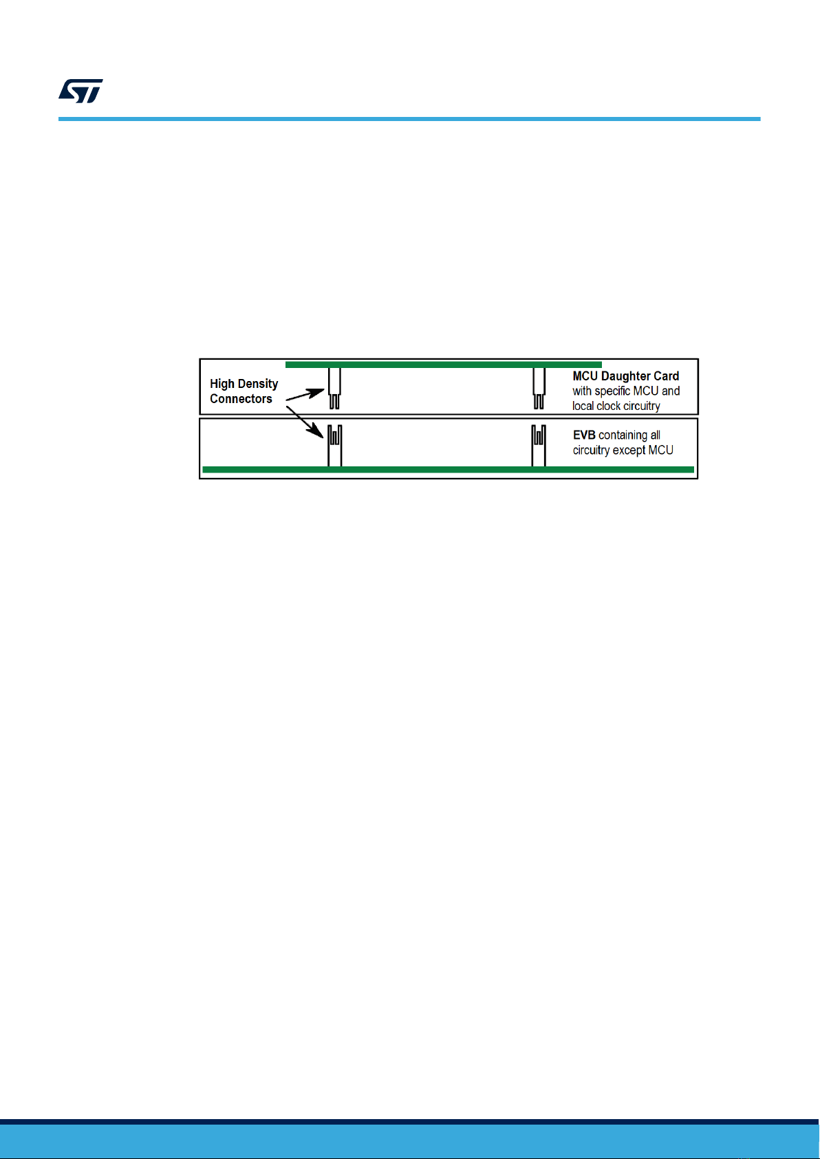
The EVB system consists of a motherboard and a daughter card, both with distinct features.
The mother board provides the following key features:
• Support provided for different SPC58xx MCUs and SPC57xx MCUs by utilizing MCU daughter cards
• Single 12 V external power supply input with four on-board regulators providing all the necessary EVB and
MCU voltages; power supplied to the EVB via a 2.1 mm barrel style power jack or a 2-way level connector
• Master power switch and regulator status LEDs
• Two 240-way high-density daughter card expansion connectors allowing connection of the MCU daughter
card or a custom board for additional application specific circuitry
• All MCU signals readily accessible at a port-ordered group of 0.1” pitch headers
• RS232/SCI physical interface and standard DB9 female connector
• FlexRAY interface
• LINFlexD interface
• CAN FD interfaces (data rates up to 5 Mbit/s), one configurable to be connected to one out of two CAN
modules, and one connected to a dedicated third CAN module
• 10/100 Mbps ethernet interface
• Variable resistor, driving between 5 V and ground
• user switches and 4 user LEDs, freely connectable
• Liberal scattering of GND test points (surface mount loops) placed throughout the EVB
The daughter cards provide the following features:
• MCU (soldered or through a socket)
• Flexible MCU clocking options allow provision of an external clock via SMA connector or 40 MHz EVB
clock oscillator circuit. Jumpers on the daughter card allow selection between these external clocks. SMA
connector on MCU-CLKOUT signal for easy access.
• User reset switch with reset status LEDs
• Standard 14-pin JTAG debug connector and 34-pin Samtec Nexus3+ connector
• 10-pin Serial Interprocessor Interface (SIPI) connector
• Liberal scattering of ground and test points (surface mount loops) placed throughout the EVB
Note: To avoid confusion between jumpers and headers, all EVB jumpers are implemented as 2 mm pitch whereas
headers are 0.1 inch (2.54 mm). This prevents inadvertently fitting a jumper to a header.
4.5 Caution
Before the EVB is used or power is applied, please fully read the following sections on how to correctly configure
the board. Failure to correctly configure the board may cause irreparable component, MCU or EVB damage.
UM2740
EVB features
UM2740 - Rev 1 page 8/45

4.6 Configuration
This section details the configuration of each of the EVB functional blocks.
The EVB has been designed keeping in mind the ease of use, and has been segmented into functional blocks
as shown in the figure below. A detailed silkscreen legend has been used throughout the board to identify all
switches, jumpers and user connectors.
Figure 3. EVB functional blocks
UM2740
Configuration
UM2740 - Rev 1 page 9/45

4.7 Power supply configuration
The EVB requires an external power supply voltage of 12 V DC, minimum 1 A. This allows the EVB to be easily
used in a vehicle if required. The single input voltage is regulated on-board using three switching regulators to
provide the necessary EVB and MCU operating voltages of 5.0 V, 3.3 V and 1.25 V, and one 5 V linear regulator
for the ADC supplies and references.
For flexibility there are two different power supply input connectors on the motherboard as detailed below. There
is also a power supply option on the daughter card to use the daughter card in standalone mode. Please refer to
daughter card documents for details on power input.
4.8 Motherboard power supply connectors
2.1 mm barrel connector – P28:
Figure 4. Power supply barrel connector
2-way lever connector – P32:
Figure 5. 2-lever power connector
This can be used to connect a bare wire lead to the EVB, typically from a laboratory power supply. The
polarization of the connectors is clearly marked on the EVB. A special care must be taken to ensure correct
connection.
UM2740
Power supply configuration
UM2740 - Rev 1 page 10/45

4.9 Regulator power jumpers
There are four power regulator circuits on the SPC58xx motherboard that supply the required voltages to operate
the MCUs:
• 1.25V_SR: 1.25 V switching regulator to supply the core voltage
• 5V_SR: 5 V switching regulator to supply the power management controller, I/O and peripherals
• 3.3V_SR: 3.3 V switching regulator for Ethernet, FlexRAY, debug and I/O
• 5V_LR: 5 V linear regulator for ADC supply and reference
All regulators have the option of being disabled/enabled if they are not required. By default (jumpers are off),
all switching regulators are enabled and the 5 V linear regulator is disabled. The regulators can be enabled
individually by the following jumper settings:
• Connecting J57 enables the 5.0 V linear regulator
• Disconnecting J58 enables the 5.0 V switching regulator
• Disconnecting J59 enables the 3.3 V switching regulator
• Disconnecting J60 enables the 1.25 V switching regulator
The regulators supply power to the daughter cards through the board connector. The individual selection and
configuration of the MCU supplies are done on the daughter cards.
Not all the supported daughter card MCUs require all the supplies to be switched on. Please refer to the individual
daughter card user guide for details.
4.10 Power switch, status LEDs and use
The main power switch (slide switch SW5) can be used to isolate the power supply input from the EVB voltage
regulators if required.
• Moving the slide switch to the right (away from connector P33) will turn the EVB on
• Moving the slide switch to the left (towards connector P33) will turn the EVB off
When power is applied to the EVB, four green power LEDs adjacent to the voltage regulators show the presence
of the supply voltages as follows:
• LED D9 – Indicates that the 5.0 V linear regulator is enabled and working correctly
• LED D11 – Indicates that the 5.0 V switching regulator is enabled and working correctly
• LED D12 – Indicates that the 3.3 V switching regulator is enabled and working correctly
• LED D13 – Indicates that the 1.25 V switching regulator is enabled and working correctly
If no LED is illuminated when power is applied to the EVB and the regulators are correctly enabled using the
appropriate jumpers, it is possible that either power switch SW5 is in the “OFF” position or that the fuse F1 has
blown. The fuse will blow if power is applied to the EVB in reverse-bias, where a protection diode ensures that the
main fuse blows rather than causing damage to the EVB circuitry. If the fuse has blown, check the bias of your
power supply connection then replace fuse F1 with a 20 mm 1.5 A fast blow fuse.
UM2740
Regulator power jumpers
UM2740 - Rev 1 page 11/45

4.11 CAN configuration
The EVB has two high speed CAN FD transceivers and two female standard DB9 connectors to provide physical
CAN FD interfaces for the MCU.
The pinout of the DB9 female connector (J5) is shown in the below figure.
Figure 6. CAN DB9 connector pinout
For flexibility, the CAN FD transceiver I/Os are also connected to two standard 0.1” connectors (P4 and P5) at the
top side of the PCB. The figure below shows the pin-out for these connectors.
Figure 7. CAN 3pin header interface connector
By default, the CAN interfaces are not enabled. To enable the CAN interfaces the jumpers detailed in the table
below need to be placed.
UM2740
CAN configuration
UM2740 - Rev 1 page 12/45

Table 3. CAN control jumpers
Jumper Label Description
J23 CAN2_EN
PHY U2 configuration
1-2: WAKE to GND
3-4: STB to 5 V
5-6: EN to 5 V
J32 CAN2 1-2: PHY TX to MCU
3-4: PHY RX to MCU
J33 CAN-PWR 1-2: 5.0V_SR to PHY U2 VCC
3-4: 12 V to PHY U2 VBAT
J34 INH/ERR
PHY U2 signal out
1: ERR
2: INH
J21 CAN_EN
PHY U1 configuration
1-2: WAKE to GND
3-4: STB to 5 V
5-6: EN to 5 V
J35 CAN-PWR 1-2: 5.0V_SR to PHY U1 VCC
3-4: 12 V to PHY U1 VBAT
J37 TTCAN_TX/MCAN1_TX
PHY U1 TX to MCU
1-2: TTCAN TX
2-3: MCAN1 TX
J38 TTCAN/MCAN1
PHY U1 RX to MCU
1-2: TTCAN RX
2-3: MCAN1 RX
J36 INH/ERR
PHY U1 signal out
1: ERR
2: INH
4.12 RS232 configuration
A female DB9 connector J19 and a RS232 transceiver device provide a physical RS232 interface, allowing a
direct RS232 connection to a PC or terminal.
The figure below shows the pin-out of the RS232 connector. It is to note that the hardware flow control is not
supported on this implementation.
Figure 8. RS232 physical interface connector
UM2740
RS232 configuration
UM2740 - Rev 1 page 13/45

By default the RS232 interface is not enabled. The user needs to place the jumpers detailed in Table 4. RS232
control jumpers to enable the RS232 interface.
Table 4. RS232 control jumpers
Jumper Label Description
J13 SCI TX TX enable
J14 SCI RX RX enable
J25 SCI_PWR Transceiver power on
4.13 LIN configuration
The EVB is fitted with a LIN transceiver (U50) and two different style connectors:
• a standard LIN Molex connector (J14) at the edge of the board
• a standard 0.1" connector (P3).
The figure below shows the pin-out of the Molex connector J4.
Figure 9. LIN molex connector
For flexibility, the LIN transceiver is also connected to a standard 0.1” connector (P3) at the top side of the PCB
as shown in Figure 10. LIN 4pin header interface connector. For ease of use, the 12 V EVB supply is fed to pin1
of P3 and the LIN transceiver power input to pin2. This allows the LIN transceiver to be powered directly from the
EVB supply by simply linking pins 1 and 2 of connector P3 using a 0.1" jumper shunt.
Figure 10. LIN 4pin header interface connector
By default, the LIN interface is not enabled. To enable the LIN interface the jumpers detailed in the table below
need to be placed.
UM2740
LIN configuration
UM2740 - Rev 1 page 14/45

Table 5. LIN control jumpers
Jumper Label Description
J15 LIN_EN LIN PHY (U50) enable
J16 LIN_RX LIN RX enable
J17 LIN_TX LIN TX enable
4.14 FlexRAY configuration
The EVB is fitted with two FlexRAY transceivers, a female DB9 connector (for both transceivers) and two
alternative connectors. Jumpers J27 and J30 are provided to route the respective MCU signals to the physical
interfaces.
The figure below shows the pin-out of the DB9 connector (J2).
Figure 11. FlexRAY DB9 connector pinout
For flexibility, the FlexRAY transceiver is also connected to two FlexRAY connectors (P1 & P2) and two 2pin
Molex connectors (J1 & J3, not populated by default) at the top side of the EVB. the figure below shows the
connections for both types of connectors.
Figure 12. FlexRAY alternative connector pin-outs
By default, the FlexRAY interface is not enabled. To enable the FlexRAY interface the jumpers detailed in the
below table FlexRAY control jumpers need to be placed.
UM2740
FlexRAY configuration
UM2740 - Rev 1 page 15/45

Table 6. FlexRAY control jumpers
Jumper Label Description
J29 FR_PWR
FlexRay transceiver VIO selection
1-2: 12 V to VBAT
3-4: 5V_SR to VCC and VBUF
5-6: 3.3V_SR to VIO
J27 FR_A
1-2: PHY U4 TX to MCU
3-4: PHY U4 TXEN to MCU
5-6: PHY U4 RX to MCU
J28 FR_A
PHY U4 configuration:
1-2: 3.3 V (VIO) to BGE
3-4: 3.3 V (VIO) to EN
5-6: 3.3 V (VIO) to STBY
7-8: GND to WAKE
J30 FR_B
1-2: PHY U5 TX to MCU
3-4: PHY U5 TXEN to MCU
5-6: PHY U5 RX to MCU
J31 FR_B
PHY U5 configuration:
1-2: 3.3 V (VIO) to BGE
3-4: 3.3 V (VIO) to EN
5-6: 3.3 V (VIO) to STBY
7-8: GND to WAKE
UM2740
FlexRAY configuration
UM2740 - Rev 1 page 16/45

4.15 Ethernet configuration
The EVB is fitted with a standard RJ45 Ethernet connector (J7) and an Ethernet transceiver (U6).
By default, the Ethernet interface is not enabled. To enable the Ethernet interface the jumpers detailed in
Table 5. LIN control jumpers need to be placed.
Table 7. Ethernet control jumpers
Jumper Description
J22 PHY power on (jumper placed on default)
J18 RXCLK
J20 CRS_LEDCFG
J24 RXER_MDIXEN
J26 RXDV_MIIMODE
J39 RXD0_PHYAD1
J40 RXD1_PHYAD1
J41 RXD2_PHYAD2
J42 RXD3_PHYAD3
J44 COL_PHYAD0
J45 TXEN
J46 TXCLK
J47 TXD0
J48 TXD1
J49 TXD2
J50 TXD3_SNIMODE
J51 MDC
J52 MDIO
UM2740
Ethernet configuration
UM2740 - Rev 1 page 17/45

4.16 Motherboard test points
Several test points of different shapes and functionalities are scattered around the EVB to allow an easy access
to MCU and reference signals. This chapter summarizes and describes the available test points. Motherboard test
points are listed and detailed in the below table.
Table 8. Test points - motherboard
Signal TP name Shape Description
GND GT1 Hook Ground reference
GND GT2 Hook Ground reference
GND GT3 Hook Ground reference
GND GT4 Hook Ground reference
GND GT5 Hook Ground reference
GND GT6 Hook Ground reference
GND GT7 Hook Ground reference
GND GT8 Hook Ground reference
GND GT9 Hook Ground reference
GND GT10 Hook Ground reference
GND GT11 Hook Ground reference
1.25V_SR JP1 Pin 1.25V_SR reference
1.25V_SR JP2 Pin 1.25V_SR reference
1.25V_SR JP3 Pin 1.25V_SR reference
1.25V_SR JP4 Pin 1.25V_SR reference
3.3V_SR JP5 Pin 3.3V_SR reference
3.3V_SR JP6 Pin 3.3V_SR reference
3.3V_SR JP7 Pin 3.3V_SR reference
3.3V_SR JP8 Pin 3.3V_SR reference
5V_SR JP9 Pin 5V_SR reference
5V_SR JP10 Pin 5V_SR reference
5V_SR JP11 Pin 5V_SR reference
5V_SR JP12 Pin 5V_SR reference
GND JP13 Pin Ground reference
GND JP14 Pin Ground reference
GND JP15 Pin Ground reference
GND JP16 Pin Ground reference
5V_SR TP15 Hook 5V_SR reference
5V_LR TP14 Hook 5V_LR reference
3.3V_SR TP16 Hook 3.3V_SR reference
1.25V_SR TP17 Hook 1.25V_SR reference
FRA-INH2 TP5 Pad FlexRAY
FRA-INH1 TP1 Pad FlexRAY
FRA-ERRN TP2 Pad FlexRAY
FRA-RXEN TP6 Pad FlexRAY
UM2740
Motherboard test points
UM2740 - Rev 1 page 18/45

Signal TP name Shape Description
FRB-INH2 TP7 Pad FlexRAY
FRB-INH1 TP3 Pad FlexRAY
FRB-ERRN TP4 Pad FlexRAY
FRB-RXEN TP8 Pad FlexRAY
FR_DBG0 TP10 Pad FlexRAY debug0
FR_DBG1 TP11 Pad FlexRAY debug1
FR_DBG2 TP12 Pad FlexRAY debug2
FR_DBG3 TP13 Pad FlexRAY debug3
FEC 25MHz TP9 Pad Ethernet clock
UM2740
Motherboard test points
UM2740 - Rev 1 page 19/45

4.17 Board interface connectors
This chapter provides a useful cross reference to see the connection from the motherboard to the board interface
connector, and what MCU pins are connected to the interface connector on the daughter cards.
The Table 7. Ethernet control jumpers lists all the connections to the board interface connector on both
motherboard and daughter cards. The table on the left lists the 240 connections for the first interface connector
(J43), the table on the right lists the 240 connections for the second interface connector (J56): the column
‘Motherboard’ shows the motherboard connections to the interface connectors like power supply connections and
user area port pins.
Ground signals are not listed here. A solid ground connection is achieved through the middle bar of the interface
connector.
Table 9. Board interface connector details
Connector Motherboard Connector Motherboard
A-1 1.25V_SR B-240 1.25V_SR
A-2 1.25V_SR B-239 1.25V_SR
A-3 1.25V_SR B-238 1.25V_SR
A-4 1.25V_SR B-237 1.25V_SR
A-5 PA0 B-236 PB0
A-6 PA1 B-235 PB1
A-7 PA2 B-234 PB2
A-8 PA3 B-233 PB3
A-9 PA4 B-232 PB4
A-10 PA5 B-231 PB5
A-11 PA6 B-230 PB6
A-12 PA7 B-229 PB7
A-13 PA8 B-228 PB8
A-14 PA9 B-227 PB9
A-15 PA10 B-226 PB10
A-16 PA11 B-225 PB11
A-17 PA12 B-224 PB12
A-18 PA13 B-223 PB13
A-19 PA14 B-222 PB14
A-20 PA15 B-221 PB15
A-21 5.0V_SR B-220 5.0V_SR
A-22 5.0V_SR B-219 5.0V_SR
A-23 5.0V_SR B-218 5.0V_SR
A-24 5.0V_SR B-217 5.0V_SR
A-25 PC0 B-216 PD0
A-26 PC1 B-215 PD1
A-27 PC2 B-214 PD2
A-28 PC3 B-213 PD3
A-29 PC4 B-212 PD4
A-30 PC5 B-211 PD5
A-31 PC6 B-210 PD6
UM2740
Board interface connectors
UM2740 - Rev 1 page 20/45
Table of contents
Other ST Motherboard manuals

ST
ST STEVAL-TSP009V2 Administrator Guide

ST
ST STM32F779I-EVAL User manual

ST
ST M24LR64-R User manual

ST
ST STEVAL-OET001V1 User manual

ST
ST EVAL-L9963E-MCU User manual

ST
ST STM3241G-EVAL User manual

ST
ST STM32L476G-EVAL User manual

ST
ST STM32303E-EVAL User manual

ST
ST STEVAL-IPC002V1 User manual

ST
ST M24LR-DISCOVERY User manual