ST STM32L4P5G-DK User manual

Introduction
The STM32L4P5G-DK Discovery kit is a complete demonstration and development platform for the STMicroelectronics Arm®
Cortex®-M4 core-based STM32L4P5AGI6P microcontroller with four I2C buses, three SPI and six USART ports, CAN port, two
SAI ports, 12-bit ADC, 12-bit DAC, internal 320-Kbyte SRAM and 1-Mbyte flash memory, two Octo‑SPI memory interfaces,
touch-sensing capability, USB OTG FS port, TFT LCD controller, flexible memory controller (FMC), 8- to 14-bit DCMI interface,
and JTAG debugging support.
The STM32L4P5G-DK Discovery kit is used as a reference design for user application development before porting to the final
product.
The full range of hardware features on the board helps the user evaluate all the peripherals (USB OTG FS, Octo‑SPI flash
memory and PSRAM memory device, eMMC, and others) and develop applications. The ARDUINO® Uno V3 and STMod+
connectors provide easy connection to extension shields or daughterboards for specific applications.
STLINK-V3E is integrated into the board, as an embedded in-circuit debugger and programmer for the STM32 MCU and the
USB Virtual COM port bridge.
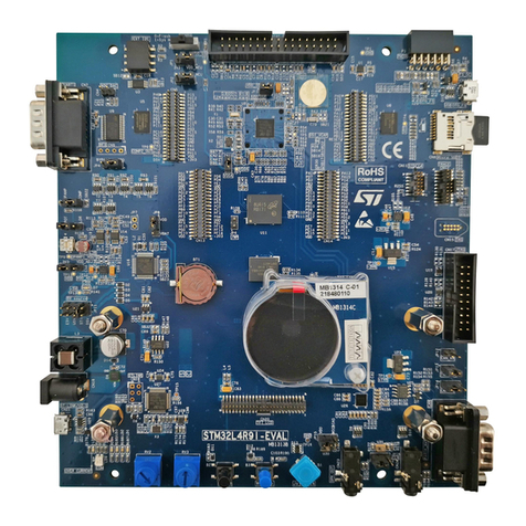
Figure 1. STM32L4P5G-DK top view Figure 2. STM32L4P5G-DK bottom view
Pictures are not contractual.
Discovery kit with STM32L4P5AG MCU
UM2651
User manual
UM2651 - Rev 3 - October 2023
For further information contact your local STMicroelectronics sales office. www.st.com

1 Features
• STM32L4P5AGI6P Arm® Cortex® core-based microcontroller featuring 1 Mbyte of flash memory and 320
Kbytes of RAM in a UFBGA169 package
• 240x240 64‑bit color LCD with RGB interface (connector only)
• 4-Gbyte onboard eMMC
• On-board current measurement
• SAI audio codec (footprint only)
• MEMS digital microphone (footprint only)
• 512-Mbit Octo‑SPI NOR flash memory with DDR mode
• 64-Mbit Octo‑SPI PSRAM memory with DDR mode
• 2 user LEDs
• Reset buttons
• 4-direction joystick with a selection button
• Board connectors:
– 8-bit camera (footprint only)
– Stereo headset jack (footprint only)
– USB with Micro-AB
– User interface through USB Virtual COM port
– Arm® Cortex® 10-pin 1.27 mm-pitch debug connector over STDC14 footprint
– ARDUINO® Uno V3 expansion connector
– STMod+ expansion connector
• Flexible power‑supply options:
– ST-LINK USB VBUS, USB OTG connector, or external sources
• On-board STLINK-V3E debugger/programmer with USB re-enumeration capability: mass storage, Virtual
COM port, and debug port
• Microcontroller supply voltage: fixed 3.3 V and extern SMPS to generate Vcore logic supply
• Comprehensive free software libraries and examples available with the STM32CubeL4 MCU Package
• Support of a wide choice of Integrated Development Environments (IDEs) including IAR Embedded
Workbench®, MDK-ARM, and STM32CubeIDE
Note: Arm is a registered trademark of Arm Limited (or its subsidiaries) in the US and/or elsewhere.
UM2651
Features
UM2651 - Rev 3 page 2/37

2 Ordering information
To order the STM32L4P5G-DK Discovery kit, refer to Table 1. Additional information is available from the
datasheet and reference manual of the target STM32.
Table 1. Ordering information
Order code Board references Target STM32
STM32L4P5G-DK • MB1535(1)
• MB1280(2) STM32L4P5AGI6P
1. Main board.
2. Fanout board.
2.1 Codification
The meaning of the codification is explained in Table 2.
Table 2. Codification explanation
STM32XXYYZ-DK Description Example: STM32L4P5G-DK
XX MCU series in STM32 32-bit Arm Cortex MCUs STM32L4+ series
YY MCU product line in the series STM32L4P5
ZSTM32 flash memory size:
• G for 1 Mbyte 1 Mbyte
DK Discovery kit Discovery kit
UM2651
Ordering information
UM2651 - Rev 3 page 3/37

3 Development environment
3.1 System requirements
•Multi‑OS support: Windows® 10, Linux® 64-bit, or macOS®
• USB Type-A or USB Type-C® to Micro-B cable
Note: macOS® is a trademark of Apple Inc., registered in the U.S. and other countries and regions.
Linux® is a registered trademark of Linus Torvalds.
Windows is a trademark of the Microsoft group of companies.
3.2 Development toolchains
•IAR Systems® - IAR Embedded Workbench®(1)
•Keil® - MDK-ARM(1)
• STMicroelectronics - STM32CubeIDE
1. On Windows® only.
3.3 Demonstration software
The demonstration software, included in the STM32Cube MCU Package corresponding to the on-board
microcontroller, is preloaded in the STM32 flash memory for easy demonstration of the device peripherals in
standalone mode. The latest versions of the demonstration source code and associated documentation can be
downloaded from www.st.com.
UM2651
Development environment
UM2651 - Rev 3 page 4/37

4 Conventions
Table 3 provides the conventions used for the ON and OFF settings in the present document.
Table 3. ON/OFF convention
Convention Definition
Jumper JPx ON Jumper fitted
Jumper JPx OFF Jumper not fitted
Jumper JPx [1-2] Jumper fitted between Pin 1 and Pin 2
Solder bridge SBx ON SBx connections closed by 0 Ω resistor
Solder bridge SBx OFF SBx connections left open
Resistor Rx ON Resistor soldered
Resistor Rx OFF Resistor not soldered
Capacitor Cx ON Capacitor soldered
Capacitor Cx OFF Capacitor not soldered
UM2651
Conventions
UM2651 - Rev 3 page 5/37

5 Delivery recommendations
Before the first use, check the board for any damage that might have occurred during shipment, and check that all
socketed components are firmly fixed in their sockets and that none is loose in the plastic bag.
UM2651
Delivery recommendations
UM2651 - Rev 3 page 6/37

6 Hardware layout and configuration
The STM32L4P5G-DK Discovery kit is designed around the STM32L4P5AGI6P target microcontroller. Figure 3
illustrates STM32L4P5AGI6P connections with peripheral components. Figure 4 shows the location of the main
components on the top side of the Discovery board and Figure 5 shows the location of the main components on
the bottom side of the Discovery board.
Figure 3. STM32L4P5G-DK hardware block diagram
DT53251V1
STM32L4P5AGI6P
3.3 V
Audio codex
RTC
DAP
32 KHz crystal
VBAT
STLINK-V3E
I2C1
SAI1
LEDs
eMMC
Joystick,
buttons
GPIO
SDMMC1
USB connector OTG FS
OctoSPI2
Octo-SPI
flash memory
USART1
DFSDM
3.3 V power
supply
1.8 V power
supply
RGB TFT LCD
STMod+
connector
OctoSPI1
Octo-SPI
PSRAM
MEMs
DCMI
Camera
connector
PIR
ARDUINO®
connector
Touch panel
MFX
SMPS power
supply
Note: The gray features are not soldered. Only footprints are present on the board.
UM2651
Hardware layout and configuration
UM2651 - Rev 3 page 7/37

Figure 4. STM32L4P5G-DK PCB layout (top view)
DT53252V1
SWCLK and SWDIO
(CN2)
STMod+ connector
(CN1)
STLINK-V3E
overcurrent alarm
(LD3)
Camera connector
(CN5)
STM32L4P5AGI6P
(U8)
User LEDs
(LD1 and LD2)
ST-LINK SWD
(CN4)
STLINK-V3E COM
(LD4)
5V PWR
(LD5)
STDC14 connector
(CN6)
USB-OTG overcurrent
(LD6)
USB-OTG
(LD7)
USB-OTG connector
(CN7)
5V source selection
(JP4)
LCD connector
(CN9)
External SMPS selection
(CN8)
UM2651
Hardware layout and configuration
UM2651 - Rev 3 page 8/37

Figure 5. STM32L4P5G-DK PCB layout (bottom view)
DT53253V1
STLINK-V3E switcher
(SW1)
ARDUINO® connector
(CN13 and CN15)
MFX SWD
(CN17)
STLINK-V3E USB
(CN11)
ARDUINO® LED
(LD8)
Audio OUT
(CN16)
ARDUINO® connector
(CN12 and CN14)
UM2651
Hardware layout and configuration
UM2651 - Rev 3 page 9/37

6.1 Embedded STLINK-V3E
6.1.1 Description
The STLINK-V3E facility for debugging and programming the STM32L4P5AGI6P is integrated into the
STM32L4P5G-DK board. It supports the following features:
• Self-powered through a USB connector (Micro-B)
• USB 2.0 high-speed compatible interface
• Direct firmware update support (DFU)
• SWD and serial wire viewer (SWV) communication support
• Drag-and-drop flash memory programming
• Two colored LEDs: communication and power
The USB connector (CN11) can be used to power the STM32L4P5G-DK regardless of the STLINK-V3E facility
used for debugging or programming STM32L4P5AGI6P. This holds also when the STLINK-V3E standalone tool is
connected to CN6 and used for debugging or programming STM32L4P5AGI6P. Section 6.2 Power supply
provides more detail about powering STM32L4P5G-DK. Refer to www.st.com for details about STLINK-V3E.
6.1.2 Drivers and firmware upgrade
The STLINK-V3E requires drivers to be installed on Windows®. It embeds firmware that needs to be updated to
benefit from new functionalities or corrections. Refer for details to the technical note Overview of ST-LINK
derivatives TN1235.
6.1.3 Virtual COM port
The serial interface USART2 (PA2 and PA3 ports) is directly available as a Virtual COM port of the PC, connected
to the STLINK-V3E USB connector (CN11). The Virtual COM port settings are 115200 bps, 8-bit data, no parity,
one stop bit, and no flow control.
6.2 Power supply
The STM32L4P5G-DK Discovery kit is designed to be powered from a 5 V DC power source. One of the following
four 5 V DC power inputs can be used, upon appropriate board configuration:
• Micro-B USB receptacle (CN11) of STLINK-V3E with enumeration. Up to 500 mA can be supplied to the
board (JP4 jumper setting on STLK on the silkscreen). This offers the enumeration feature described in
Section 6.2.1.
• Micro-B USB receptacle (CN11) of STLINK-V3E without enumeration. Up to 1000 mA can be supplied to
the board directly without enumeration (JP4 jumper setting on CHGR on the silkscreen).
• Micro-AB USB receptacle (CN7) of the USB OTG FS interface. Marked USB_OTG on the board (JP4
jumper setting on U5V on the silkscreen). Up to 500 mA can be supplied to the board in this way.
• 7 to 12 V DC power from CN13 pin8: Named VIN on silkscreen, the extension connectors for ARDUINO®
Uno shields (JP4 setting on external power source on silkscreen (E5V)).
The LD5 green LED turns on when the voltage on the power line marked as 5 V is present. All supply lines
required for the operation of the components on the STM32L4P5G-DK are derived from that 5 V line.
Table 4 describes the settings of all jumpers related to powering the STM32L4P5G-DK and extension board.
VDD_MCU is a STM32L4P5AGI6P digital supply voltage line. It can be connected to a fixed 3.3 V voltage supply.
6.2.1 Supplying the board through the STLINK-V3E USB port
To power the STM32L4P5G-DK this way, the PC USB Host gets connected to the Micro-B USB receptacle of the
STM32L4P5G-DK board via a USB cable. The connection event starts with the USB enumeration procedure. In
its initial phase, the current supply capability of the USB Host port is limited to 100 mA. It is enough because only
the STLINK-V3E part of the STM32L4P5G-DK draws power at that time: The U2 power switch is set to the OFF
position, which isolates the rest of the STM32L4P5G-DK from the power source. In the next phase of the
enumeration procedure, the host PC informs the STLINK-V3E facility of its capability to supply current up to
300 mA. If the answer is positive, the STLINK-V3E sets the U2 power switch to the ON position to supply power
to the rest of the STM32L4P5G-DK board. If the PC USB port is not capable of supplying current up to 300 mA,
the CN13 pin8 (VIN) can be used to supply the board instead.
UM2651
Embedded STLINK-V3E
UM2651 - Rev 3 page 11/37

If a short circuit occurs on the board, the power switch protects the USB port of the host PC against a current
demand exceeding 500 mA. In such an event, the LD3 LED lights up.
The STM32L4P5G-DK board can also be supplied from a USB power source not supporting enumeration, such
as a USB charger. In this particular case, the JP4 jumper must be ON as shown in Table 4. Power‑supply‑related
jumper and solder bridge settings. STLINK-V3E bypasses power, regardless of enumeration procedure results,
and passes the power unconditionally to the board.
The LD5 green LED turns on whenever the whole board is powered.
6.2.2 Using STLINK-V3E along with powering through external power
The board might require more than 300 mA of supply current. It cannot be supplied by a host PC connected to the
STLINK-V3E USB port for debugging or programming the STM32L4P5AGI6P. In such a case, the board can be
supplied through CN13 pin8 (marked VIN on the board).
To do this, it is important to power the board before connecting it with the host PC, which requires the following
sequence to be respected:
1. Set the JP4 jumper in the E5V position,
2. Connect the external power source to CN13 pin8,
3. Check that the LD5 green LED is turned on,
4. Connect the host PC to the USB connector (CN11).
Caution: In case the board demands more than 300 mA and the host PC is connected via USB before the board is
powered from CN13 pin8, there is a risk that the following events to occur (listed in reverse severity order):
1. The host PC can supply 300 mA (the enumeration succeeds) but it features no overcurrent protection on
its USB port. It is damaged due to an overcurrent.
2. The host PC can supply 300 mA (the enumeration succeeds) and it has built-in overcurrent protection on
its USB port, limiting or shutting down the power out of its USB port when the excessive current demand
from the USB port is detected. This causes an operating failure of the STM32L4P5G-DK.
3. The host PC cannot supply 300 mA (the enumeration fails). The STLINK-V3E does not supply the rest of
the necessary current from its USB port VBUS line.
Table 4 details the jumper and solder bridge settings used for the power supply configuration of the
STM32L4P5G-DK.
Table 4. Power‑supply‑related jumper and solder bridge settings
Jumper/solder
bridge Setting Configuration(1)
JP4 5 V source
selector
STLK U5V E5V D5V CHGR
Default setting.
STM32L4P5G-DK is supplied through the Micro-B USB
receptacle (CN11). It depends on the host PC USB port’s
powering capability declared in the enumeration.
STLK U5V E5V D5V CHGR
STM32L4P5G-DK is supplied through the Micro-AB USB
receptacle (CN7).
STLK U5V E5V D5V CHGR
STM32L4P5G-DK is supplied through CN13 pin 8.
STLK U5V E5V D5V CHGR
STM32L4P5G-DK is supplied through CN13 pin 5.
STLK U5V E5V D5V CHGR
STM32L4P5G-DK is supplied through the Micro-B USB
receptacle (CN11).
This setting is applied to power the board through CN11 using
a USB charger.
UM2651
Power supply
UM2651 - Rev 3 page 12/37

Jumper/solder
bridge Setting Configuration(1)
R46 VBAT
connection
R46 ON Default setting.
VBAT is connected to VDD_MCU.
R46 OFF VBAT is not connected to VDD_MCU.
JP2 VDDA /
VDDUSB
connection
13
2Default setting.
VDDA and VDDUSB terminal of STM32L4P5AGI6P are
connected to VDD_MCU.
13
2VDDA and VDDUSB terminals of STM32L4P5AGI6P are
connected to 3V3.
JP6 3V3
12Default setting.
The board is connected to a fixed 3V3.
12
The device is connected to measure current consumption.
1. On all STLINK-V3E boards, the target application is now able to run even if the STLINK-V3E is either not connected to a
USB Host, or is powered through a USB charger or a nonenumerating USB Host.
6.2.3 SMPS power supply
VDD12 is the external power supply bypassing the internal regulator when connected to an external SMPS. The
board is populated with a DC-DC regulator mounted on the U22 footprint, which allows to supply dynamically the
VDD12 pins in Run, Sleep, and Stop 0 modes at a voltage range from 1.0 to 1.35 V by configured
STM32L4P5AGI6P GPIOs (PH2, PH4, and PH13).
6.3 Clock references
Two clock references are available on the STM32L4P5G-DK for the STM32L4P5AGI6P target microcontroller.
• 32.768 kHz crystal X2, for embedded RTC
• 24 MHz crystal X3, for main clock generator (footprint only)
The main clock generation is possible via an internal RC oscillator (default) or from STLK_MCO, disconnected by
removing resistors R49, R51, and R52 when the internal RC clock is used.
6.4 Reset source
The general reset of the STM32L4P5G-DK Discovery kit is active LOW. Sources of reset are:
• B2 RESET button
• STDC14 connector (CN6), reset from debug tools
• ARDUINO® Uno shield board through CN13
• Embedded STLINK-V3E
6.5 Boot option
After reset, the STM32L4P5AGI6P MCU can boot from the following embedded memory locations:
• Main (user, nonprotected) flash memory
• System (protected) flash memory
• RAM, for debugging
The boot option is configured by setting PH3 (BOOT0) and the boot base address programmed in the nBOOT1,
nBOOT0, and nSWBOOT0 of FLASH_OPTR option bytes.
Table 5 describes the hardware configuration for the Boot mode.
UM2651
Clock references
UM2651 - Rev 3 page 13/37

Table 5. Boot selection switch
Resistor Setting(1) Description
R37 and R38
R37 OFF
R38 ON
The BOOT0 line is tied LOW. STM32L4P5AGI6P boots from the main
flash memory.
R37 ON
R38 OFF
The BOOT0 line is tied HIGH. STM32L4P5AGI6P boots from system flash
memory (nBOOT1 bit of FLASH_OPTR register is set HIGH) or from RAM
(nBOOT1 is set to LOW).
1. The default configuration is shown in bold.
6.6 Audio (footprint only)
An audio codec, connected to the SAI interface of STM32L4P5AGI6P, offers the possibility to connect a stereo
headphone or headset with a mono analog microphone. The codec communicates with STM32L4P5AGI6P via
the I2C1 bus, which is shared with MFX and JDI LCD.
The I2C-bus addresses of the codec are 0x95 and 0x94.
6.7 Digital microphones (footprint only)
Two MEMS digital microphones, U17 and U23, are available on STM32L4P5G-DK. The two microphones are
located at a distance of 21 mm from each other. They are connected to the STM32 DFSDM by the PE9 port,
generating the clock, and by the PD3 port, collecting the PDM interleaved data.
6.8 USB FS port
The STM32L4P5G-DK Discovery kit supports USB OTG FS, full-speed communication, via the USB Micro-AB
receptacle (CN7) and the USB power switch (U7) connected to VBUS.
An LD7 green LED lights up in one of the following cases:
• The power switch (U7) is ON and STM32L4P5G-DK works as a USB Host.
• VBUS is powered by another USB Host when STM32L4P5G-DK works as a USB Device.
The LD6 red LED is lit in case of overcurrent.
6.9 User LEDs
Two general-purpose color LEDs, LD1 and LD2, are available as light indicators. Each LED is in the light-emitting
state with a low level of the corresponding ports of the STM32L4P5AGI6P MCU.
6.10 Physical input devices
The STM32L4P5G-DK board provides several input devices for physical human control.
• A four-way joystick controller with a select key (B1)
• A reset button (B2)
6.11 Octo‑SPI device
U12, a 512-Mbit Octo‑SPI user flash memory, is connected to the OCTOSPIM_P2 interface of
STM32L4P5AGI6P.
U11, a 64-Mbit Octo‑SPI PSRAM memory, is connected to the OCTOSPIM_P1 interface of STM32L4P5AGI6P.
By default, U14 is the footprint of a Quad-SPI interface for the SO‑8 package. Note that U11 and U14 share the
same GPIO port for Octo‑SPI and Quad-SPI interface usage.
6.12 eMMC
The STM32L4P5G-DK Discovery kit embeds a 4-Gbyte eMMC chip. It is connected to the STM32L4P5AGI6P
SDMMC1 port.
UM2651
Audio (footprint only)
UM2651 - Rev 3 page 14/37

6.13 MFX MCU
The MFX MCU is used as an MFX multifunction expander and an IDD measurement calculator.
6.13.1 MFX
The MFX circuit on the STM32L4P5G-DK Discovery kit acts as an I/O expander. The communication interface
between MFX and STM32L4P5AGI6P is the I2C1 bus. The signals connected to MFX are listed in Table 6.
Table 6. MFX signals
MFX pin
number
MFX pin
name MFX function STM32L4P5G-DK function MFX direction Terminal device
15 PA5 MFX_GPIO5 Camera_Flash Output Camera
16 PA6 MFX_GPIO6 Camera_STANDBY Output Camera
17 PA7 MFX_GPIO7 Camera_PLUG Input Camera
18 PB0 MFX_GPIO0 USB_PSON Output USB OTG FS
19 PB1 MFX_GPIO1 USB_OVRCR Input USB OTG FS
20 PB2 MFX_GPIO2 Audio_RST Input Audio
26 PB13 MFX_GPIO13 - - -
27 PB14 MFX_GPIO14 - - -
28 PB15 MFX_GPIO15 - - -
29 PA8 MFX_GPIO8 - - -
30 PA9 MFX_GPIO9 - - -
31 PA10 MFX_GPIO10 - - -
32 PA11 MFX_GPIO11 - - -
33 PA12 MFX_GPIO12 - - -
39 PB3 MFX_GPIO3 Camera_RST Output Camera
40 PB4 MFX_GPIO4 Camera_Shutter Output Camera
6.13.2 IDD measurement
STM32L4P5AGI6P has a built-in circuit to measure its current consumption (IDD) in Run and Low‑power modes,
except Shutdown mode. It is strongly recommended that the MCU supply voltage (VDD_MCU line) does not
exceed 3.3 V because there are components on the STM32L4P5G-DK supplied from 3.3 V that communicate
with the MCU through I/O ports. Voltage exceeding 3.3 V on the MCU output port may inject current into 3.3 V
supplied peripheral I/Os and distort the MCU current-consumption measurement.
Table 7 shows the setting of the jumper associated with the IDD measurement on the board.
Table 7. IDD measurement‑related jumper setting
Jumper Setting(1) Configuration
JP5
JP5 [1-2] STM32L4P5AGI6P has a built-in circuit to measure its current
consumption.
JP5 [2-3] IDD measurement is not available, bypass mode only for STM32L4P5AGI6P
VDD_MCU power supply.
1. The default configuration is shown in bold.
6.14 LCD interface (connector only)
STM32L4P5G-DK supports a 6‑bit RGB interface and a touch-panel interface. The users may develop their
daughterboard, plugged into CN9, for application.
UM2651
MFX MCU
UM2651 - Rev 3 page 15/37

6.15 Camera connector (CN5) (footprint only)
A connector for 8- to 12-bit DCMI signals on the STM32L4P5G-DK Discovery kit supports a camera module
daughterboard MB1183 or MB1379. The camera shares the I2C4 bus with the STMod+ and ARDUINO®
connectors.
UM2651
Camera connector (CN5) (footprint only)
UM2651 - Rev 3 page 16/37

7 Connectors
7.1 STMod+ connector (CN1)
The standard 20-pin STMod+ connector is available on the STM32L4P5G-DK Discovery kit to increase
compatibility with external boards and modules from the ecosystem of microcontrollers. By default, it is designed
to support an ST-dedicated fanout board to connect different modules or board extensions from different
manufacturers. The fanout board also embeds a 3.3 V regulator and I2C level shifter (footprint only). Schematics
of the fanout board are available at the www.st.com website.
For details about the STMod+ interface, refer to the technical note STMod+ interface specification TN1238.
Figure 7. STMod+ connector (CN1) front view
Table 8. STMod+ connector (CN1) pinout
Pin number Description Pin number Description
1 SPI1_NSS/USART3_CTS (PG5/PD11) 11 INT (PD10)
2 SPI1_MOSI/ USART3_TX (PG4/PD8) 12 RESET (PF11)
3 SPI1_MISO/ USART3_RX (PG3/PD9) 13 ADC (PA5)
4 SPI1_SCK/ USART3_RTS (PG2/PD12) 14 PWM (PG11)
5 GND 15 5 V
6 5 V 16 GND
7 I2C4_SCL (PF14) 17 DFSDM1-CKOUT (PF10)
8 SPI1_MOSIs (PE15) 18 DFSDM1- DATIN1 (PB12)
9 SPI1_MISOs (PE14) 19 GPIO3 (PD0)
10 I2C4_SDA (PF15) 20 GPIO4 (PD1)
7.2 STLINK-V3E programming connector (CN4)
This connector is only used for embedded STLINK-V3E programming during board manufacturing. It is not
populated by default and not for the end-user.
UM2651
Connectors
UM2651 - Rev 3 page 17/37

7.3 Camera module connector (footprint only) (CN5)
Figure 8. Camera module connector (CN5) top view
Table 9. Camera module connector (CN5) pinout
Pin number Description Pin number Description
1 1V8 2 1V8
3 GND 4 GND
5 DCMI_D10 (PI3) 6 DCMI_D11 (PH15)
7 GND 8 GND
9 DCMI_D8 (PH6) 10 DCMI_D9 (PH7)
11 GND 12 GND
13 I2C4_SCL (PF14) 14 I2C4_SDA (PF15)
15 Camera_PLUG (MFX GPIO7) 16 GND
17 Camera_RST (MFX GPIO3) 18 -
19 Camera_STANDBY (MFX GPIO6) 20 Camera_CLK
21 GND 22 GND
23 DCMI_D0 (PH9) 24 DCMI_D1 (PH10)
25 DCMI_D2 (PE0) 26 DCMI_D3 (PH12)
27 DCMI_D4(PH14) 28 DCMI_D5 (PI4)
29 DCMI_D6 (PI6) 30 DCMI_D7 (PI7)
31 DCMI_HSYNC (PH8) 32 DCMI_VSYNC (PI5)
33 DCMI_PIXCLK (PH5) 34 -
35 Camera_Shutter (MFX GPIO4) 36 Camera_Flash (MFX GPIO5)
37 GND 38 GND
39 2V8 40 2V8
UM2651
Camera module connector (footprint only) (CN5)
UM2651 - Rev 3 page 18/37

7.4 STDC14 connector (CN6)
Figure 9. STDC14 debugging connector (CN6) top view
Table 10. STDC14 debugging connector (CN6) pinout
Terminal Function/MCU port Terminal Function/MCU port
1 - 2 -
3 VDD 4 SWDIO/TMS (PA13)
5 GND 6 SWDCLK/TCK (PA14)
7 GND 8 SWO/TDO (PB3)
9 - 10 -
11 GND 12 RESET#
13 VCP_RX_STDC (PA3) 14 VCP_TX_STDC (PA2)
7.5 USB OTG FS Micro-AB connector (CN7)
A USB OTG full‑speed communication link is available at the USB Micro-AB receptacle connector (CN7). The
Micro-AB receptacle enables USB Host and Device features.
Figure 10. USB OTG FS Micro-AB connector (CN7) front view
Table 11. USB OTG FS Micro-AB connector (CN7) pinout
Pin number Description Pin number Description
1 VBUS 4 ID
2 DM 5 GND
3 DP - -
UM2651
STDC14 connector (CN6)
UM2651 - Rev 3 page 19/37

7.6 STLINK-V3E USB Micro-B connector (CN11)
The USB connector (CN11) is used to connect the onboard STLINK-V3E facility to the PC for flashing and
debugging software.
Figure 11. Micro-B connector (CN11) top view
Table 12. USB Micro-B connector (CN11) pinout
Terminal Description Terminal Description
1 VBUS (power) 4 ID
2 DM 5 GND
3 DP 6 - 11 Shield
UM2651
STLINK-V3E USB Micro-B connector (CN11)
UM2651 - Rev 3 page 20/37
Table of contents
Other ST Motherboard manuals

ST
ST Nucleo STM32F302R8 User manual

ST
ST TN100 RF User manual

ST
ST AEKD-USBTYPEC1 User manual

ST
ST STEVAL-WBC86TX User manual

ST
ST STM32F407 Series User manual

ST
ST STM320518-EVAL User manual

ST
ST UM2335 User manual

ST
ST STM32CubeH7 User manual

ST
ST STM32L073Z-EVAL User manual

ST
ST NUCLEO-WL55JC STM32WL User manual

ST
ST STM3210E-EVAL User manual

ST
ST STEVAL-IHM022V1 User manual

ST
ST M24LR64-R User manual

ST
ST STEVAL-ILL059V1 User manual

ST
ST UM2414 User manual

ST
ST STM3210B-EVAL User manual
ST
ST eMotion STEVAL-MKI109V1 User manual

ST
ST ST72F651 User manual

ST
ST STEVAL-IHM011V1 User manual

ST
ST STM32 Nucleo Installation and operating instructions