Section
2~85/R485
Service
OPERATING
INFORMATION
PRELIMINARY
INFORMATION
The
485
is
cooled by air entering through the air filter
on the rear panel and exiting through the holes on the sides.
Adequate clearance must be provided at these locations.
Allow at least one inch clearance behind the air filter and at
least one inch on the sides.
Athermal
cutoot
in
this instrument provides thermal
protection and disconnects the power
to
the instrument
if
the internal temperature exceeds asafe operating level.
Power
is
automatically restored
.......
en the temperature
returns to asafe level.
Oean
the air filter periodically: a
dirtY filter prevents adequate air flow into
the
instrument.
Operating Temperature
The
485
can be operated where the ambient air
temperature
is
between
-ls'"C
and +5s'"C (+5°F
and
+131°F). This instrument can
be
stored in ambient
temperatures between
-5s'"C
and +75°C
(-67°F
and
+167"F). After storage at temperatures beyond the opera·
ting limits, allow the chassis temperature
to
come within
the operating limits before power
is
applied.
WARNING
I
This instrument
is
designed
for
operation from a
power source with irs nautra'
at
or
near earth
(ground) potential
with
aseparate safety-earth
conductor.
It
is
not
intended
for
operarion from two
phases
of
amulti-phase sysrem,
or
across the
legs
of
a
single-phase, three-wire system.
Operating Voltage
-----,
The
485
can be operated from either a115 Vor 230 V
nominal line voltage source,
or
a220 Vellternal battery
pack. The Line Voltage Selector switch on the rear panel
converts this instrument from one operating voltage
to
the
other.
General
To effectively use the 485, the operation and capabilities
of the instrument
must
be known. This section describes
the operation of the controls and connections and gives
first-time and general operating information.
CONTROLS ANO CONNECTORS
Power Cord Conductor Identification General
Conductor Color Alternate Color
Ungrounded (Line) Brown Black
Grounded (Neutral) Blue
lftfhite
Grounding (Earthlngl Green·Yellow Green·Yellow
~
This instrument
may
be
damaged
if
operated
with
the
Line Vo/rage $elector switch
set
to
incorrect posi-
tions
for
the line volrage applied.
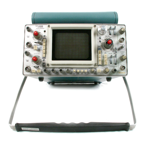
The major controls and connectors for operation of lhe
485
are located on the front panel of the instrument. Some
aU;l{iliary
functions are provided on the side, top,
bonom
and rear panel. To make
full
use of the capabilities of this
instrument,
the
operator should be familiar with the
function and use of each of these controls and connectors.
Abrief description of each control and connector
is
given
here.
Front Panel
POWER
Pushbutton Turns instrument on or off.
115 V
230
V9(J.136 V
180-272 V
CAL 5 V Connector
BNC
connector for square·wave
voltage calibrator
output
signal.
The
485
is
designed to
be
used with athree-wire
AC
power system.
If
the three
to
two·wire adapter
is
used
to
connect this instrument to atwo-wire
AC
power system, be
sure
to
connect the groond lead of the adapter
to
earth
(ground). Failure
to
complete the groond
sV1tem
may allow
;he chassis of this instrument
to
be elevated above ground
potential and pose ashock hazard.
FREO Pushbutton
INTENSITY Control
BINTENSITY
Control
Selects one of
two
frequencies
11
kHz or 1
MHz)
for the last-fise
calibrator signal.
Controls intensitY of writing beam.
Provides additional intensitY coo-
trol for the BSWEEP.
AEV.C,MAA.1977
2·'
