manuals.online logo
Brands
  1. Home
  2. •
  3. Brands
  4. •
  5. Texas Instruments
  6. •
  7. Control Unit
  8. •
  9. Texas Instruments DRV2605LEVM-MD User manual

Texas Instruments DRV2605LEVM-MD User manual

TI Confidential – NDA Restrictions
User's Guide
SLOU400–September 2014
DRV2605L Multi-Driver ERM, LRA Haptic Driver Evaluation
Kit User’s Guide
1 Introduction
The DRV2605L device is a haptic driver designed for linear resonant actuators (LRA) and eccentric
rotating mass (ERM) motors. The device has many features that help eliminate the design complexities of
haptic motor control including:
• Reduced solution size
• High-efficiency output drive
• Closed-loop motor control
• Quick device startup
• Embedded waveform library
• Auto-resonance frequency tracking
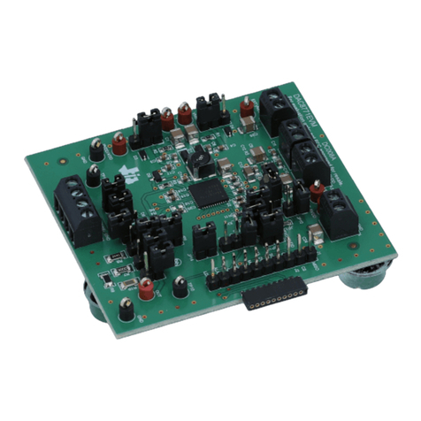
The DRV2605LEVM-MD evaluation module (EVM) is an evaluation platform for the DRV2605LDGS. The
kit includes an MSP430F5510 microcontroller (MCU), terminal output support for up tight LRAs or ERMs,
sample waveforms provided by Immersion, and capacitive touch buttons which demonstrate the
capabilities of the DRV2605L.
This user’s guide contains instructions for setting up and operating the DRV2605LEVM-MD.
Figure 1. DRV2605LEVM
Code Composer Studio is a trademark of Texas Instruments.
All other trademarks are the property of their respective owners.
1
SLOU400–September 2014 DRV2605L Multi-Driver ERM, LRA Haptic Driver Evaluation Kit User’s Guide
Submit Documentation Feedback Copyright © 2014, Texas Instruments Incorporated
TI Confidential – NDA Restrictions
USB VBAT
SBW
MSP430
OUT8 OUT7 OUT6 OUT5
OUT4OUT3OUT2
OUT1
DRV2605L
DRV2605L DRV2605L DRV2605L DRV2605L
DRV2605L DRV2605L DRV2605L
BSL RESET
USER SW
TCA9548A
TCA9554A
B1 B2
USB Power
External Power
Programmer
Connector
Effect Buttons
Actuator
Connections
Actuator
Connections
DRV2605L
DRV
MSP
Power selection for MSP430
and DRV2605L
Getting Started
www.ti.com
2 Getting Started
The DRV2605LEVM-MD demonstrates how the DRV2605L device can be used in applications that require
multiple haptic drivers (same slave addresses) to be setup independently but be played simultaneously.
The board integrates the TCA9548A I2C switch to control which I2C lines of the possible eight DRV2605L
drivers are connected to the master input I2C bus. The switch has the ability to select any combination of
channels to be connected to the master input I2C bus.
The board also integrates the MSP430F5510 device with USB interface capabilities and bootstrap loading
(BSL) functionality. The USB interfacing provides the user flexibility in controlling the DRV2605L device
without having to modify the firmware. The BSL functionality simplifies the firmware updating process
without the additional hardware and the use of Code Composer Studio™ software.
The board receives power in two ways. For applications that require two or less active DRV2605L devices
device at the same time, the board can be powered through a USB port. For applications that require
more than two drivers, the use of the external power supply terminals with a current rating of 1.6 A is
recommended. Manual selection of USB power or external power can be set using the jumper headers
MSP and DRV. When powered up, button 1 and button 2 (B1, B2) can be used to demonstrate the
functionality of the DRV2605L device. See Section 3 for a detailed description of the demonstration
application program.
Figure 2. Board Diagram
2DRV2605L Multi-Driver ERM, LRA Haptic Driver Evaluation Kit User’s Guide SLOU400–September 2014
Submit Documentation Feedback
Copyright © 2014, Texas Instruments Incorporated
TI Confidential – NDA Restrictions
DRV
MSP
www.ti.com
Getting Started
2.1 Quick Start Board Setup
The DRV2605LEVM-MD firmware contains haptic waveform sequences that showcase the features and
benefits of the DRV2605L device in a multi-driver application. Use the following setup instructions to begin
the demand evaluation process:
1. Connect 4 ERM actuators to the terminal block outputs 1 through 4, and connect 4 LRA actuators to
the terminal block outputs 5 through 8 on the board.
2. Connect the 5-V power supply to the VBAT terminal block.
3. Verify that the jumper connections on the board are correct as listed in Table 1.
4. Turn on the power supply. If the DRV2605LEVM-MD is powered correctly, the button LEDs turn on and
flash indicating that the board has been successfully initialized.
Table 1. Default Jumper Settings for Demonstration Program
JUMPER POSITION DESCRIPTION
J1 Shorted Connects decoupling cap to the VDD pin, used for power consumption
measurements
J2 Shorted 3.3-V reference voltage for I2C transactions on the TCA9548A device
J3 Shorted User LED
J4 Don’t care User LED
J5 Shorted Trigger and PWM input to the DRV2605L device
J6 Shorted User switch
MSP Short pins 2 to 3 VBAT power to the MSP430 device (Shown in Figure 3)
DRV Short pins 2 to 3 VBAT power to the DRV2605L device (Shown in Figure 3)
Figure 3. Jumper Position for MSP and DRV Headers
NOTE: This board has the ability to control both ERM and LRA actuators at the same time. The
default firmware is set so that only the actuators that are connected to the board are active.
The connected driver and the actuator type must be hardcoded in the firmware in order for
the system to know the user’s hardware configuration. If the default configuration of 4 ERM
actuators on outputs 1 through 4 and 4 LRA actuators on outputs 5 through 8 is not desired,
see Section 3.4 for more details on how to customize the board.
3 DRV2605L Demonstration Program
Ceveral functionality sections can be initiated to demonstrate how the DRV2605LEVM-MD can be used for
multi-driver applications. The user can interact with the capacitive touch buttons to output a variety of
waveform sequences to the actuators externally connected to the board and to enable all the drivers and
I2C channels for full access to the DRV2605L devices through the I2C headers.
The user can also access USB functionality through the user switch. The capacitive touch buttons (B1 and
B2) and user switch (USER SW) have the following functionality:
• B1: The DRV2605L devices are setup individually and RTP mode is configured. Sequential button
presses activate the next DRV2605L device in sequential order starting at driver 1, ending at driver 8,
and then looping back to driver 1.
• B2:
– Mode 1 – Enables all of the drivers and channels of the TCA9548A device for the user to gain
access to all of the DRV2605L devices.
– Mode 2 – Drivers 1 through 4 are enabled, RTP mode is setup, and all drivers are played
simultaneously
3
SLOU400–September 2014 DRV2605L Multi-Driver ERM, LRA Haptic Driver Evaluation Kit User’s Guide
Submit Documentation Feedback Copyright © 2014, Texas Instruments Incorporated
TI Confidential – NDA Restrictions
USB VBAT
SBW
MSP430
OUT8 OUT7 OUT6 OUT5
OUT4OUT3OUT2
OUT1
DRV2605L
DRV2605L DRV2605L DRV2605L DRV2605L
DRV2605L DRV2605L DRV2605L
BSL RESET
USER SW
TCA9548A
TCA9554A
B1 B2
LRA
ERM
DRV
MSP
ERM ERM ERM
LRA LRA LRA
DRV2605L Demonstration Program
www.ti.com
– Mode 3 – Drivers 5 through 8 are enabled, RTP mode is setup, and all drivers are played
simultaneously
– Mode 4 – Driver 1 through 4 are setup in RTP mode, played sequentially in order, and then briefly
played simultaneously.
– Mode 5 – Driver 5 through 8 are setup in RTP mode, played sequentially in order, and then briefly
played simultaneously.
• USER SW: Turns on USB communication and disables capacitive touch buttons
Figure 4. Board With Actuator Setup
Figure 4 shows the actuator setup of where the LRAs and ERMs are connected to the board. B1 and B2
are the capacitive touch buttons that, when pressed, play the waveform sequence as described in
Section 3.1 and Section 3.2.
3.1 Button 1
For button 1, each of the DRV2605L devices is independently setup for RTP mode at full magnitude 0x7F
and played sequentially. Each press of the capacitive touch button plays the next driver. The TCA9548A
device (I2C switch) is configured so that only the corresponding DRV2605L device is connected to the
master input I2C bus. When the configuration is complete, default register settings, RTP mode, and the
RTP magnitude are sent to the DRV2605L device. After some time, the RTP mode shuts off.
3.2 Button 2
Button2 has 5 modes that can be accessed through sequential button presses. The user must sequentially
cycle through all of the other modes to get back into the same mode.
3.2.1 Mode 1
Mode 1 allows the user full access to all of the DRV2605L devices on the board by enabling them and
connecting all of the I2C lines. An external host processor can be connected to the I2C headers to allow
communication to the DRV2605L devices without having to use the on-board MSP430F5510.
4DRV2605L Multi-Driver ERM, LRA Haptic Driver Evaluation Kit User’s Guide SLOU400–September 2014
Submit Documentation Feedback
Copyright © 2014, Texas Instruments Incorporated
TI Confidential – NDA Restrictions
www.ti.com
DRV2605L Demonstration Program
3.2.2 Mode 2 and Mode 3
Mode 2 and mode 3 enable and connect the I2C lines for drivers 1 through 4 and drivers 5 through 8,
respectively. The four DRV2605L devices are sent the same default initialization settings for the ERM
actuators (Mode 2) and LRA actuators (Mode 3). The drivers are then setup in RTP mode with magnitude
0x7F. The waveform plays for 2 s and then the drivers are changed to internal trigger mode (to stop RTP
mode).
3.2.3 Mode 4 and Mode 5
Mode 4 and mode 5 enable and connects the I2C lines for drivers 1 through 4 and drivers 5 through 8,
respectively. The four DRV2605L devices are sent the same default initialization settings for ERM
actuators (Mode 4) and LRA actuators (Mode 5). When the settings are received by the DRV2605L
devices, each DRV2605L device is individually enabled sequentially and setup for RTP mode with
magnitude 0x7F at a 500-ms interval. Driver 1 or 5 outputs the RTP waveform for 500 ms, then the next
sequential drivers (driver 2 or 6, 3 or 7, 4 or 8) repeat the same conditions as driver 1. As soon as driver 4
or 8 completes the waveform output, all drivers go out of RTP mode for 100 ms and then enter RTP mode
with magnitude 0x7F for 100 ms to create a brief pulse action.
3.3 User Switch
At board startup, the capacitive touch buttons are automatically enabled and USB communication is
disabled even though USB communication was initialized. To enter USB communication for use with the
multi-driver graphical user interface (GUI), the user switch must be pressed. LED1 turns to indicate that
the firmware is active for USB transactions. When the user switch is pressed and the board is in USB
communication mode, the capacitive touch buttons are disabled. A power cycle or software reset is
required to go back to capacitive-touch mode.
3.4 Firmware Modifications
Before the board can accept any combination of LRA and ERM actuators connected to the DRV2605L
devices, the firmware is required to be modified because it must know which actuators are connected to
which haptic drivers. Additional hardware-like dip switches are required to detect real-time changes with
actuators or enable the drivers. The header file, haptics.h, contains the definitions of driver 1 through
driver 8, and actuator 1 through actuator 8 which are mapped to arrays that are used in haptic methods as
follows:
• Haptics_DriversEnableConfig()
• Haptics_EnableAvailableDrivers()
• Haptics_ActuatorTypeConnected()
• Haptics_SwitchAvailableDrivers()
The driver definitions can be either CONNECTED or NOT_CONNECTED. The actuator definitions can be
either ACTUATOR_ERM or ACTUATOR_LRA. When each definition is defined properly, the methods
provided configure the TCA9554A and TCA9548A devices to enable the DRV2605L devices and connect
the I2C lines of the drivers to the master I2C bus properly.
5
SLOU400–September 2014 DRV2605L Multi-Driver ERM, LRA Haptic Driver Evaluation Kit User’s Guide
Submit Documentation Feedback Copyright © 2014, Texas Instruments Incorporated
TI Confidential – NDA Restrictions
OUT
470 pF
OUT+ OUT±
100 k100 k
470 pF
From DRV2605L
Measurement and Analysis—Waveform Sequences
www.ti.com
4 Measurement and Analysis—Waveform Sequences
The DRV2605L device uses PWM modulation to create the output signal for both ERM and LRA
actuators. To measure and observe the DRV2605L output waveform, connect an oscilloscope or other
measurement equipment to the filtered output test points, OUT+ and OUT–.Figure 5 shows the setup of
the terminal block and test points used to connect external actuators and measure waveforms.
Figure 5. Terminal Block and Test Points
4.1 TripleClick and StrongClick Example Waveforms
Figure 6 displays the tripleClick waveform output for an LRA (trace C1 and C2) and the strongClick
waveform for an ERM (trace C3 and C4) the same time. The differential output (trace Math) is trace C1-
CT the ERM was operated in open-loop mode while the LRA was operated in auto-resonance (closed
loop) mode.
Figure 6. TripleClick and StrongClick Waveform Played at the Same Time
6DRV2605L Multi-Driver ERM, LRA Haptic Driver Evaluation Kit User’s Guide SLOU400–September 2014
Submit Documentation Feedback
Copyright © 2014, Texas Instruments Incorporated
TI Confidential – NDA Restrictions
www.ti.com
Measurement and Analysis—Waveform Sequences
4.2 Pulsing Strong Example Waveforms
Figure 7 displays the pulsingStrong waveform output for an ERM (trace C1, C2). The differential output
(trace Math) is trace C1-CT the ERM was operated in open-loop mode. The peak acceleration for the
waveform is 156.1 mVPP or 1.37 G.
Figure 7. Pulsing Strong waveform for ERM in Open-Loop Mode
7
SLOU400–September 2014 DRV2605L Multi-Driver ERM, LRA Haptic Driver Evaluation Kit User’s Guide
Submit Documentation Feedback Copyright © 2014, Texas Instruments Incorporated
TI Confidential – NDA Restrictions
Measurement and Analysis—Waveform Sequences
www.ti.com
4.3 Strong Buzz Example Waveforms
Figure 8 and Figure 9 show the output waveform (trace C1 and C2), the differential output (trace Math),
and the acceleration profile (trace C4) for the buzz waveform. Figure 8 displays the waveform in auto-
resonance mode while Figure 9 displays the same waveform in open-loop mode. Auto-resonance mode
allows the acceleration profile to have a higher peak acceleration at a lower VRMS voltage.
Figure 8. Strong Buzz Waveform for LRA in Auto-Resonance Mode
Figure 9. Strong Buzz Waveform for LRA in Open-Loop Mode
8DRV2605L Multi-Driver ERM, LRA Haptic Driver Evaluation Kit User’s Guide SLOU400–September 2014
Submit Documentation Feedback
Copyright © 2014, Texas Instruments Incorporated
TI Confidential – NDA Restrictions
www.ti.com
TCA9554 - I2C GPIO Expander
5 TCA9554 - I2C GPIO Expander
The TCA9554 GPIO expander is used to enable the DRV2605L device. Because the multi-driver board
has the ability to control up to 8 haptic drivers, the TCA9554 device is able to control the enable lines of
the DRV2605L device through I2C and free up GPIO pin space on the MSP430F5510 device for other
peripherals. The pseudo code listed in Table 2 shows how the TCA9554 device is used as an output
configuration.
Table 2. TCA9554 Output Configuration Pseudo Code
OPERATION DESCRIPTION
I2C_SetSlaveAddr(TCA9554_SLAVE_ADDR) //set slave address
I2C_WriteSingleByte(0x03, ~(bit_set_for_output)) //configure as output port
I2C_WriteSingleByte(0x01, output_bits) //output values
The TCA9554 device is configured completely through I2C commands. The expander must be configured
as an output port for the corresponding drivers (8 drivers). The output port command register is 0x03.
Each bit of the 8-bit value represents the 8 output ports of the device. A value of zero in each bit
corresponds to an output configuration. The variable, bit_set_for_output, has the respective bits set as
outputs. When the output port is configured, register 0x03 does not need to be accessed unless those
ports will be used as some other port function. After the ports are configured as outputs, a write command
to register 0x01 is used to set the value of the output to either 0 or 1. The default values for outputs are
initialized to 0. See the TCA9554 data sheet, SCPS233, for more information on the TCA9554 device.
5.1 I2C Register Value Examples
The following examples listed in Table 3 and Table 4 show exact I2C transactions with slave addresses,
registers, and values to enable one DRV2605L device and to enable three or more DRV2605L devices.
Table 3. TCA9554 I2C Transaction for Enabling driver 1
Slave Address (7-bit) Register Value Description
I2C Action
Configures IO expander for output port at
1 Write 0x20 0x03 0xFE channel 1
2 Write 0x20 0x01 0x01 Sends a high signal to output channel 1
Table 4. TCA9554 I2C Transaction for Enabling drivers 1, 4, 5, and 8
Slave Address (7-bit) Register Value Description
I2C Action
Configures IO expander for output port at
1 Write 0x20 0x03 0x66 channel 1, 4, 5, and (corresponds to drivers
1, 4, 5, 8).
Sends a high signal to output channel 1, 4,
2 Write 0x20 0x01 0x99 5, and (corresponds to drivers 1, 4, 5, 8).
6 TCA9548A - I2C Switch
The DRV2605LEVM-MD is designed for multi-driver applications. The TCA9548A I2C switch was used to
independently setup haptic drivers and play the waveforms simultaneously. The pseudo code listed in
Table 5 allows the user to verify proper operation of the I2C switch and communication with the DRV2605L
device.
Table 5. TCA9548A Operation Pseudo Code
OPERATION DESCRIPTION
I2C_SetSlaveAddr(TCA9548_SLAVE_ADDR) //set slave address
I2C_WriteSingleByte(driver_position) //channel selection
9
SLOU400–September 2014 DRV2605L Multi-Driver ERM, LRA Haptic Driver Evaluation Kit User’s Guide
Submit Documentation Feedback Copyright © 2014, Texas Instruments Incorporated
TI Confidential – NDA Restrictions
TCA9548A - I2C Switch
www.ti.com
Table 5 lists the sequence for how to command the TCA9548A I2C switch. Any combination of channels
can be selected. When the slave address of the TCA9548A device is set, a single byte is required to
initialize channel selection. No register address is needed to send the channel selection value, but if a
register input must be available for the I2C write function, use the data value as the register value because
the device will take the last byte sent to it.
6.1 I2C Register Value Examples
The examples listed in Table 6 and Table 7 show exact I2C transactions with slave addresses, registers,
and values to enable one DRV2605L device and to enable three or more DRV2605L devices.
Table 6. TCA9548A I2C Transaction for Enabling Driver 1
I2C Action Slave Address (7-bit) Register Value Description
Configures I2C switch to connect
1 Write 0x70 N/A 0x01 channel 1 I2C lines
Table 7. TCA9548A I2C Transaction for Enabling Driver 1, 4, 5, and 8
I2C Action Slave Address (7-bit) Register Value Description
Configures I2C switch to contact
1 Write 0x70 N/A 0x99 channel 1, 4, 5, and (corresponds to
drivers 1, 4, 5, 8).
6.2 Operation Analysis
The TCA9548A operation can be verified with a logic analyzer hooked up to the master I2C bus input into
the device and to the channel outputs. Figure 10 shows the data and clock lines of the I2C commands to
the switch and to the GPIO expander to show proper operation of the devices together.
Figure 10. TCA9548A Logic Analyzer Operation
The TCA9554 device is first configured for output ports for drivers 6 and 7 with a value of 1 at the output.
The TCA9548A device is switched to driver 7 (channel 8) and sent a read command to the DRV2605L
device to verify communication with the haptic driver. The switch is then configured to select driver 6
(channel 7) and is then sent the same read command. Figure 10 shows proper operation of the switch in
the case of isolating specific channels.
10 DRV2605L Multi-Driver ERM, LRA Haptic Driver Evaluation Kit User’s Guide SLOU400–September 2014
Submit Documentation Feedback
Copyright © 2014, Texas Instruments Incorporated
TI Confidential – NDA Restrictions
USB VBAT
BSL RESET
DRV
MSP
USB
VBAT
www.ti.com
Power Supply Selection
7 Power Supply Selection
The DRV2605LEVM-MD can be powered by USB or an external power supply (VBAT). Jumpers DRV and
MSP are used to select USB or VBAT for the DRV2605L and MSP430F5510 devices, respectively.
Table 8 lists the different supply configurations and supply voltages that the DRV2605L devices and
MSP430 device could have.
Figure 11. Power Jumper Selection
Table 8. Power Jumper Selection Options
SUPPLY CONFIGURATION DRV MSP DRV2605L SUPPLY VOLTAGE
USB – both USB USB 5-V USB
DRV2605L external supply, MSP430 USB VBAT USB VBAT
DRV2605L USB, MSP430 external supply USB VBAT 5-V USB
External Supply - both VBAT VBAT VBAT
Because USB protocol allows for 500 mA per port, a conservative estimate allows two to three actuators
and drivers to be operated with USB power (150 to 200 mA worst case per driver or actuator, depending
on the actuator). If more actuators are required, use the VBAT terminal to ensure adequate power for the
entire system.
8 Typical Usage Examples
8.1 Play a Waveform or Waveform Sequence from ROM Memory
1. Configure the TCA9554 channels as output ports and enable the appropriate DRV2605L devices by
asserting the output pin (logic high).
2. Configure the TCA9548A device to select the appropriate channel that is connected to the desired
DRV2605L I2C data and clock lines.
3. Initialize the DRV2605L device as listed in the Initialization Procedure section of the DRV2605L
datasheet, .
4. Select the desired MODE[2:0] bit value of 0 (internal trigger), 1 (external edge trigger), or 2 (external
level trigger) in the MODE register (address 0x01). If the STANDBY bit was previously asserted then it
should be de-asserted (logic low) at this time. If register 0x01 already holds the desired value and the
STANDBY bit is low, the user can skip this step.
5. Select the waveform index to be played and write it to address 0x04. Alternatively, a sequence of
waveform indices can be written to register 0x04 through 0x0B. See the Waveform Sequencer section
of the DRV2605L data sheet for details.
11
SLOU400–September 2014 DRV2605L Multi-Driver ERM, LRA Haptic Driver Evaluation Kit User’s Guide
Submit Documentation Feedback Copyright © 2014, Texas Instruments Incorporated
TI Confidential – NDA Restrictions
Typical Usage Examples
www.ti.com
6. If using the internal trigger mode, set the Go bit (in register 0x0C) to fire the effect or sequence of
effects. If using an external trigger mode, send an appropriate trigger pulse to the IN/TRIG pin. See the
Waveform Triggers section of the DRV2605L datasheet for details.
7. If desired, the user can repeat step 5 to figure the effect or sequence again.
8. Put the device in low-power mode by deasserting the EN pin through the TCA9554 device to set the
STANDBY bit.
NOTE: To send the same commands to multiple DRV2605L devices at the same time, configure the
TCA9554 and TCA9548A devices to the appropriate channel selections. I2C write functions
can be sent to multiple DRV2605L device, but I2C read functions for each DRV2605L device
must be read individually. One issue with write functions is the inability to properly determine
whether multiple DRV2605L devices are ACK (acknowledge) or NACK (not acknowledge) if
the same command was sent, however writing actual bytes to the DRV2605L is not a
problem. The bus acts as an AND bus and logic zero takes priority.
Table 9 lists examples of the I2C transactions that are required to play a triple click (100%) waveform
using driver 1 in LRA, closed-loop mode. The yellow highlighted rows indicate auto-calibration mode and
obtaining the results for the auto-calibration compensation and back-EMF results (if required to be
performed for the first time).
Table 9. I2C Transaction Example of Playing a Triple Click Waveform Using Driver1 in LRA, Closed
Loop mode
SLAVE
DEVICE ADDRESS REGISTER VALUE DESCRIPTION
I2C ACTION (7-BIT)
1 Write TCA9554 0x20 0x03 0xFE Configures IO expander for output port at channel 1
2 Write TCA9554 0x20 0x01 0x01 Sends a high signal to output channel 1
3 Write TCA9548A 0x70 N/A 0x01 Configures I2C switch to connect channel 1 I2C lines
4 Write DRV2605L 0x5A 0x16 0x53 Set rated voltage (2 VRMS)
5 Write DRV2605L 0x5A 0x17 0xA4 Set overdrive clamp voltage (3.6-V peak)
6 Write DRV2605L 0x5A 0x01 0x07 Change mode to AutoCalibration
7 Write DRV2605L 0x5A 0x1E 0x20 Set AutoCalTime to 500 ms
8 Write DRV2605L 0x5A 0x0C 0x01 Set GO Bit
9 Read DRV2605L 0x5A 0x0C Poll GO Bit until it clears t0
12 Write DRV2605L 0x5A 0x1A 0xB6 Set feedback control register
13 Write DRV2605L 0x5A 0x1B 0x93 Set control 1 register
14 Write DRV2605L 0x5A 0x1C 0xF5 Set control 2 register
15 Write DRV2605L 0x5A 0x1D 0x80 Set control 3 register
16 Write DRV2605L 0x5A 0x01 0x00 Set mode to internal trigger
17 Write DRV2605L 0x5A 0x04 0x0C Set waveform sequence 1 as triple-click waveform
18 Write DRV2605L 0x5A 0x05 0x00 Indicator that there is only one waveform that
should be played
19 Write DRV2605L 0x5A 0x0C 0x01 Set GO bit
20 Read DRV2605L 0x5A 0x0C Poll GO bit until it clears to 0
21 Write TCA9554 0x20 0x00 0x00 Deassert the EN pin for driver 1
22 Write TCA9548A 0x70 N/A 0x00 No driver I2C channels connected
12 DRV2605L Multi-Driver ERM, LRA Haptic Driver Evaluation Kit User’s Guide SLOU400–September 2014
Submit Documentation Feedback
Copyright © 2014, Texas Instruments Incorporated
TI Confidential – NDA Restrictions
www.ti.com
Programming the MSP430
9 Programming the MSP430
9.1 Bootstrap Loader Method
The following items are required to program the board using the bootstrap loading (BSL) method:
• Mini USB cable
• MSP430 USB firmware upgrade which is found in the MSP430 USB developers package
(www.ti.com/tool/msp430usbdevpack)
• Code Composer Studios (CCS)
Use the following steps to program the board using the BSL method:
1. Open the firmware project in CCS and go to the build menu of the properties window as shown in
Figure 12.
2. Under the Steps tab of the build menu and in the Apply Predefined Step drop-down, select Create
flash image: TI-TXT as shown in Figure 12.
Figure 12. CCS Create Flash Image
3. Rebuild the project. The text image file can be found in debug folder with the name AIP032.txt
4. Hold the BSL button on the DRV2605LEVM-MD and connect the EVM to the computer through the
USB mini cable to initiate it as a USB device.
5. Open up the MSP430 USB Firmware Uploader. If it does not say ready on the screen then retry the
BSL powerup sequence again.
6. Go to file and select open user firmware to locate the text image file (Figure 13 shows an example
of a successful firmware update process).
7. Cycle the power on the board to restart the firmware.
13
SLOU400–September 2014 DRV2605L Multi-Driver ERM, LRA Haptic Driver Evaluation Kit User’s Guide
Submit Documentation Feedback Copyright © 2014, Texas Instruments Incorporated
TI Confidential – NDA Restrictions
Programming the MSP430
www.ti.com
Figure 13. MSP430 USB Firmware Uploader Programming Sequence
9.2 Spy-By-Wire Method
The following items are required to program the board using the spy-by-wire (SBW) method.
• Mini USB cable
• MSP-JTAG2SBW Adapter
• MSP-FET430UIF Hardware Debugging Interface
• Code Composer Studios (CCS)
Use the following steps to program the board using the SBW method:
1. Connect the MSP-JTAG2SBW adapter to the SBW connector on the board
2. Connect the MSP-FET430UIF to the MSP-JTAG2SBW adapter.
3. Open up the firmware project in CCS.
4. Verify that the general-build properties are set as shown in Figure 14.
5. Right click on the project title folder under the project explorer and click build project to ensure that no
errors exist.
6. If no errors exist, select RUN →DEBUG in the title bar.
7. Exit the debugger when the firmware has been uploaded to the board.
Figure 14. Build Properties of Firmware Project
14 DRV2605L Multi-Driver ERM, LRA Haptic Driver Evaluation Kit User’s Guide SLOU400–September 2014
Submit Documentation Feedback
Copyright © 2014, Texas Instruments Incorporated
TI Confidential – NDA Restrictions
www.ti.com
Programming the MSP430
9.3 MSP430 Pinout
Table 10 lists the pin functions the MSP430F5510 device. The yellow highlighted rows indicate pins that
are used by the board. The non-highlighted rows indicate unused pins. All GPIO pins that are not
highlighted are broken out to standard 100-mil pitch headers for prototype development and evaluation.
Table 10. Used and Unused Pins on the MSP430F5510
PIN DESCRIPTION
NO. NAME
1 P6.0/CB0/A0 Button 1
2 P6.1/CB1/A1 Button 2
3 P6.2/CB2/A2
4 P6.3/CB3/A3
5 P6.4/CB4/A4
6 P6.5/CB5/A5
7 P6.6/CB6/A6
8 P6.7/CB7/A7
9 P5.0/A8
10 P5.1/A9
11 AVCC1 3.3 V
12 P5.4/XIN XIN, 32.768-kHz crystal
13 P5.5/XOUT XOUT, 32.768-kHz crystal
14 AVSS1 GND
15 DVCC1 3.3 V
16 DVSS1 GND
17 VCORE Decoupling capacitor for VCore
18 P1.0/TA0CLK
19 P1.1/TA0.0
20 P1.2/TA0.1
21 P1.3/TA0.2
22 P1.4/TA0.3
23 P1.5/TA0.4
24 P1.6/TA1CLK/CBOUT COMP_OUT, Feedback from B1 and B2 captouch
25 P1.7/TA1.0
26 P2.0/TA1.1
27 P2.1/TA1.2
28 P2.2/TA2CLK/SMCLK
29 P2.3/TA2.0
30 P2.4/TA2.1 PWM, can be disconnected
31 P2.5/TA2.2
32 P2.6/RTCCLK/DMAE0
33 P2.7/UCB0STE/UCA0CLK
34 P3.0/UCB0SIMO/UCB0SDA
35 P3.1/UCB0SOMI/UCB0SCL
36 P3.2/UCB0CLK/UCA0STE
37 P3.3/UCA0TXD/UCA0SIMO
38 P3.4/UCA0RXD/UCA0SOMI
39 DVSS2 GND
40 DVCC2 3.3 V
41 P4.0/PM_UCB1STE/PM_UCA1CLK
42 P4.1/PM_UCB1SIMO/PM_UCB1SDA SDA_IN
43 P4.2/PM_UCB1SOMI/PM_UCB1SCL SCL_IN
44 P4.3/PM_UCB1CLK/PM_UCA1STE
45 P4.4/PM_UCA1TXD/PM_UCA1SIMO
46 P4.5/PM_UCA1RXD/PM_UCA1SOMI
15
SLOU400–September 2014 DRV2605L Multi-Driver ERM, LRA Haptic Driver Evaluation Kit User’s Guide
Submit Documentation Feedback Copyright © 2014, Texas Instruments Incorporated
TI Confidential – NDA Restrictions
Programming the MSP430
www.ti.com
Table 10. Used and Unused Pins on the MSP430F5510 (continued)
PIN DESCRIPTION
NO. NAME
47 P4.6/PM_NONE
48 P4.7/PM_NONE
49 VSSU GND
50 PU.0/DP USB_DP, data+
51 PUR PUR, BSL switch
56 AVSS2 GND
57 P5.2/XT2IN XT2IN, 24-MHz oscillator
58 P5.3/XT2OUT XT2OUT, 24-MHz oscillator
59 TEST/SBWTCK SBWTCK, SBW programmer conn.
60 PJ.0/TDO B1LED
61 PJ.1/TDI/TCLK B2LED
62 PJ.2/TMS USER LED1, can be disconnected
63 PJ.3/TCK USER LED2, can be disconnected
64 nRST/NMI/SBWTDIO ResistorET button, SBW programmer
65 QFN PAD GND
16 DRV2605L Multi-Driver ERM, LRA Haptic Driver Evaluation Kit User’s Guide SLOU400–September 2014
Submit Documentation Feedback
Copyright © 2014, Texas Instruments Incorporated
TI Confidential – NDA Restrictions
www.ti.com
Layout
10 Layout
Figure 15. Xray Image of Top and Bottom Layer Traces
Figure 16. Top Layer
Figure 17. Middle Power Layer
17
SLOU400–September 2014 DRV2605L Multi-Driver ERM, LRA Haptic Driver Evaluation Kit User’s Guide
Submit Documentation Feedback Copyright © 2014, Texas Instruments Incorporated
TI Confidential – NDA Restrictions
Layout
www.ti.com
Figure 18. Middle Ground Layer
Figure 19. Bottom Layer
18 DRV2605L Multi-Driver ERM, LRA Haptic Driver Evaluation Kit User’s Guide SLOU400–September 2014
Submit Documentation Feedback
Copyright © 2014, Texas Instruments Incorporated
TI Confidential – NDA Restrictions
1µF
C5
0.1µF
C3
GND
GND 1
2
OUT1
100k
R1
470pF
C1
100k
R3
470pF
C7
GND
GND
OUT1+
OUT1-
Green
ENABLE1
1.5k
R5
GND
OUT1+
OUT1-
SDA1
GND
PWM REG 1
SCL
2
SDA
3
IN/TRIG
4
EN
5
VDD/NC
6
OUT+ 7
GND 8
OUT- 9
VDD
10
U1
DRV2605LDGS
SCL1
1µF
C6
0.1µF
C4
GND
GND 1
2
OUT2
100k
R2
470pF
C2
100k
R4
470pF
C8
GND
GND
OUT2+
OUT2-
Green
ENABLE2
1.5k
R6
GND
OUT2+
OUT2-
SDA2
GND
PWM REG 1
SCL
2
SDA
3
IN/TRIG
4
EN
5
VDD/NC
6
OUT+ 7
GND 8
OUT- 9
VDD
10
U2
DRV2605LDGS
SCL2
1µF
C13
0.1µF
C11
GND
GND 1
2
OUT3
100k
R7
470pF
C9
100k
R9
470pF
C15
GND
GND
OUT3+
OUT3-
Green
ENABLE3
1.5k
R11
GND
OUT3+
OUT3-
SDA3
GND
PWM REG 1
SCL
2
SDA
3
IN/TRIG
4
EN
5
VDD/NC
6
OUT+ 7
GND 8
OUT- 9
VDD
10
U3
DRV2605LDGS
SCL3
1µF
C14
0.1µF
C12
GND
GND 1
2
OUT4
100k
R8
470pF
C10
100k
R10
470pF
C16
GND
GND
OUT4+
OUT4-
Green
ENABLE4
1.5k
R12
GND
OUT4+
OUT4-
SDA4
GND
PWM REG 1
SCL
2
SDA
3
IN/TRIG
4
EN
5
VDD/NC
6
OUT+ 7
GND 8
OUT- 9
VDD
10
U4
DRV2605LDGS
SCL4
1µF
C21
0.1µF
C19
GND
GND
1
2
OUT5
100k
R13
470pF
C17
100k
R15
470pF
C23
GND
GND
OUT5+
OUT5-
Green
ENABLE5
1.5k
R17
GND
OUT5+
OUT5-
SDA5
GND
PWM REG 1
SCL
2
SDA
3
IN/TRIG
4
EN
5
VDD/NC
6
OUT+ 7
GND 8
OUT- 9
VDD
10
U5
DRV2605LDGS
SCL5
1µF
C22
0.1µF
C20
GND
GND
1
2
OUT6
100k
R14
470pF
C18
100k
R16
470pF
C24
GND
GND
OUT6+
OUT6-
Green
ENABLE6
1.5k
R18
GND
OUT6+
OUT6-
SDA6
GND
PWM REG 1
SCL
2
SDA
3
IN/TRIG
4
EN
5
VDD/NC
6
OUT+ 7
GND 8
OUT- 9
VDD
10
U6
DRV2605LDGS
SCL6
1µF
C29
0.1µF
C27
GND
GND
1
2
OUT7
100k
R19
470pF
C25
100k
R21
470pF
C31
GND
GND
OUT7+
OUT7-
Green
ENABLE7
1.5k
R23
GND
OUT7+
OUT7-
SDA7
GND
PWM REG 1
SCL
2
SDA
3
IN/TRIG
4
EN
5
VDD/NC
6
OUT+ 7
GND 8
OUT- 9
VDD
10
U7
DRV2605LDGS
SCL7
1µF
C30
0.1µF
C28
GND
GND
1
2
OUT8
100k
R20
470pF
C26
100k
R22
470pF
C32
GND
GND
OUT8+
OUT8-
Green
ENABLE8
1.5k
R24
GND
OUT8+
OUT8-
SDA8
GND
PWM REG 1
SCL
2
SDA
3
IN/TRIG
4
EN
5
VDD/NC
6
OUT+ 7
GND 8
OUT- 9
VDD
10
U8
DRV2605LDGS
SCL8
ENABLE1 ENABLE2
ENABLE3 ENABLE4
ENABLE5 ENABLE6
ENABLE7 ENABLE8
1
2
J1
VBAT
VBAT
VBAT
VBAT
VBAT
VBAT
VBAT
VBAT
www.ti.com
Schematic
11 Schematic
Figure 20. Schematic page 1
19
SLOU400–September 2014 DRV2605L Multi-Driver ERM, LRA Haptic Driver Evaluation Kit User’s Guide
Submit Documentation Feedback Copyright © 2014, Texas Instruments Incorporated
TI Confidential – NDA Restrictions
1
2
3
4
BSL
+3.3V
100
R67
1.0Meg
R70
GND
0.22µF
C43
0.22µF
C49
0.1µF
C52
GND
0.1µF
C51
10µF
C50
0.1µF
C53
0
R71
+3.3V
GND
+3.3V
GND
GND
1
2
3
4
RESET
47k
R65
GND
BSL
RESET
USB_DP
USB_DM
27
R66
27
R69
10pF
C46
10pF
C47
GND
1.40kR68
0.47µF
C45
GND
4.7µF
C48
+5V_USB
GND
32.768kHz
Y2
12pF
C41
12pF
C42
GND
P3.2
XT2IN
XT2OUT
XIN
XOUT
249
R57
249
R59
GND
P6.0/CB0/A0 1
P6.1/CB1/A1 2
P6.2/CB2/A2 3
P6.3/CB3/A3 4
P6.4/CB4/A4 5
P6.5/CB5/A5 6
P6.6/CB6/A6 7
P6.7/CB7/A7 8
P5.0/A8/VEREF+
9
P5.1/A9/VEREF-
10
AVCC1
11
P5.4/XIN
12
P5.5/XOUT
13
AVSS1 14
DVCC1
15 DVSS1 16
VCORE
17
P1.0/TA0CLK/ACLK
18
P1.1/TA0.0
19
P1.2/TA0.1
20
P1.3/TA0.2
21
P1.4/TA0.3
22
P1.5/TA0.4
23
P1.6/TA1CLK/CBOUT
24
P1.7/TA1.0
25
P2.0/TA1.1 26
P2.1/TA1.2 27
P2.2/TA2CLK/SMCLK 28
P2.3/TA2.0 29
P2.4/TA2.1 30
P2.5/TA2.2 31
P2.6/RTCCLK/DMAE0 32
P2.7/UCB0STE/UCA0CLK 33
P3.0/UCB0SIMO/UCB0SDA
34
P3.1/UCB0SOMI/UCB0SCL
35
P3.2/UCB0CLK/UCA0STE
36
P3.3/UCA0TXD/UCA0SIMO
37
P3.4/UCA0RXD/UCA0SOMI
38
DVSS2 39
DVCC2
40
P4.0/PM_UCB1STE/PM_UCA1CLK 41
P4.1/PM_UCB1SIMO/PM_UCB1SDA 42
P4.2/PM_UCB1SOMI/PM_UCB1SCL 43
P4.3/PM_UCB1CLK/PM_UCA1STE 44
P4.4/PM_UCA1TXD/PM_UCA1SIMO 45
P4.5/PM_UCA1RXD/PM_UCA1SOMI 46
P4.6/PM_NONE 47
P4.7/PM_NONE 48
VSSU 49
PU.0/DP 50
PUR 51
PU.1/DM 52
VBUS
53
VUSB
54
V18
55
AVSS2 56
P5.2/XT2IN
57
P5.3/XT2OUT
58
TEST/SBWTCK
59
PJ.0/TDO
60
PJ.1/TDI/TCLK
61
PJ.2/TMS
62
PJ.3/TCK
63
RST/NMI/SBWTDIO
64
QFN PAD 65
U13
MSP430F5510IRGC
BUTTON1
BUTTON2 100k
R63
100k
R64
COMP_OUT
COMP_OUT
B1LED
B2LED
B1LED
B2LED
P1.0
P1.1
P1.2
P1.3
P1.4
P1.5
P1.7
P3.3
P3.4
P5.0
P5.1
P2.0
P2.1
P2.2
P2.4
P2.5
P2.6
P2.7
P4.3
P4.4
P4.5
P4.6
P4.7
P6.2
P6.3
P6.4
P6.5
P6.6
P6.7
P2.3
Cap Touch Button LEDs
P2.0
P2.1
P2.2
P2.4
P2.5
P2.6
P2.7
P2.3
GND
GND
P4.3
P4.4
P4.5
P4.6
P4.7
P6.2
P6.3
P6.4
P6.5
P6.6
P6.7
COMP_OUT
P1.0
P1.1
P1.2
P1.3
P1.4
P1.5
P1.7
GND
USER_LED1
USER_LED2
User LEDs
511
R58
Orange
1 2
LED2
511
R60
PJ.2
PJ.3
PJ.2
PJ.3
User Switches
1
2
3
4
USER SW
47k
R72
GND
+3.3V
0.68µF
C54
USER_SW1 P5.0
PUR
Green
1 2
LED1
P3.2
P3.3
P3.4
PJ.2
PJ.3
P5.0
P5.1
Breakout Headers
Cool White
2 1
B1LED
Cool White
2 1
B2LED
PWM
PWM1
/RESET_SBWTDIO
+3.3V
GND
VBAT VBAT
GND
+3.3V
+3.3V
GND
+3.3V
5
4
1
2
3
6
7
8
PORT1
5
4
1
2
3
6
7
8
PORT2
5
4
1
2
3
6
7
8
PORT4
5
4
1
2
3
6
7
8
PORT6
1
2
3
PORT3_2
4
1
2
3
PORT5_J
1
2
J6
1
2
J3
1
2
J4
1
2
J5
SBWTCK
1
2
3
4
5
6
SBW
GND
Spy-By-Wire
SBWTCK
/RESET_SBWTDIO
1 2
3 4
5 6
J7
47pF
C44
1
34
2G
G
24MHz
Y1
GND
GND
GND
0
R61
SCL_IN
0
R62
SDA_INP3.0
P3.1
P4.0
1
2
PORT3_1
P3.0
P3.1
P4.0
18pF
C39
18pF
C40
Schematic
www.ti.com
Figure 21. Schematic page 2
20 DRV2605L Multi-Driver ERM, LRA Haptic Driver Evaluation Kit User’s Guide SLOU400–September 2014
Submit Documentation Feedback
Copyright © 2014, Texas Instruments Incorporated

Other Texas Instruments Control Unit manuals
Texas Instruments TPSM8282xEVM-080 User manual

Texas Instruments

Texas Instruments TPSM8282xEVM-080 User manual

Texas Instruments UCC28740EVM-525 User manual

Texas Instruments

Texas Instruments UCC28740EVM-525 User manual

Texas Instruments TMS320 Series User manual

Texas Instruments

Texas Instruments TMS320 Series User manual

Texas Instruments LP8863EVM User manual

Texas Instruments

Texas Instruments LP8863EVM User manual

Texas Instruments ADS1254 User manual

Texas Instruments

Texas Instruments ADS1254 User manual
Texas Instruments BOOSTXL-TPS652170 User manual

Texas Instruments

Texas Instruments BOOSTXL-TPS652170 User manual

Texas Instruments bq24153A User manual

Texas Instruments

Texas Instruments bq24153A User manual

Texas Instruments TSU6721EVM User manual

Texas Instruments

Texas Instruments TSU6721EVM User manual

Texas Instruments TPS61280-585 User manual

Texas Instruments

Texas Instruments TPS61280-585 User manual

Texas Instruments TLVM13660 User manual

Texas Instruments

Texas Instruments TLVM13660 User manual

Texas Instruments TPA701DR User manual

Texas Instruments

Texas Instruments TPA701DR User manual

Texas Instruments SN65LVDS387EVM User manual

Texas Instruments

Texas Instruments SN65LVDS387EVM User manual

Texas Instruments LMX9838 User manual

Texas Instruments

Texas Instruments LMX9838 User manual

Texas Instruments ADS7042EVM-PDK User manual

Texas Instruments

Texas Instruments ADS7042EVM-PDK User manual

Texas Instruments ADS1202 User manual

Texas Instruments

Texas Instruments ADS1202 User manual

Texas Instruments LM27341 User manual

Texas Instruments

Texas Instruments LM27341 User manual

Texas Instruments TAS5514B User manual

Texas Instruments

Texas Instruments TAS5514B User manual

Texas Instruments DS90Ux941AS-Q1EVM User manual

Texas Instruments

Texas Instruments DS90Ux941AS-Q1EVM User manual

Texas Instruments ADC DJ 00RF Series User manual

Texas Instruments

Texas Instruments ADC DJ 00RF Series User manual

Texas Instruments DRV8601 User manual

Texas Instruments

Texas Instruments DRV8601 User manual

Texas Instruments TMS320C6A816 Series Product manual

Texas Instruments

Texas Instruments TMS320C6A816 Series Product manual

Texas Instruments LP8728EVM User manual

Texas Instruments

Texas Instruments LP8728EVM User manual

Texas Instruments TPA6120A2RGY EVM User manual

Texas Instruments

Texas Instruments TPA6120A2RGY EVM User manual

Texas Instruments TPS62737 User manual

Texas Instruments

Texas Instruments TPS62737 User manual

Popular Control Unit manuals by other brands
Panasonic WX-CC411 operating instructions

Panasonic

Panasonic WX-CC411 operating instructions

Schmalz SCPMi operating instructions

Schmalz

Schmalz SCPMi operating instructions

Watts CIVIC4 Installation and operation manual

Watts

Watts CIVIC4 Installation and operation manual

BT Redcare Ultimate installation guide

BT Redcare

BT Redcare Ultimate installation guide

Emerson Fisher G101 Series instruction manual

Emerson

Emerson Fisher G101 Series instruction manual

Lenze 2102 operating instructions

Lenze

Lenze 2102 operating instructions

Baker Hughes Masoneilan 74000 Series instruction manual

Baker Hughes

Baker Hughes Masoneilan 74000 Series instruction manual

Grundfos PLV Series Installation and operating instructions

Grundfos

Grundfos PLV Series Installation and operating instructions

Technibel K 60 D 070 Z installation instructions

Technibel

Technibel K 60 D 070 Z installation instructions

HEROSE 01312 operating instructions

HEROSE

HEROSE 01312 operating instructions

Vertiv NetSure7100 Series Installation and user manual

Vertiv

Vertiv NetSure7100 Series Installation and user manual

VAT 650 Series Installation, operating,  & maintenance instructions

VAT

VAT 650 Series Installation, operating, & maintenance instructions

NI SCC-CO20 user guide

NI

NI SCC-CO20 user guide

Metso Neles GB Series Installation maintenance and operating instructions

Metso

Metso Neles GB Series Installation maintenance and operating instructions

Quectel EG9 Series Reference design

Quectel

Quectel EG9 Series Reference design

SMC Networks VP31 5 Series Operation manual

SMC Networks

SMC Networks VP31 5 Series Operation manual

weiland podis FCS 16 5 SI SA M32 installation instructions

weiland

weiland podis FCS 16 5 SI SA M32 installation instructions

Task Force Tips Ball Intake Valve INSTRUCTIONS FOR SAFE OPERATION AND MAINTENANCE

Task Force Tips

Task Force Tips Ball Intake Valve INSTRUCTIONS FOR SAFE OPERATION AND MAINTENANCE

manuals.online logo
manuals.online logoBrands
  • About & Mission
  • Contact us
  • Privacy Policy
  • Terms and Conditions

Copyright 2025 Manuals.Online. All Rights Reserved.