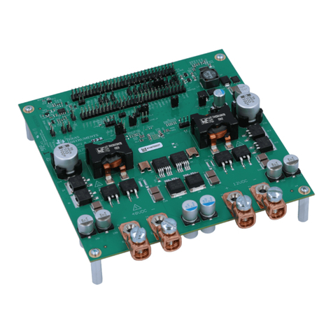
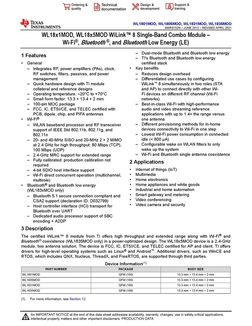
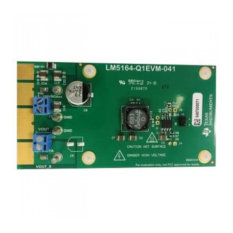
Texas Instruments TPS61280-585 User manual
Other Texas Instruments Control Unit manuals

Texas Instruments
Texas Instruments 2000 series User manual
Texas Instruments
Texas Instruments TPS23525EVM-815 User manual
Texas Instruments
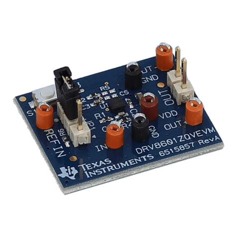
Texas Instruments DRV8601 User manual
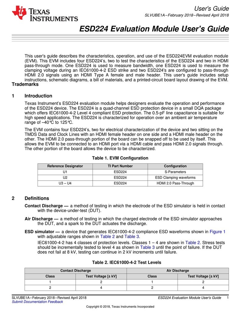
Texas Instruments
Texas Instruments ESD224 User manual
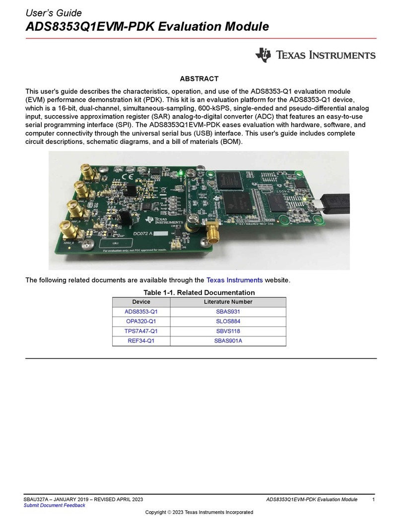
Texas Instruments
Texas Instruments ADS8353-Q1 User manual
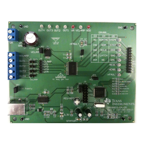
Texas Instruments
Texas Instruments DRV8803 User manual
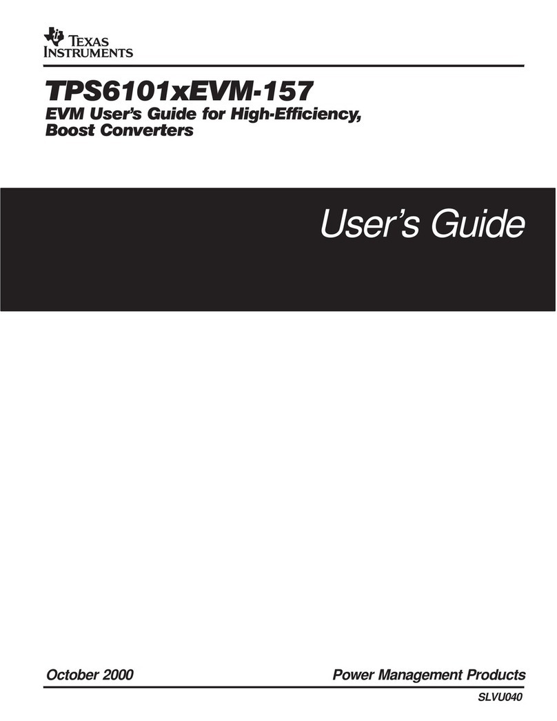
Texas Instruments
Texas Instruments TPS6101xEVM-157 User manual
Texas Instruments
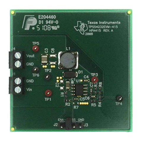
Texas Instruments TPS54232EVM-415 User manual
Texas Instruments
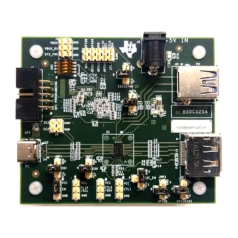
Texas Instruments TUSB564RNQ User manual
Texas Instruments
Texas Instruments TPSM84424EVM User manual

Texas Instruments
Texas Instruments bq26220EVM-001 User manual
Texas Instruments
Texas Instruments TPA3101D2 User manual
Texas Instruments
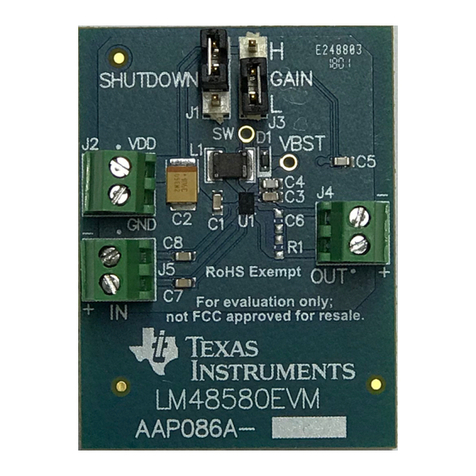
Texas Instruments LM48580 User manual
Texas Instruments
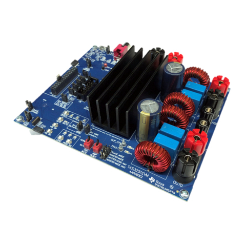
Texas Instruments TAS3251 User manual
Texas Instruments
Texas Instruments SimpleLink Wi-Fi BoosterPack CC3120 User manual
Texas Instruments
Texas Instruments LMP92066 User manual

Texas Instruments
Texas Instruments ADS1202 User manual
Texas Instruments
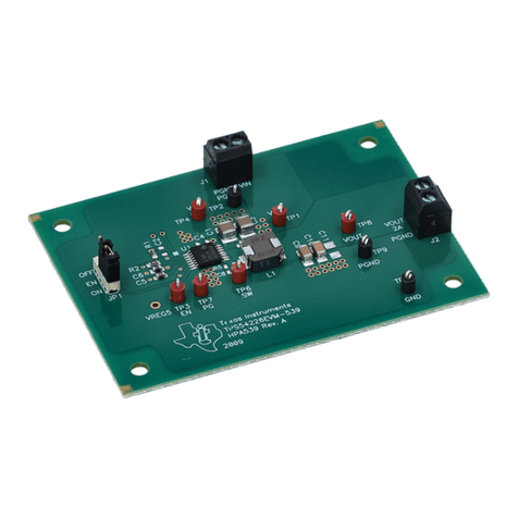
Texas Instruments TPS54226EVM-539 User manual
Texas Instruments
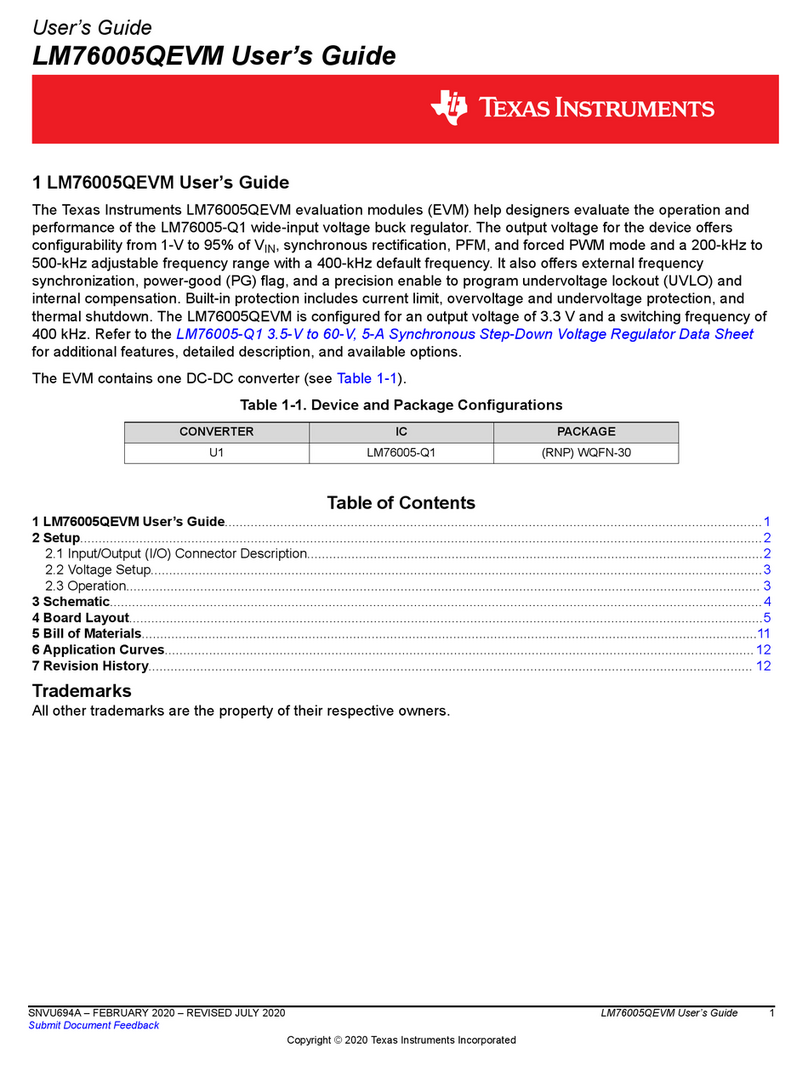
Texas Instruments LM76005QEVM User manual
Texas Instruments
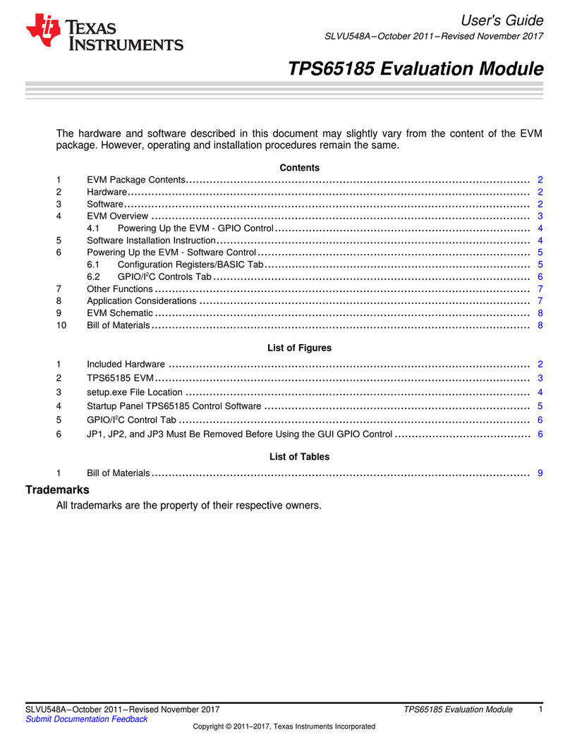
Texas Instruments TPS65185 User manual
Popular Control Unit manuals by other brands
Festo
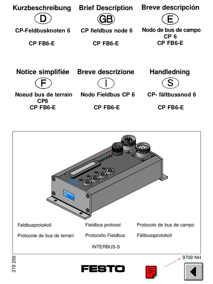
Festo Compact Performance CP-FB6-E Brief description
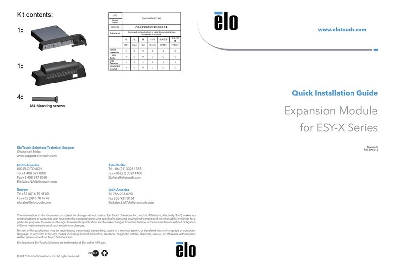
Elo TouchSystems
Elo TouchSystems DMS-SA19P-EXTME Quick installation guide
JS Automation
JS Automation MPC3034A user manual
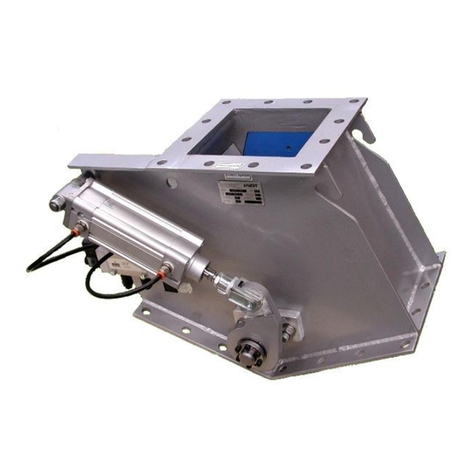
JAUDT
JAUDT SW GII 6406 Series Translation of the original operating instructions
Spektrum
Spektrum Air Module System manual

BOC Edwards
BOC Edwards Q Series instruction manual

KHADAS
KHADAS BT Magic quick start
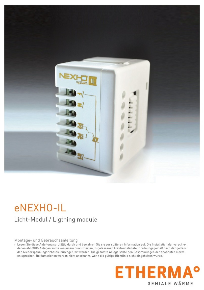
Etherma
Etherma eNEXHO-IL Assembly and operating instructions
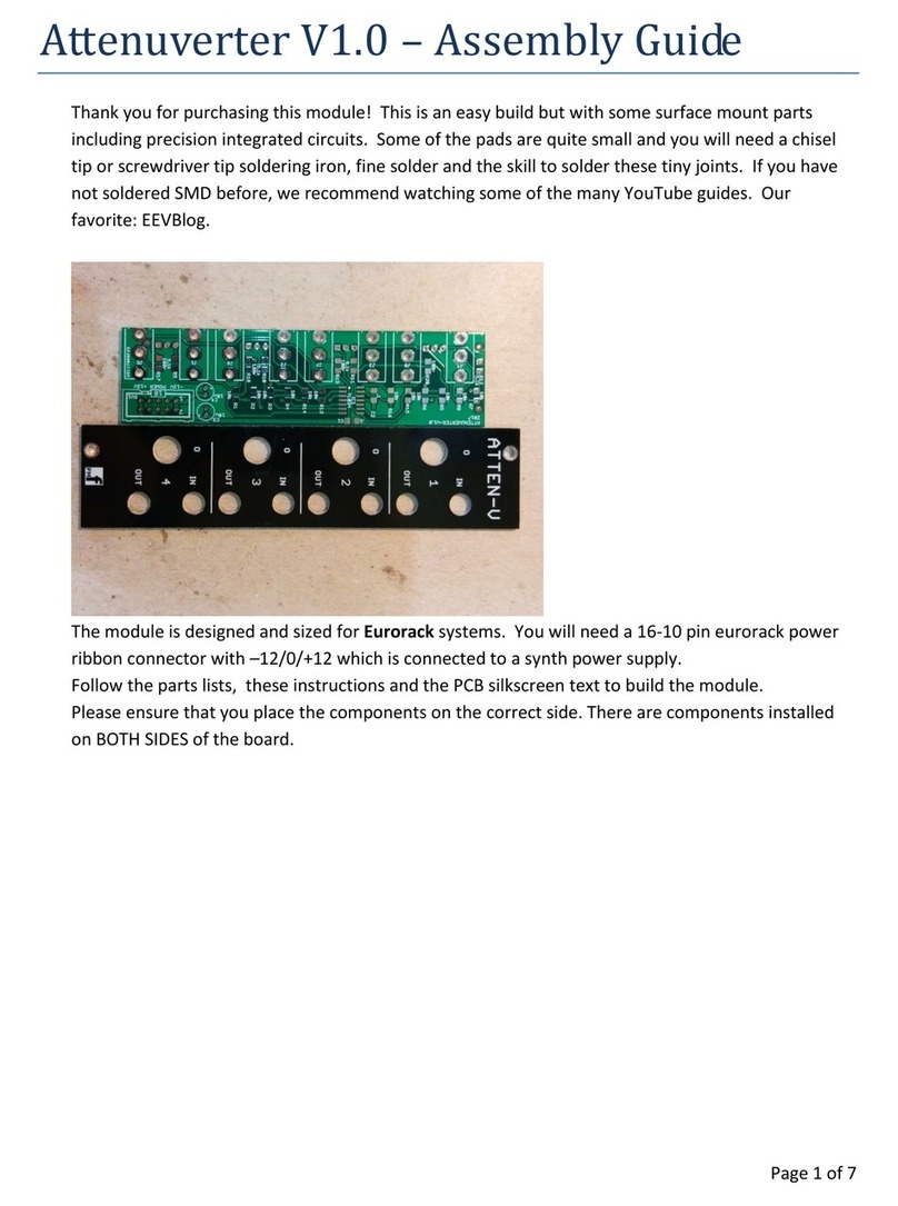
PMFoundations
PMFoundations Attenuverter Assembly guide
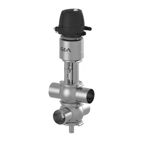
GEA
GEA VARIVENT Operating instruction
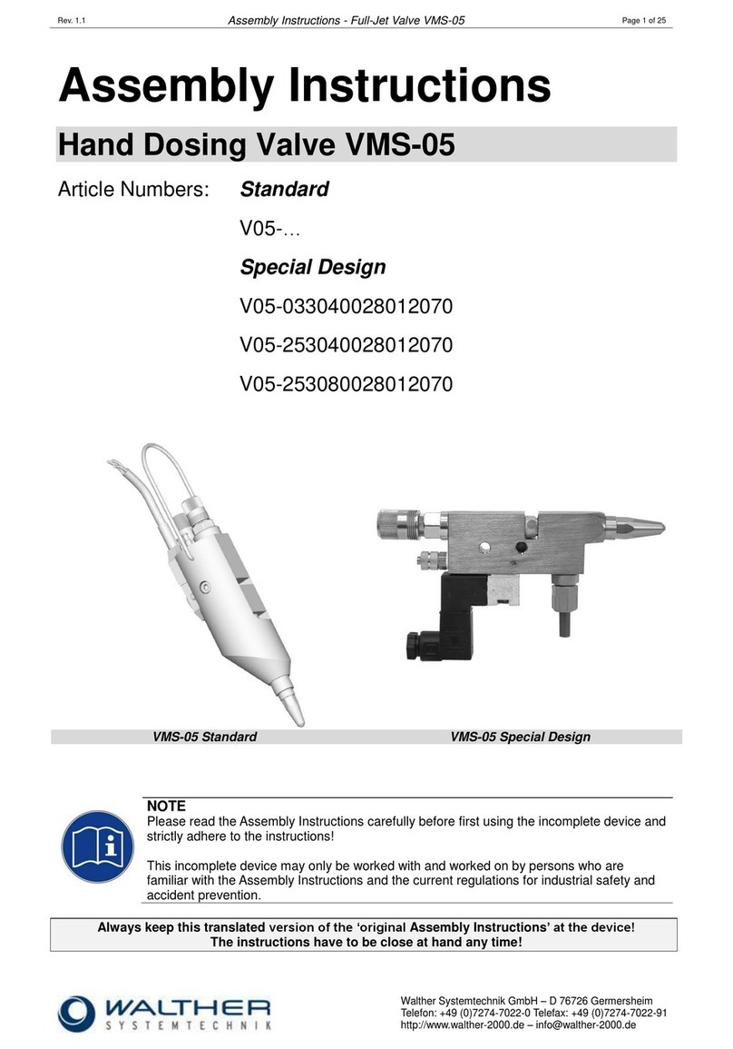
Walther Systemtechnik
Walther Systemtechnik VMS-05 Assembly instructions
Altronix
Altronix LINQ8PD Installation and programming manual
