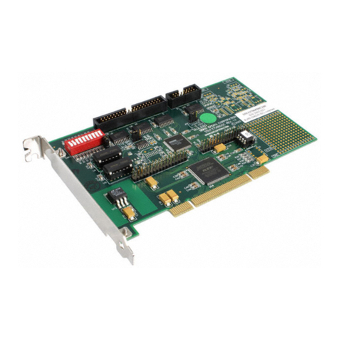
ADS5120EVM
SBAU078 3
www.ti.com
CIRCUIT DESCRIPTION
ANALOG INPUTS
The ADC receives differential inputs from eight transformers.
The eight single-ended inputs are provided via SMA connec-
tors J2, J3, J4, J5, J6, J7, J8, and J9. The inputs are AC-
coupled and have 50Ωtermination resistors.
External Reference Inputs
In addition to being able to use the internal reference of the
ADC, a reference circuit has been included on the EVM.
Using a precision +2.5V low-noise linear regulator as the
primary source, this circuit allows adjustment of the REFT
and REFB signals to the ADC using potentiometers R14 and
R16, respectively. A third source, CML, is also generated to
provide an adjustable common-mode voltage to be used by
the transformers during external reference operation. CML is
adjusted by potentiometer R28. In order to use the ADC with
external references, install jumpers W3 and W4, install jumper
W32 between pins 1 and 2 and jumper W22 between pins 2
and 3. If REFT is set to any voltage other than 1.32V, jumper
W22 should be installed between pins 1 and 2 for optimal
ADC performance. The ranges of the external reference
signals are shown in Table III.
Clock Inputs
The EVM provides separate clock inputs for the ADC (“ADC
Clock”) and the output buffer (“Output Clock”). This allows
the user to send a modified version of the ADC clock
(inverted, delayed, ect.) with the output data to generate the
required setup and hold times for the user’s interface.
An adjustment in the placement of the output clock that
captures the data relative to the ADC clock may be neccessary
depending on the specific timing requirements of the logic
analyzer used. If poor performance is observed, verify the
correct timing.
The ADC clock input is SMA connector J1 and has provisions
for serial and/or parallel termination. The buffered output
clock input is SMA connector J23. The clock inputs should be
50Ωsquare wave signals, +1.8V or +3.3V referenced to
ground (based on DRVDD voltage).
Control Inputs
The ADC has three discrete inputs to control the operation of
the device:
Standby
The ADC has individual standby control inputs for each of the
eight output data buses. These are controlled by the two dip
switches, S1 and S10. Table IV shows switch operation.
Duty-Cycle Adjust
With jumper SJP1 installed between pins 2 and 3, the
internal duty cycle adjust circuit is disabled. Installing SJP1
between 1 and 2 enables the internal duty cycle adjust
circuit. See device data sheet for details.
Output Enable
With jumper W1 installed between pins 1 and 2, the ADC
data outputs are enabled. The outputs are tri-stated with W1
between pins 2 and 3.
Output Buffer Enables
DIP switch S11 controls the ‘Enable’ function of the
SN74AVC16827 buffers for channels A, B, C, and D. DIP
switch S12 controls the ‘Enable’ function of the
SN74AVC16827 buffers for channels E, F, G, and H. With
the DIP switch set to the open position, the buffer outputs are
enabled. With the switches set to the closed position, the
outputs are tri-stated. Table V shows individual switch operation.
Power-Down Reference
With jumper W2 installed between pins 2 and 3, the ADC
internal reference is disabled and the device is in external
reference mode. The ADC is in internal reference mode with
jumper W2 installed between pins 1 and 2.
Power
Power is supplied to the EVM via banana jack sockets. A
separate connection is provided for a +1.8V analog supply
(J15 and J14), +1.8V digital supply (J18 and J19), +1.8/3.3V
digital driver supply (J21 and J22), and ±5V analog supply
(J16, J17, and J20).
TABLE III. Reference Voltage Adjustment Ranges.
MINIMUM TYPICAL MAXIMUM
SIGNAL VOLTAGE VOLTAGE VOLTAGE
REFT 0.9 1.32 1.6
REFB 0.3 0.781 0.9
CML 0.5 1.05 1.25
TABLE IV. Standby Switch Operation.
SWITCH SWITCH
SWITCH CHANNEL OPEN CLOSED
S1-1 H Operate Standby
S1-2 G Operate Standby
S1-3 F Operate Standby
S1-4 E Operate Standby
S10-1 D Operate Standby
S10-2 C Operate Standby
S10-3 B Operate Standby
S10-4 A Operate Standby
TABLE V. Output Buffer Switch Operation.
SWITCH SWITCH
SWITCH CHANNEL CLOSED OPEN
S11-1 A Tri-State Operate
S11-2 B Tri-State Operate
S11-3 C Tri-State Operate
S11-4 D Tri-State Operate
S12-1 E Tri-State Operate
S12-2 F Tri-State Operate
S12-3 G Tri-State Operate
S12-4 H Tri-State Operate
