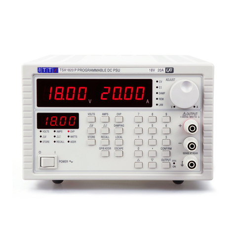
TTI TSX Series User manual

TSX Series
High Current Power Supplies
Service Manual
Book Part Number 48511-0240 - Issue 2

Table of Contents
General 2
Specification 3
Main Board Circuit Description 5
Overview 6
Mains Input, Switchmode and Linear Power Sections 6
Linear Regulator Control and supervisory Sections 9
Control Board Circuit Description (non-programmable versions only) 11
CPU Board Circuit Description (Programmable versions only) 13
Test & Calibration Procedure 15
Important Electrical Safety Considerations 15
Temporary Earthing for Primary Side Measurements 15
Order of Checks and Adjustments 15
Directions for Different Types 15
Test Equipment required for Recalibration only 15
Test Equipment for Main Pcb Testing 16
Repairs Following Power Fet Failure 16
Preparation for Main Pcb Testing 16
Preliminary Checks 16
Linear Regulator Checks 17
Testing Main PCB with LV on HF Switching Section 17
Testing of Main PCBs at Full Voltage 18
Recalibration of Assembled Power Supplies 19
Parts List 20
Manufacturing Changes 36
Circuit Diagrams 38
1

General
This manual has been prepared to aid the experienced engineer in the maintenance and repair of
this series of high current power supplies. For detailed operating information the user should
refer to the appropriate instruction manual.
Service Precautions
Recalibration or repair should only be attempted by skilled personnel in conjunction with high
quality test equipment. If the user is in any doubt as to his competence to carry out the work, the
supply should be returned to the manufacturer or their agent overseas for the work to be carried
out.
The tracks on the printed circuit boards are very fine and may lift if subjected to excessive heat.
Use only a miniature temperature-controlled soldering iron and remove all solder with solder wick
or suction before attempting to remove a component.
Safety
WARNING!
When the power supply is connected to the AC line, terminals may be live and the opening of
covers or removal of parts (except those to which access can be gained by hand) is likely to
expose live parts. The supply shall be disconnected from all voltage sources before it is opened
for any adjustment, replacement, maintenance or repair. Capacitors inside the supply may still be
charged even if the supply has been disconnected from all voltage sources, but will be safely
discharged about 10 minute after switching off power.
Any adjustment, maintenance and repair of the opened supply under voltage shall be avoided as
far as possible and, if inevitable, shall be carried out only by a skilled person who is aware of the
hazard involved.
Dismantling the Instrument
Observe the above safety warning before attempting to dismantle the power supply.
1. To remove the case upper, remove the 6 screws (3 each side) and lift off.
2. To remove the upper (CPU) pcb on programmable versions remove the 3 flat cables and the
2-way supply connector next to the regulator heatsink; note the orientation of the flat cables
(red stripe to pin 1). Remove the 2 RS232 and 2 GPIB screwjacks which secure the
connectors (and therefore the pcb) to the rear panel. Remove the 2 self-tap screws which
secure the pcb to the forward mounting pillars and lift it off.
3. To remove the main board disconnect the 2 leads to the output terminals from the M3 studs
at the front of pcb and unplug the nearby sense connections, noting the polarity of both.
Disconnect the flat cable from the control pcb (non-programmable versions only) and the 2
push-on connections at the rear of the pcb which feed the AC supply to the pcb from the
power ON-OFF switch. Remove the self-tap screws which secure the heatsink to the case
lower (1 for each heatsink). Remove the 9 screws which secure the main pcb support pillars
to the case lower (i.e. the screws accessible underneath the case lower) and lift the pcb
clear with its mounting pillars attached.
4. To remove the keyboard (programmable versions) or control board (non- programmable
versions) first remove the control knob (keyboard) by undoing the collet nut beneath the
knob cap or disconnect the output ON- OFF switch (control board) from the pcb. Remove
the screws which secure the board to the front panel and lift free.
5. Reassemble in the reverse order. Take great care to ensure that the connections to the
output terminals (front and rear) are exactly as found before dismantling and that no
insulation creepage and clearance distances have been compromised. Ensure that the foil
screen over the output wires in the case lower is properly earthed via the appropriate pcb
support pillar.
2

Specification
Output Specifications
Operating modes: Constant voltage or constant current with automatic crossover.
Voltage Range: 0V to 35.3V (35V/10A), 0V to 18.15V (18V/20A)
Current Range: 0.01A to 10.2A (35V/10A), 0.01A to 20.2A (18V/20A)
Overvoltage protection range: 1V to 40V (35V/10A), 1V to 25V (18V/20A)
Setting Resolution: 10mV, 10mA
Load Regulation: <0.01% for a 90% load change
Line Regulation: <0.01% for a 10% line voltage change
Output Impedance: <1mΩin constant voltage mode,
>5kΩin constant current mode
Ripple and noise: <3mA RMS typical in constant current
HF Common mode noise: Typically <3mV RMS, <10mV pk.
Transient load response: <200us to within 50mV of set level for a 90% load change.
Temperature coefficient: Typically <100ppm/oC
Overvoltage protection delay: <200us
Protection functions: Overvoltage trip
Regulator overtemperature: Sense miswiring
Status indication: Output on/off LED
Constant voltage mode LED
Constant current mode LED
Trip message
Output switch: Electronic
Output terminals: 4mm output terminals at front
Screw terminals for output and sense at rear
Input Specifications
Input voltage range: 180V to 270V RMS
90V to 135V RMS
Power requirement: 47 to 63Hz, 600VA max.
Voltage range selection: Rear panel slide switch
Meter Specifications
Meter types: Separate 4-digit meters for voltage and current with 12.5mm (0.5")
LED displays
Meter resolutions: 10mV, 10mA
Meter accuracies: Voltage 0.2% ± 1 digit, Current 0.5% ± 1 digit
Front Panel Controls
Voltage setting: Direct keyboard entry or quasi-analogue rotary control
Current setting: Direct keyboard entry or quasi-analogue rotary control
Overvoltage setting: Direct keyboard entry
Output on/off: Push button with dual indicator LEDs
3

Note: All voltage and current levels set via the keyboard are displayed on a separate 0.0.3" 4-
digit display. This entry preview system ensures that the user can observe the value entered
before it is effected thus avoiding possible error. The display is also used for setting additional
functions. When the output switch is on and no other function is selected, the display shows
output power in Watts.
Additional keyboard functions
Increase or decrease voltage or current in user-selectable steps (delta mode). Store and recall
voltage, current and OVP levels from non-volatile memory (25 memories). Set digital interface
type (RS232 or GPIB), set baud rate, set address.
Digital Interfaces
Operational functions: Set voltage; set current; set OVP; set output on/off; read output
voltage; read output current; read output power.
RS232: Variable baud rate, 9600 baud maximum. 9 pin D-connector
(female). Fully compatible with ARC (Addressable RS232 Chain)
system.
GPIB: Conforming with IEEE488.1 and IEEE488.2
Output Specifications – Remote Operation
Output Voltage Setting: 12 bit resolution (10mV steps)
Output Current Setting: 12 bit resolution (10mA steps)
Setting Accuracy: Voltage: + (0.1% + 10mV), Current: + (0.2% + 20mA)
Output Switch: Electronic by interface command
Readback Resolution: Voltage: 10mV over the entire range
Current: 10mA over the entire range
Readback Accuracy: Voltage: + (0.2% of reading + 1 digit)
Current: + (0.5% of reading + 1 digit)
Response Time Over RS232/GPIB
Interface: <15ms (single command, buffer empty)
Power Supply:
A
n internal time constant, T, (typically 22ms) governs the settling tim
e
of a step voltage increase. Settling time to within 1% of the step
change = 4.6T, to 0.1% = 6.9T, to 0.01% = .2T; for example, after a
10V step the output will be within 1 digit (10mV = 0.1%) of its new
value in typically 150ms. For load currents of 1 Amp or more, settling
times for downward steps will be very similar; however, response
times will be longer at low loads.
General
Electrical safety: Built to comply with IEC 348
Temperature specifications: 5oC to 40oC operating, 20% to 80% RH
–40oC to 70oC storage
Size: 200 x 140 x 350mm (WxHxD) half rack width x 3U height (optional
rack mounting kit available)
Weight: 5.5kg
4

5

Main Board Circuit Description
Overview
The main board comprises a mains driven HF switchmode DC-DC isolating convertor using pulse
width modulation (PWM) which feeds a linear regulator operating at low input-output voltage
difference as shown in the skeleton circuit diagram opposite.
Mains Input, Switchmode and Linear Power Sections
Component references are to sheet 1 of the circuit diagram unless stated.
Mains Input Components and Fusing - When the power supplies are used on 240V, fused plug
tops should be fitted with a 5A fuse. The mains supply enters at the IEC receptacle on the rear
panel and is wired, via the front panel mains on-off double pole switch, to Faston connectors on
the main PCB. A 10A PCB mounted fuse F1 limits damage on switchmode failure. Varistor VDR1
clips mains 'spike' voltages for component protection. R212 provides safety discharge for C1,C2.
Input Noise Filter - Double wound filter choke L1, X capacitors C1,C2 and Y capacitor C4
provide low pass HF filtering to minimise noise currents injected into the mains supply by the
switchmode section. Y capacitor C4 also provides a low impedance HF path from the switchmode
section to case/earth.
Mains Voltage Selection - Voltage selector SW2 connects BR3 and series connected reservoirs
C9,C10 for bridge/voltage doubler rectification and the two 120V primary sections of 50 Hz
auxiliary transformer T1 in series/parallel in its 230/115V positions respectively. Rectified voltage
is 200-380 VDC. R5,R6 ensure voltage sharing and provide a safety discharge path for C8,C9.
C3,C7,C8 minimise rectifier snap-off transients and HF noise.
Mains Inrush Control - At switch on triac TC1 blocks and reservoirs C9,C10 charge up slowly
via the 33Ωof cold thermistor PTC1; this action also causes the primary peak voltage across
auxiliary transformer T1 and the inrush control voltage across C6, derived from a T1 primary tap,
to increase slowly. When the latter reaches about 8V enough current flows through R3,D10,R92
to trigger latch Q5,Q6 on, providing continuous drive to TC1 gate. D15 inhibits triggering during
BR3 conduction to avoid sudden connection of rectified mains voltage to reservoirs C9,C10.
Once turned on TC1 remains conductive until AC supply ceases or falls to a very low level
unlatching Q5,Q6. If TC1 fails to turn on, thermistor PTC1 switches into a high resistance state
within a few seconds, protecting itself against overtemperature and disabling the power supply.
HF Power Switching Stage HV power FETs Q1,Q2 form a totem pole switch that switches the
primary of the ferrite HF power transformer T2 to HV DC rails VRECT+ or VRECT- during on
periods and presents an open circuit during the off period of the PWM waveform. C11,C12 allow
the return end of the primary winding to assume about mid-rail voltage and provide low
impedance HF returns to either rail for the primary current. Snubber C13,R7 absorbs most of the
spike energy stored in the leakage inductance of T2 at FET switch off. T2 primary is returned via
current transformer T4. Plug PJ4 allows disconnection of Q1,Q2 from the HV rail during testing.
Switchmode auxiliary supply - Stabilised +12V at 50 mA for the PWM driving circuits is derived
from a primary side auxiliary winding on T1 via BR1,C25,IC2. PWM switching controller IC1
incorporates undervoltage lockout which inhibits operation until VCC reaches about 9V.
PWM Generation - The oscillator of PWM controller IC1 runs at about 160 kHz for 80 kHz PWM
output and generates a master saw- tooth waveform across timing capacitor C19 swinging
between about +0.9 and +2.8V. Minimum PWM deadtime of approximately 680 nsec corresponds
to the reset (negative going) stroke of this waveform. The PWM on pulse starts at the beginning
of the upward ramp and is terminated when the ramp voltage rises to about 1.25V below the DC
level at the error amplifier output COMP. Ramp charging current into C19 is proportional to the
current drawn from pin RT and is set by R14 for the main part of the PWM on time. The positive
pulse from IC1 CLK output turns on Q30 via C49,R49 discharging C50 during ramp reset. When
the upward ramp starts, C50 recharges rapidly through R47 momentarily increasing C19 charging
current and ramp slope over the first 300 nsec or so of the on period. This arrangement allows
stable generation of very narrow on pulse widths required at very low output voltages.
6

HF Switch Drive - IC1 PWM outputs A and B are applied via driver IC11 to each end of drive
transformer T3 primary, providing alternating antiphase PWM outputs of about 12V peak from
each secondary. Gate resistors R18,R22 slow Q1,Q2 switching transitions to about 100nsec to
limit RFI generation. R9,C14 and R10,C15 minimise drive waveform overshoot and cross
conduction of Q1,Q2. Schottkys D8,D9 avoid IC11 substrate reversal.
Soft Start - If IC1 detects VCC undervoltage, PWM generation is inhibited and soft start capacitor
C18 discharged. When VCC is adequate and PWM generation is enabled IC1 charges C18
slowly. The PWM on pulse width is internally limited by the voltage on C18. As C18 charges
narrow PWM pulses appear at about +1.25V which widen steadily until IC1 error amplifier takes
control. This feature allows orderly start up of the switchmode section after switch on.
Dual Function Opto-coupled Control - OPTO1 provides both analogue feedback for PWM
control and digital shut down control across the isolation boundary to the switchmode section. In
normal operation OPTO1 input current drive is arranged to ensure a minimum output current of
about 40 microamps. When switchmode shutdown is required the Supervisory System described
later cuts off OPTO1 input turning off Q13, inhibiting PWM output via D7,R157,Q3,Q7 and
clearing soft start capacitor C18.
PWM Control - OPTO1 collector feeds the error amplifier of IC1 (output at COMP) which is
operated in virtual earth mode to maximise optocoupler bandwidth. Clamp Q20 improves
amplifier overload behaviour. PWM output pulses cease at OPTO1 minimum current level.
Switchmode Protection - T2 primary current is returned via current transformer T4 primary.
Virtually instantaneous protection against gross overcurrents following severe faults is effected
when T4 secondary output rectified by D21,D22 generates enough voltage across R156 to turn
on Q3,Q7 regeneratively via spike filter R121,C68. PWM output is immediately inhibited and soft
start capacitor C18 discharged. If the cause of overcurrent persists the process will repeat
(hiccough) after the subsequent soft restart. The limiting of peak operational current levels is
described later under Switchmode Current Limiting. If switchmode heatsink SK1 temperature
exceeds about 100 deg C thermostat TS1 opens triggering latch Q3,Q7 on via Q13,D7,R157.
This condition is registered elsewhere by supervisory logic to avoid automatic restart after
cooling.
HF Rectification and Filtering - The centre tapped secondary of T2 feeds ultra fast epitaxial
dual rectifier diode D14 which delivers rectified or freewheel current to HF power choke L3.
R75,C65 and R66,C64 reduce diode reverse recovery voltage spikes. Ferrite choke L3 and
reservoirs C73,(C74),C33 form a low pass choke input filter delivering low ripple DC output
voltage proportional to pulse width. R55 provides the minimum loading necessary for control over
the full 38 to 1.5 VDC output range.
Series Regulator Power Elements - Parallelled plastic cased bipolar power transistors are used.
35V/10A supplies use two devices sharing the single secondary side heat sink with rectifier D14
and driver transistor Q4 while 18V/20A supplies use four devices mounted on a separate
heatsink. Emitter resistors (R38-R41 as appropriate) ensure current sharing. Device dissipation is
minimised by using the switchmode section to regulate the collector-emitter voltage at about 1.5V.
Driver transistor Q4 is mounted on the same heatsink as D14. To avoid the premature driver
collector saturation of the Darlington connection, Q4 collector voltage is maintained about 3V
above the output transistor collectors by a floating auxiliary supply. R44,Q29 limit driver current to
about 2A. Voltage and current error amplifier outputs are applied to the driver via predriver
circuitry D11,D12,R34,Q8,R12. Driving ENABLE low shuts down the linear regulator.
7

Auxiliary Supplies - Several control auxiliary supplies are derived from 50/60 Hz auxiliary
transformer T1 secondaries:
(i) +5V 270mA DC via BR2,C27,IC4 for linear control, ADC, (DACs) and drive for the two
meter LED displays.
(ii) –5V 50mA DC via D2,C28,IC3 for linear control, ADC (and DACs).
(iii) 3V 1.5A DC floating, unstabilised via D18,D42,D26 for driver Q4 collector.
(iv) 10V 0.9A AC via PJ2 for the CPU board.
(v) 12V DC via BR1, C25 and IC2, supplies IC1, IC11 and Q20.
Only programmable versions incorporate CPU board and DACs. Reference diodes D35 and D36
provide +2.45V and -2.45V reference voltages respectively. R80 bleeds current from +5V to the
negative output terminal to provide a small output current sink capability.
Inadequate auxiliary control supplies are detected by positive and negative voltage detectors
R42,D51,R48,Q23 and R43,R50,Q23 respectively via on delay Q21,C48,IC12-B. Status lines
AVAUXT and AVAUXT bar go high and low respectively only when IC4 input, IC4 output and IC3
output voltage have maintained about +7, +4 and -3.5 VDC respectively for about 150 msec.
Linear Regulator Collector Voltage Control System - Virtual earth error amplifier IC6-B current
drives OPTO1 input via D49,Q24 so as to maintain low collector-emitter voltage across the linear
regulator power transistors. At zero collector current the collector voltage sets to about +1.85V
determined by the -5V supply and R127,R136. At higher currents increasing voltage drops across
emitter sharing and current sense R54 resistors and, in 35V/10A supplies current feed-forward
via R126, give a linear reduction in collector- emitter voltage to about 1.2V at the maximum output
current of 5A per device. This arrangement provides increased Vce "headroom" at low output
currents to accommodate the larger transient dip in switchmode output voltage that follows
maximum current demand without increasing maximum dissipation. R129,R130,R11,C38 assist
stability while D31,D39,Q28 speed amplifier overload recovery. R128 is selected to normalise
control loop gain.
Switchmode Shutdown Control - In normal operation ENABLE and ENABLE bar are high and
low respectively. Even if IC6-B output goes transiently negative, reverse biassing D49, OPTO1
input is still maintained at about 300 microamps by R133,Q24; low enough for PWM output to
cease although Q13 in the switchmode section remains on and IC1 active.
The switchmode section is shut down by driving ENABLE and ENABLE bar low and high
respectively; turning off Q24 and driving OPTO1 input and output currents to zero. Q13 in the
switchmode section then turns off inhibiting PWM output and holding soft start capacitor C18
discharged. IC6-B output is also driven negative via D62 to avoid switchmode surging on re-
enablement.
Switchmode Maximum Current Limiting - The maximum current demanded from the
switchmode section will be the sum of the maximum DC output current and the maximum
transient current required to charge switchmode filter capacitor(s) C73,(C74). The former is
limited to 10/20A, depending on the model while the latter is proportional to the maximum positive
rate of change of switchmode output voltage.
Diode D30 limits the current from IC6-B input via R132 to about 2 microamps. This is balanced by
the current from feedback capacitor C39 limiting the rate of increase of power transistor collector
voltage to about +1.3 V/msec, corresponding to a peak current into the filter capacitors of about
1.3/6.3A in the 35V/10A and 18V/20A units respectively provided the output voltage remains
constant.
Protection outside constant voltage output mode is provided by circuitry around Q19. If the rate of
change of output voltage approaches about +6/+3V per sec for 35V/10A and 18V/20A units
respectively differentiating network C52,R124 begins to turn off Q19 injecting current into the
amplifier input via R123,D17 to limit the switchmode section output. This mechanism protects
even against the unlimited rate of rise of output voltage following connection of batteries to the
output terminals.
8

Linear Regulator Control and supervisory Sections
Component references are to sheet 2 of the circuit diagram unless stated. Note that 0V and the
returns for the +5V and -5V auxiliary supplies for this circuitry are effectively at the positive
output terminal potential of the power supply.
Voltage Control Amplifiers - When the output is switched on CMOS analogue selector IC7-A
applies the voltage programme voltage at PJ1-19 to the input of noninverting buffer amplifier IC5-
C and amplifier input current is removed via R74,IC7-C in non-programmable versions. Presets
VR3,VR2 remove control loop offset and trim programme gain respectively. The buffered output
is applied to the differential input voltage error amplifier around IC5-A. Preset VR1 is adjusted for
maximum output-sense voltage rejection. Capacitors C41,C42 minimise noise and are matched.
R70,R71,C36,C46 assist loop stability. D23-26 and feedback clamp D40,R77,R78 limit IC5-A
input and output excursions and speed amplifier recovery. IC5-A controls the output via D11.
Current Control Amplifier - The current limit programme voltage at PJ1-20 is attenuated by
VR6,R81,R79,R208. When output is switched on CMOS analogue selector IC7-B applies
attenuated programme voltage from R79/R208 to the non- inverting input of current error amplifier
IC5-D. The voltage across the sense terminals of the four terminal output current sense resistor
R54 is applied to IC5-D inverting input via R87,R115. At current limit IC5-D takes over output
control via D12. Presets VR8 and VR6,VR9 remove control loop offset and trim maximum
indicated and output current respectively. Network R56,R84,R88 compensates for output sink
current removed via R80.
Output Off Control - Output on-off control is entirely electronic and exercised by OPCTL from
the front panel output switch (or CPU board in programmable versions) via debounce C35,R26.
When output is switched off OPON goes low so that CMOS analogue selector IC7-A applies a
low negative voltage from R72,R73 to IC5-C input setting the supply output to about -200mV
while selector IC7-B applies a low positive voltage from R82,R83 to IC5-D input setting the
output current limit to about 50mA.
Constant Voltage/Current Status Detection - Transistor detector circuits Q25,R148,R149,R152
and Q26,R150,R151,R153 detect whether the output of the voltage or current error amplifier is
controlling the output of the power supply and provide corresponding digital outputs from PJ1-29
and PJ1-30 to the metering/CPU boards.
Over Voltage Detection - The output of attenuating differential amplifier IC5- B is proportional to
the output sense voltage. When this exceeds the OVP programme voltage applied to PJ1-18
amplifier IC6-A output goes high. During shut down OVP detection is inhibited via D32.
Supervisory Fault Latch - IC9-B,IC8-D, IC12-D form a master fault latch which can be tripped
(set), driving IC9-B low and disabling switchmode and linear regulators via IC9-A, by a variety of
faults detected by the surrounding circuitry:
(i) Activation of over voltage (OVP) detector/comparator IC5-B/IC6-A for about 200 usecs
(C70,R139,IC12-A).
(ii) Opening of thermostat TS2/TS3 on 35V/10A or 18V/20A respectively, on overheating of
secondary side heatsink SK2/SK3 via IC8-B.
(iii) If no switchmode output pulses are detected by pulse detector R45,C37,Q27,D60 for
about 20 secs (C69,R140,IC8-B) due to TS1 opening on primary side heatsink
overtemperature.
(iv) Transistors detectors Q16,R202,R203 or Q17,R204,R205 turning on due to excessive
load-sense terminal podential differences for about 350 usecs (C71,R147,IC9-B) on
miswiring of load or sense terminals.
The TRIPPED output at PJ1-28 goes high on tripping of the fault latch. The fault latch is reset at
switch on via LED1,R27 or while reset line CPU RUN is driven low in programmable versions.
9

System Shutdown - Shutdown of both switchmode and linear regulators is asserted via IC9-A of
the supervisory logic following power up, detection of inadequate auxiliary supplies, tripping of the
master fault latch or, in programmable versions, during CPU board driven resetting of that latch.
Output Circuit Components - C16 and C34 assist linear regulator stability. D37 protects against
reverse polarity connection of external batteries or other power supplies to the output. Coaxial
toroidal choke L4 and front panel mounted ceramic capacitors CA,CB,CC form a lowpass HF filter
attenuating common mode and differential noise generated within the power supply.
R57,58 maintain a working connection between output and sense terminals if the latter are left
disconnected. R96,C51 and R97,C53 assist stability when remote sensing is used.
Voltage and Current Metering Points - Chain R17,R59,VR4,R211 attenuates the voltage sense
p.d. to feed the multiplexed differential input ADC on the control/CPU board from PJ1-2 and PJ1-
4. The current signal is taken directly from the current sense network to feed the ADC from PJ1-5
and PJ1-3.
10

Control Board Circuit Description
(non-programmable versions only)
The control pcb contains the voltage and current measurement system, the display, the controls
for adjustment of the output voltage, current limit and over voltage protection, plus the output
on/off switch connection. The pcb is connected to the main pcb by a 34-way flat cable. The
control board also contains three preset adjustments.
The measurement system and display are controlled by a microcontroller IC1.
The measurement of output and preset values of voltage, current and OVP is performed by the
12 bit analog to digital converter IC2. The measurement rate is controlled by the 4.0MHz ceramic
resonator XL1 connected between pins 22 and 23 and the buffered version of this 4MHz signal at
pin 25 is used as the clock to the microcontroller IC1. The ADC, IC2, is a dual slope converter
and provides just over 8 readings per second when clocked at 4MHz. The ADC is run in
continuous mode and the status signal on pin 2 is read by the microcontroller every 6ms. When a
reading is ready the microcontroller reads the 12 bit binary value and then converts it to 7
segment BCD and stores it ready to be sent to the display. After each reading the microcontroller
switches the input multiplexers IC3 and IC4 to the next required input. In this way it is possible to
read and display any of the following:
Preset Volts
Preset Current
OVP
Output Volts
Output Current
The multiplexers are controlled by the latch, IC6, which also drives the additional indicator LEDs,
this latch is driven by the microcontroller. The decision on what to measure and display at any
time is taken by the microcontroller and in order to do this correctly a number of status signals
and switches are monitored on a regular basis. These are:
VLIMD from the main board
ILIMD from the main board
TRIPPED from the main board
PRKEY the preset key signal
OVPKEY the OVP key signal
DAMPING the DMPGKEY signal
OPON the output on/off switch signal
all these signals may be read by the microcontroller as required.
The +2.45V reference line VREF+ is derived from reference diode D35 on the main PCB,
attenuated to about 188 mV by divider R206,207 and then connected to the control board as
ADREF via PJ1-17. It is then applied to the reference input of analogue to digital converter IC2,
yielding a sensitivity of about 92 uV per digit.
The set current signal ISET is taken from the VR4 wiper to feed the current control amplifier on
the main PCB via PJ1-20; it is also fed to the ADC system via adjustable attenuating chain
VR7,R34-36 for display of preset voltage level.
The voltage control signal VSET is derived from the wipers of the coarse and fine voltage controls
VR1 and VR2 via weighting network R19,20 to feed the voltage control amplifier on the main PCB
via PJ1-19; it is also fed to the ADC input via adjustable attenuating chain VR6,R26,28,33 for
display of preset voltage level.
11

The over voltage protection user preset potentiometer VR3 is fed from the same +2.45V
reference voltage as the other controls but connected from the main PCB via PJ1-15 as
OVPREF+. The OVP set from VR3 wiper OVPSET is fed to the OVP trip comparator IC6-A on the
main board via PJ1-18; it is also fed to the ADC input via divider R37,41 for display of preset over
voltage trip level.
The output on-off switch connected at SW1 drives the output off-on control line OPON bar
providing off-on control at the main PCB via PJ1-33.
The two 4-digit LED displays are driven by IC1 via the segment latch IC10 and the digit latch IC7.
Digit current is provided by IC8 and individual segment current is limited to 50mA by the resistors
R1 to R8. The digit multiplex rate is 2ms and is controlled by IC1 which also provides the inter
digit blanking to prevent ghosting segments.
The power supply for all the above circuitry is provided by the main board.
12

CPU Board Circuit Description
(Programmable versions only)
Overview
The power supplies use a Z80 microprocessor to accept and process commands (from the
keyboard, RS232 interface or GPIB interface) and to pass on the necessary command and
control information to a microcontroller, located on the other side of an opto-isolated interface,
which controls the setting of the values for voltage, current and OVP and the measurement of
output voltage and current. The opto isolated interface is later referred to as the Inter-
Processor-Interface or IPI.
The CPU board contains the Z80 microprocessor, program memory, data memory, RS232
interface, GPIB interface, keyboard scan circuitry and the interface to communicate with the
microcontroller. The microcontroller is also on the CPU board together with its display control
latches and drivers and the analog to digital converter which measures the output voltage and
current. The Z80 and microcontroller are electrically isolated from each other by an opto-coupled
interface. This allows the Z80 and its interfaces to operate at mains ground potential while the
microcontroller and the output of the power supply may be up to 300 Volts away from ground. The
circuitry on each side of the isolation interface is described below.
The Z80 uses a 4 digit LED display and 16 LEDS to communicate status information to the user,
The microcontroller uses two 4 digit LED displays to show voltage and current values at the
output. All LED displays are mounted on the keyboard pcb, see next section.
Z80 Circuit
The 4.9152MHz clock for the Z80 is generated by IC13 which also provides the 1.6ms clock used
as the NMI signal, the various clocks used to specify the RS232 interface baud rate and the
600Hz buzzer drive. The 1.6ms clock is used by the CPU as follows. Six ticks are used to
generate the LED display and the 16 status LEDs. The seventh tick is used to read the
continuously rotating pot and alternately to scan the keyboard and to generate timing delays for
the slower parts of the system or to update the system status.
The memory map is divided into a 56k byte area at IC10, which contains the system code in
ROM, and an 8k byte area at IC11 containing RAM which is battery backed and holds all the
system parameters and power supply stores. IC10 is mapped in the address range 0000H to
DFFFH (56k bytes) and IC11 is mapped in the address range E000H to FFFFH.
The input/output devices are selected by IC14 during IORQ cycles. Each output from IC14
selects a range of 8 ports as follows
00H to 07H RS232 serial device IC5.
08H to 0FH 7210 GPIB controller IC3.
10H to 17H Segment latch. Drives the LED display segment lines and scans the keyboard
rows.
18H to 1FH Digit latch. Drives the LED display digit lines. Also controls the buzzer and NMI
enable signals.
20H to 27H Status read. Reads from keyboard columns, the pot adc and the IPI.
28H to 2FH Control port. Writes to the IPI, sets the baud rate and controls the pot adc.
When the power fail line (PF bar on PJ1 pin 5) goes low the system immediately enters a reset
condition by Q6 turning on and discharging C2. This causes the reset lines, MRST and MRST
bar, to assume their active states and all circuitry is held in the reset condition. The ram, IC11 is
switched to battery power and disabled by pulling the chip select input high via the RAMSAVE
line thus ensuring that the contents are retained until power is restored.
13

Microcontroller Circuit
This section contains the voltage and current measurement system, the display drivers and the
DACs which are used to set the output voltage, current limit and over voltage protection.
The measurement system and display is controlled by a microcontroller IC26.
The two 4-digit LED displays on the front panel board are driven by IC26 via the segment latch
IC30 and the digit latch IC31. Digit current is provided by I32. The digit multiplex rate is 2ms and
is controlled by IC30 which also provides the inter digit blanking to prevent ghosting segments.
The measurement of output and preset values of voltage, current and OVP is performed by the
12 bit analog to digital converter IC27. The measurement rate is controlled by the 4.0MHz
ceramic resonator XL2 connected between pins 22 and 23 and the buffered version of this 4MHz
signal at pin 25 is used as the clock to the microcontroller IC26. The ADC, IC27, is a dual slope
converter and provides a little over 8 readings per second when clocked at 4MHz. The ADC is run
in continuous mode and the status signal on pin 2 is read by the microcontroller every 6ms. When
a reading is ready the microcontroller reads the 12 bit binary value and then converts it to 7
segment BCD and stores it ready to be sent to the display. After each reading the microcontroller
switches the input multiplexer IC28 to the next required input. In this way it is possible to read and
display output volts and output current
The multiplexer is controlled by the latch, IC29, which also drives the additional indicator LEDs
CV and CI and some of the control lines to the DACs. This latch is driven by the microcontroller
The decision on what to measure and/or display at any time is taken by the microcontroller and in
order to do this correctly a number of status signals are monitored on a regular basis. These are:
VLIMD from the main board
ILIMD from the main board
TRIPPED from the main board
These signals are read by the microcontroller from the output circuitry of the instrument and are
combined with commands from the Z80 via the IPI to determine what appears on the two 4 digit
displays. In this way it is possible to show preset voltage, preset current, output voltage and
output current.
The power supply for the microcontroller circuitry is provided by the main board.
Keyboard Circuit Descpription (Programmable Versions only)
The front panel pcb contains the key matrix, 16 indicator LED's and the 4 digit LED display which
are controlled by the Z80,and the two 4 digit LED displays and 2 indicator LEDs which are
controlled by the microcontroller.
The key matrix is scanned every 22ms by the Z80. All key coding, de-bounce and key repeat
operations are controlled by the software. The 4 digit LED display is multiplexed along with the 16
LEDs, which are treated as 2 extra digits, at a rate of 1.6ms per digit. The Z80 also provides the
inter digit blanking to prevent ghosting segments.
The continuously rotating pot, VR1, is connected to an 8 bit analog to digital converter, IC2, via a
pair of analog gates in IC1. This allows the Z80 to select the required track of the pot from which
to establish a pot rotational movement value. This is done by reading the adc every 22ms and
calculating the difference in software.
The two 4-digit LED displays are driven by the microcontroller at a digit multiplex rate of 2ms. The
microcontroller also provides the inter digit blanking to prevent ghosting segments.
14

Test & Calibration Procedure
Important Electrical Safety Considerations
A substantial proportion of the power supply main PCB is occupied by primary side circuitry
comprising tracks, terminals and components (including one of the large heat sinks) which
normally operate at AC mains potential.
The incoming AC supply to the PCB or PSU under test must be isolated by means of a 1:1
isolation transformer of at least 700VA rating for safety and noise control.
High voltages (up to 400V peak) are always present in the primary side circuitry. Note that
removing bridging connector PJ4 disconnects HV only from the power FETs.
Components at high voltage lie within a well defined area of the main PCB which includes the
large heat sink SK1. The operator should familiarise himself with the boundaries of this area and
avoid contact within it.
Primary side earthing - Earthing of the Y filter capacitor at GND3, at the hex spacer, is desirable
to control noise effects.
HV Capacitor Discharging - Allow 6 mins for HV reservoirs C9,10 to discharge from 400V to
40V via R5,6. Alternatively discharge both capacitors with 100R 5W resistor.
Temporary Earthing for Primary Side Measurements
Voltage checks and CRO measurements on the main PCB primary side circuit are only carried
out with 60 VDC maximum applied to the switching power FETs. Primary side node VRECT-
must be well grounded (e.g. at Q1,2 mount bolts) to protect the user and the external PSU during
these measurements. Not that this negates the protection normally provided by the isolation
transformer and earths the particularly easily touched heat sink SK1.
Order of Checks and Adjustments
The power supplies comprise a switchmode pre-regulator operating at mains (primary) potential
which feeds a (secondary) linear regulator. The latter must be working properly for proper
operation or testing of the former. Both regulators obtain their auxiliary supplies from 50Hz
auxiliary transformer T1 the primary of which is fed from the mains potential (primary) section of
the PCB which is therefore energised during all tests. The order of checks and adjustments
reflects these dependencies and should be followed after any repair work.
Directions for Different Types
The directions are written as far as possible to cover normal (non-programmable) and
programmable versions. Settings and other values which vary between 35V/10A and 18V/20A
versions are respectively separated by an oblique stroke.
Figures referred to in the text appear on a fold-out sheet immediately before the Circuit Diagrams.
Test Equipment required for Recalibration only
Rheostat or other high power load arrangements to provide 3.5 & 2.75/0.9 & 0.6Ωat 10/20A for
35V/10A and 18V/20A respectively at 400W dissipation.
10Ω10W wirewound resistance.
Common mode rejection test network according to Fig 3.
Digital voltmeter with 100uV resolution and 1mV accuracy.
Current meter 20A maximum, 2mA accuracy, or equivalent shunt and voltmeter arrangement.
15

Test Equipment for Main Pcb Testing
100Ω5W wirewound resistance for discharging HV reservoirs.
Power supplies: 60VDC 2A limited, 5VDC 2A limited, 3VDC 1.5A limited. A single 60V 2A dual
lab supply should meet all requirements. A 4700uF 63V electrolytic capacitor is required across
the 60V output while checking overcurrent tripping.
A 4-pin 0.156" pitch socket with leads carefully wired for safe connection of external 60V PSU to
header PJ4 according to Fig 1.
A 2 pin 0.156" pitch polarised socket for connection of output terminals to sense input header PJ3
according to Fig 2.
A lead for earthing node VRECT-.
A light lead with an EZ clip at each end.
A light lead with a clip and pointed probe for tripping.
Oscilloscope, 20 MHz bandwidth with x10 HV probes.
General purpose multimeter suitable for HV use.
Repairs Following Power Fet Failure
Q1,Q2 must both be replaced. Survival of gate drive components, particularly R18,22 should be
checked. Triac TC1 should be checked for short circuit failure.
Preparation for Main Pcb Testing
Set mains voltage selector switch to 230 or 115VAC position to suit local supply.
Visual Inspection. C9,10 electrolytic polarities; all power semiconductors properly mounted and
correctly torqued.
Remove HV bridging connector from PJ4.
Earth primary side circuitry at Q1,2 mounting screws on SK1.
Link sense input from PJ3 to its corresponding output terminal using 2-pin polarised connector
lead as shown in Fig 2.
Connect EZ clip lead to link from 0V to C69 +ve to inhibit apparent primary overtemp trip.
If preset potentiometer settings are suspect, centralise all presets except VR10 (fully CW) and
VR9 (fully ACW).
Connect the Control Board via PJ1.
Connect the isolated AC supply to the main PCB pins P100,101.
Connect DVM to output terminals.
Preliminary Checks
1. Check Inrush Control and HV Rectification - This should be carried out if this section is
suspect. Adjust the Variac for about 15 percent of the voltage selector indication. Switch on.
Check that voltage across C9 and C10 are both about 25/50VDC for selector on 230/115V
and that voltage across PTC1 exceeds 3 VAC (meter on AC mains voltage range). Then
increase Variac to about 60 and then 100 per cent of the voltage selector setting. At each
voltage, check for equal DC voltage across C9 and C10 and that voltage across PTC1 is
less than 1.5 VAC (meter on AC mains range).
2. Check Auxiliary Supplies - The voltages from 0V to IC4 pin 3 and IC3 pin 3 should be
+5V and -5VDC within 0.25V. Note that the Control board draws approx 280 mA from the
+5V rail. The primary side auxiliary voltage between VRECT- and IC2 pin 3 should be 12V
within 0.6V.
16

Linear Regulator Checks
1. Check/Preadjust Voltage Zero - Connect an external +5VDC, 2A limited power supply
between DCVOUT (+ve) and VOUT- (access top R55 and D37 respectively). Set Voltage
control(s) to minimum and Current control to maximum. Switch Output on. Switch supplies
on. CV LED should come on. Adjust VR3 for zero output voltage within 5 mV.
2. Check/Preadjust Current Zero - Connect 10Ω10W load to output terminals. Set Voltage
control(s) to maximum and Current control to minimum. Adjust VR8 for zero output voltage
within 20 mV. CI LED should be on. Note and avoid saturated region below about -20 mV.
3. Check All Series Pass Transistors Active - Short circuit output. Set current control to
maximum. Check that voltage across each emitter resistor R38- 39/R38-41 is at least 10mV.
4. Check Linear Reg Shutdown - Trip the supervisory logic trip by momentarily connecting 0V
to IC9 pin 13 with pointed probe lead. The output voltage should fall below -20mV. Reset
the logic by momentarily connecting 0V to PJ1- 27.
5. Check Output Off Level. Switch Output off. Disconnect load. Output voltage should lie
between -0.25V and -0.15V. Disconnect +5V external supply.
Testing Main PCB with LV on HF Switching Section
1. Preparation - Allow time or discharge HV reservoirs C9,10 then connect external 60V 2A
limited PSU to switchmode section via connector lead of Fig 1 to PJ4. Connect 3.75Ω
load. Switch PSU off.
2. Check Switchmode Master/Clock Waveform - Connect CRO via x10 probe between
VRECT- (common) and IC1 pins 6,7. Check ramp waveform against Fig 4 observing:
(i) Basically saw tooth of period of 5.9 to 6.7 usec.
(ii) Downward stroke duration approx 0.7 usec.
(iii) Voltage swinging between approx +0.9V and +2.8V.
(iv) Fast rising section over first approx 0.7 usec of ramp.
3. Check Power On Soft Start - Connect CRO via X10 probe to IC1 pin 8. Turn mains
supply to board off and on. The soft-start voltage should fall immediately to less than +1V
then rise slowly (about 0.5 sec) to about +4.5V.
4. Check Demand and Gate Waveforms - Turn voltage and current controls to maximum.
Q1 gate drive waveform should be an almost square, approximately 20V pk-pk waveform
swinging symmetrically about 0V. Q2 drive waveform may also be checked if node HF is
momentarily linked to VRECT-. Switch off.
5. Check Power FETs Blocking - Connect CRO between VRECT- and switchmode output
point HF. Set Voltage control(s) to minimum, Current control to maximum and Output off.
Switch 60V PSU on. No current should be drawn.
6. Check Switchmode Idling Waveforms and Pre-regulator Overhead - Switch on.
Current from 60V supply should still be less than 10 mA. Waveform at point HF should
show narrow symmetrical alternating pulses and very slow no-load ringing. At R10/22
junction the positive gate drive pulse should exceed +6V for 100-200ns. Linear regulator
overhead voltage between 0V and DCVOUT should be 1.7 to 1.9VDC.
7. Check Switchmode Waveforms - Switch Output on. Waveform at point HF should not
change. If Voltage control is advanced PWM duty cycle at point HF should increase with
rectangular PWM pulses of about 60V pk-pk amplitude separated by a plateau at 30V as
shown in Fig 5. Maximum duty cycle should occur at about 10V/5V DC output. Storage
spikes at point HF are then typically 20V pk and 100ns base width.The PWM waveform
edges should be stable; however instability or lack of output may be cured in the next
section.Remove all instrument connections from the primary side circuitry.
17

8. Check/Set Pre-regulator Gain - Connect CRO between 0V and OPTPO1B. Reduce
Voltage controls for 5.0/3.2V *? DC output. The voltage across R128 (generated by the
optocoupler input current) should be 175 to 200mV; otherwise switch off, discharge HV
reservoirs C9,10 and fit E12 0.25W resistor in R128 to bring the voltage into range on
retest. When the Voltage control(s) are adjusted just to reach maximum duty cycle, the
voltage across R128 should be +200 to 250mV.
9. Check HF rectifier waveforms - Connect CRO probe to DCT (D14 tab). The 160kHz
rectified rectangular PWM pulses typically exhibit similarly sized ringing recovery spikes of
20V peak and 1us half cycle basewidth decaying within 2 ring cycles as shown in Fig 6.
10. Check Switchmode Supervisory Shutdown - Connect 0V momentarily to IC9 pin 13
(sense miswire input). Switchmode activity should cease, trip LED1 on PCB come on and
the display indicate "TRIP". Reset the supervisory logic by momentarily connecting 0V to
PJ1-27. Check the secondary thermostat input by momentarily connecting +5V to IC8 pin
5 which should give the same result.
11. Check Overcurrent Trip Action - 4700uF is needed across the output of the 60V supply
to provide the necessary current surge. Set the Voltage control(s) to maximum then
connect a 0.47Ω5W resistor momentarily between VOUT- and DCVOUT ( access top
leads of R55). PWM output should cease immediately and then soft-restart. Switch off.
Remove earthing link to VRECT-.
Testing of Main PCBs at Full Voltage
1. Preparation - Remove VRECT- earthing link. Allow time or discharge HV reservoirs
C9,10. Refit leadless bridging connector to PJ4. Connect DVM between filter output at
top of R55(+ve) and D37 (VOUT-). Set the Voltage and Current controls to minimum.
Switch Output off. Switch AC on. The CV and CI LEDs should be off, the Output LED on
and both displays reading zero.
2. Control Board Adjustments (non-programmable versions) - If the control board is
suspect carry out this stage as described under Calibration stage 2.
3. Check Voltage Zero - Set Voltage control(s) to minimum and Current control for about
0.2A. Switch Output on. The CV LED should be on and the Output LED off. The Current
and Voltage displays should both read zero. Adjust VR3 until the DVM reads within 5mV
of zero. Set the Current control to minimum. The DVM should read between -0.7V and -
0.15V. Switch Output off. The DVM should read between -0.15 and -0.25V.
4. Check Current Zero - Connect 10Ω10W load to output terminals. Set Voltage control(s)
to display about 4V and Current control to minimum. The CI LED should come on. Adjust
VR8 for zero DVM reading within 20mV. Note and avoid saturated region below about -
20mV. Disconnect load after test.
5. Check Maximum Voltage - Set Voltage control(s) to maximum. Switch Output on. The CV
LED should be on. The Voltage display should read 35.3/18.15V. Adjust VR2 until the
DVM reading matches the Voltage display. Switch Output off.
6. Check Measured Current Display - Connect 3.75/0.9Ωload in series with the current
meter. Set preset VR9 fully ACW. Set the Current control to maximum. Switch Output on.
Adjust VR9 until the current display reading matches the current meter. The CV LED
should remain on. Switch output off.
7. Check HF Power Filtering - CRO check that 160 kHz ripple voltage between 0V and
DCVOUT (top R55) is less than 50 mV pk-pk. Switch Output off.
8. Check Measured Voltage Display - Connect 2.75/0.6Ωload in series with the current
meter. Switch Output on. The CI LED should be on. Adjust VR4 until the Voltage display
matches the DVM reading. Switch Output off. Disconnect the load.
9. Check OVP Trip - Set preset VR10 fully CW. Set Current control to about 0.5A display.
Set Voltage control(s) for about 34V display. Set the user OVP preset (VR3 on the control
18

board) for about 34V OVP display. Rotate VR10 fully ACW. The display should indicate
"TRIP". Switch off. Allow time or discharge HV reservoirs C9,10.
Recalibration of Assembled Power Supplies
1. Preparation - Ensure voltage selector is in the appropriate position and HV bridging
connector present. Connect common mode test network to rear terminal block as shown
in Fig 3. Close the test network switch. Set the Voltage and Current controls to minimum.
Switch Output off. Switch on. The CV and CI LEDs should be off, the Output LED on and
both displays reading zero. Switch Output off.
2. Control Board Adjustments (non-programmable versions only) - Connect the DVM
between 0V and IC7-A on the main PCB pin 13. Note the DVM reading which should be
within 3 mV of zero. Switch Output on. If necessary adjust VR5 on the control board to
maintain the same DVM reading. SWITCH OUTPUT OFF to avoid destroying test
network. Advance Voltage and Current controls to maximum. Adjust VR6 on the control
board for a Voltage display of 35.3/18.15V. Adjust VR7 on the control board for a Current
display of 10.2/20.2A.
3. Set Voltage Zero - Move DVM to rear sense terminals. Set Voltage control(s) to minimum
and Current control for about 0.2A. Switch Output on. The CV LED should be on and the
Output LED off. The Current and Voltage displays should both read zero. Adjust VR3 until
the DVM reads within 5mV of zero. Set the Current control to minimum. The DVM should
read between -0.7V and -0.15V. Switch Output off. The DVM should read between -0.15
and -0.25V.
4. Set Current Zero - Connect 10Ω10W load to output terminals. Set Voltage control(s) to
display about 4V and Current control to minimum. The CI LED should come on. Adjust
VR8 for zero DVM reading within 20mV. Note and avoid saturated region below about -
20mV. Disconnect load after test.
5. Adjust CMRR - Set the Current control for about 0.2A. Note the DVM reading. Open the
switch on the test network and if necessary adjust VR1 to remove about half the
difference. Close the switch and repeat the process until the DVM reading is the same for
both switch positions. Switch Output off. Disconnect the test network and link adjacent
sense and output terminals.
6. Set Maximum Voltage - Set Voltage control(s) to maximum. Switch Output on. The CV
LED should be on. The Voltage display should read 35.3/18.15V. Adjust VR2 until the
DVM reading matches the Voltage display. Switch Output off.
7. Adjust Measured Current Display - Connect 3.75/0.90hm load in series with the current
meter. Set preset VR9 fully ACW. Set the Current control to maximum. Switch Output on.
Adjust VR9 until the current display reading matches the current meter. The CV LED must
remain on. Switch output off.
8. Adjust Measured Voltage Display - Connect 2.75/0.60hm load in series with the current
meter. Switch Output on. The CI LED must remain on. Adjust VR4 until the Voltage display
matches the DVM reading. Switch Output off. Disconnect the load.
9. Adjust OVP Trip - Set preset VR10 fully CW. Set Current control to about 0.5A display.
Set Voltage control(s) for 34.00V display. Set the user OVP preset (VR3 on the control
board) for near 34V OVP display. Now slowly adjust preset VR10 ACW until the display
indicates "TRIP". Reduce the Voltage control(s) by about 5 per cent and turn the supply
off briefly to reset the supervisory logic. Then recheck the trip point by increasing the
Voltage control(s) gradually until OVP trip occurs.
19
Other manuals for TSX Series
2
Table of contents
Other TTI Power Supply manuals
Popular Power Supply manuals by other brands
Horizont
Horizont intelliSTOP AN25 operating instructions

SilverStone
SilverStone SST-SX500-LG Installation & optimization guide

Nofan
Nofan P-400A product manual
Pulsar
Pulsar EN54C-LCD Series user manual

Thermo Scientific
Thermo Scientific Invitrogen PowerEase Touch PS0120 user guide

Springtree
Springtree DMX1200 User manual and installation guide
