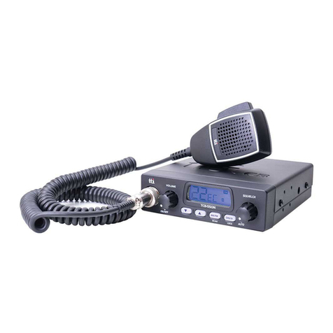
TTI TCB-1100 User manual

SERVICE MANUAL
TCB-1100
MULTI CHANNEL AM/FM TRANSCEIVER
TTI Tech Co.,Ltd.
Downloaded from www.cbradio.nl

TABLE OF CONTENTS
SECTION 1
SECTION 2
2-1
2-2
2-3
2-4
2-5
SECTION 3
SECTION 4
SECTION 5
5-1
5-2
5-3
5-4
5-5
5-6
SECTION 6
SECTION 7
SPECIFICATIONS
CIRCUIT DESCRIPTION
GENERAL
TECHNICAL DESCRIPTION
SEMICONDUCTORS AND FUNCTION
DESCRIPTION OF FREQUENCY DETERMINING AND STABILIZING CIRCUIT
TEST EQUIPMENT SETUP AND ALIGNMENT INSTRUCTIONS
PART LIST
MECHANICAL DISASSEMBLY
BOARD LAYOUT
MAIN PCB
LCD PCB
LED PCB
VOLUME PCB
SQUELCH PCB
CHANNEL PCB
BLOCK DIAGRAM
SCHEMATIC

General
Channel
Frequency Range
Operating mode
Frequency Control
Frequency Tolerance
Operating Temperature
Range
Microphone
Input Voltage
Size
Weight
Power Output
Modulation
Frequency Response
Output Impedance
Harmonic Suppression
Current Drain
40 (See the frequency band
chart)
26.96 MHz ~ 27.99125 MHz
F3E (FM), A3E (AM)
PLL Synthesizer
0.002%
-10 to + 55 C
Plug-in Type
13.2V DC 15%
190(W) x 165(L) x 58(H)
978.5 g
Duty cycle 10% 4 Watts @13.8V
DC
AM:from 85% to 95%
FM:1.8KHz to +2.0KHz
300Hz to 3000Hz
50ohms, Unbalanced
Less than -36dBm
Receiving System
IF Frequencies
Sensitivity
Audio Output Power
Audio Distortion
Image Rejection
Adjacent Channel Rejec-
tion
Conducted Spurious
Frequency Response
Built-in Speaker
Transmitter
Receiver
Dual conversion superheterodyne
Double Conversion 1st 10.695MHz/2nd 455KHz
0.7 V for 10dB(S+N)/N in AM Mode
0.7 V for 20dB SINAD in FM Mode
2.0W @ 8 Ohm
Less then 8% @ 1KHz
60 dB
60 dB
Less than -57dBm
300 to 2500Hz
8 Ohms, round
Adjustable; Threshold less than 1 microvolt
DSS; Less than 2 microvolt
Transmitter
General
SECTION 1. SPECIFICATIONS

SECTION 2. CIRCUIT DESCRIPTION
------------ Contents -------------
1 General
1-1. Receiver
1.2. Transmitter
2. Technical Description
2-1. General
2-2. Type of emission
2-3. Frequency Table
2-4. RF Power Output
2-5. DC input Voltage and Current with 13.2V DC Input to Power AMP
2-6. Receiver IF and Local Oscillator Frequencies
3. Semiconductors and Function
4. Description of Frequency Determining and Stabilizing Circuit
4-1. Introduction
4-2. Basic Synthesis Scheme
4-3. Descriptions of Each Block
4-3-1. Introduction
4-3-2. Reference Frequency
4-3-3. VCO
4-3-4. Programmable Divider and Its Control
4-3-5 Phase Detector and VCO Control
4-3-6. Transmitter / Receiver Buffer AMP
4-3-7. Transmitter Buffer Amp
4-3-8. Switching of Turning Capacitor in VCO
4-3-9. Receiver Local Oscillator Outputs
4-4. Frequency Stability
4-5. Description of other Circuits
4-5-1. Transmitter
4-5-2. Receiver
5. Test Equipment Setup and Test Procedure with Alignment Instructions
5-1. General Section.
5-1-2 Test Procedure with Alignment
5-2. T ransmitter Section
5-2-2. Test Procedure and Alignment at TX
5-3. Receiver Section
5-3-2 Test Procedure and Alignment at RX

TCB- 1100 Circuit Description Page 2
TTI 2009-02-20
1. General
1-1. Receiver
①Display : 40 Channels and other functions indication
②Frequency Range : 26.965 to 27.405 [MHz]
③Frequency Response : 300 to 2,500 [Hz]
④Power Source : 13.2 [V] DC
⑤Audio Output Load : 8 [OHM]
⑥Audio Output : 4.0 [W] (or More)
⑦Squelch : Adjustable from 0.2[uV] to 100 [uV]
⑧Sensitivity :
-FM : 20 dB [SINAD] under 1.0 [uV] RF Signal or less
-AM :10 dB [S/N] under 1.0 [uV] RF Signal or less
⑨Intermediate Frequency :
-1st IF : 10.695 [MHz]
-2nd IF : 455 [KHz]
1-2. Transmitter
①Carrier Power(Conducted) : AM 4[W] / FM 4 [W]
②Current Drain ( 13.2 [V] Supply Voltage)
-No Modulation : 1,100 [mA]
-Max Modulation : 1,600 [mA]
③Modulation Capabilities
-AM : ±90 [%]
-FM : ±1.8 [KHz/Dev]
④Spurious Radiation : Less then -54 [dBm]
⑤Antenna Impedance : 50 [OHM]
⑥Frequency Tolerance : 0.002 [%]

TCB-1100 Circuit Description Page 3
TTI 2009-02-20
2. Technical Description
2-1. General
Model TCB-1100 is an mobile type AM/FM radio transceiver for use of the Citizen Radio Service.
zFront Panel Controls
(1) LCD (Channel and RX/TX).
(2) Receiver Audio Control Volume (With Power ON/OFF Control)
(3) Squelch Control Volume (With DSS ON/OFF Control)
(4) Channel UP/Down Rotary Switch
(5) CH9 Select Key / Menu Key
(6) Scan Key / S.MEM Key
(7) DW Key / Vox Key
(8) Comp Key / Tone Key
(9) Back Light Select Key / Lock Key
(10) AM,FM Key / M Key
zAccessorily Connectors
(1) Antenna Socket
(2) External Speaker Jack (3.5mm)
(3) External S-meter Jack (2.5 mm)
(4) Microphone Connector (6 pin)
2-2. Type of emission : AM(A3E) , FM(F3E)

TCB-1100 Circuit Description Page 4
TTI 2009-02-20
2-3. Frequency Table
Channel Frequency (MHz) Channel Frequency (MHz)
1 26.965 21 27.215
2 26.975 22 27.225
3 26.985 23 27.235
4 27.005 24 27.245
5 27.015 25 27.255
6 27.025 26 27.265
7 27.035 27 27.275
8 27.055 28 27.285
9 27.065 29 27.295
10 27.075 30 27.305
11 27.085 31 27.315
12 27.105 32 27.325
13 27.115 33 27.335
14 27.125 34 27.345
15 27.135 35 27.355
16 27.155 36 27.365
17 27.165 37 27.375
18 27.175 38 27.385
19 27.185 39 27.395
20 27.205 40 27.405
2-4. RF Power Output
zAM : 4.0 [W]
zFM : 4.0 [W]
2-5. DC Iinput Voltage and Current with 13.2V DC Input to Power AMP
zTransmitter Power Amp : Voltage 12.0V
Current 900mA
zTransmitter Driver Amp : Voltage 12.0V
Current 130 mA
2-6. Receiver IF and Local Oscillator Frequencies
zFirst IF : 10.695 [MHz]
zSecond IF : 455 [KHz]
zFirst Local Oscillator : 10.695 [MHz] Upper Receiving Frequency
zSecond Local Oscillation : 10.240 [MHz]

TCB-1100 Circuit Description Page 5
TTI 2009-02-20
3. Semiconductors and Function
3-1. Transistor
--------------------------------------------------------------------------------------------------------------------------------------------
Ref No. Description Manufacturer Function
--------------------------------------------------------------------------------------------------------------------------------------------
Q101 2SC4226 NEC RX Amplifier
Q102 KTK211 KEC 1’st Mixer
Q103 KTK211 KEC 1’st Mixer
Q107 KTC3875SKEC RX,RF/Mute,at-TX
Q108KTC3875S KEC AGC
Q109 KTC3875S KEC AGC
Q110KRC112S KEC S-Meter Dectector
Q112 KRC112S KEC FM AF Mute at AM Mode
Q118 KRC111S KEC RX AF Mute at TX Mode
Q114 KTC3880S KEC AM IF Amplifier
Q115 KTC3880S KEC AM IF Amplifier
Q113 KRA101S KEC RX AM(B+)switch
Q116 KTA1504S KEC Automatic Noise Level Control
Q111 KTC3875S KEC RX FM AF Amp
Q121KTC1241 KEC TX,AM/1W-SW
Q132 KRC111SKEC TX,AM-AF,SW
Q201 KRC101S KEC AF Mute
Q117 KRC111S KEC AF Path
Q120KTA1504S KEC Automatic Level Control
Q119 KTC3875S KEC Automatic Level Control
Q128 2SC4226 NEC VCO
Q129 KTC3880S KEC RX/TX VCO Buffer
Q130 KTC3880S KEC VCO Buffer
Q127 KRC101S KEC TX VCO Control
Q133 KRC111S KEC TX,Call Switching
Q125KRC101S KEC TX Band2 Switching
Q155 KRC111S KEC TX,Mode Switching
Q146 KTC3875S KEC FM TX AF Mute at AM TX
Q134 KTC3880S KEC TX,Buffer
Q135 KTC3880S KEC TX Pre-Amplifier
Q1362SC2314F SANYO TX Driver Amplifier
Q138 RD16HHF1 Mitsubishi TX Power Amplifier
Q153 KTA101S KEC TX SW
Q8 KRC404 KEC CPU Reset
Q152 KRC101S KEC RX/TX Control
Q154 KRA101S KEC TX,SW
Q122 KRC101S KEC FM,AM,Switch
Q154KRA101S KEC TX,Switch
Q151 KRC111S KEC AM/FM,SW
Q145KRC102S KEC Power Low Control
Q143 KTC3875S KEC 8.2V Regulator
Q142 KTC3875S KEC RX B+
Q141KRA1504S KEC TX,B+
Q144 KTC3875S KEC 5V.Regulator
Q147 KRC111S KEC TX,Call-SW

TCB-1100 Circuit Description Page 6
TTI 2009-02-20
Q1 KTA1505S KEC Back-Light,LED-Control
Q2 KRC101SKEC Back-Light,LED-Control
Q3 KRC101S KEC Back Light LED Control
Q4 KRC101S KEC Back Light LED Control
Q5KRC110S KEC Back Light,LED Control
3-2. IC
--------------------------------------------------------------------------------------------------------------------------------------------
Ref No. Description Manufacturer Function
--------------------------------------------------------------------------------------------------------------------------------------------
IC1 SL5019 AUK IF IC
IC2 KIA358F KEC AGC, Squelch Control
IC3TDA2003 ST AF Power Amplifier
IC4LC7152NM SANYO PLL
IC5KIA4558F KEC FM TX AF
IC8 CMX138 CML Tone.IC
IC10 4094B Rohm Shift,Resistor
IC11 KIA2576 KEC Switchlng,Power-Supply
IC12 H8/38124 Renesas CPU
IC13 AT24C16 ATMEL EEPROM
IC14 KIA324 KEC Auto-SQ,Amp(DSS)
3-3. Manufacture Information
zKEC ---------------------- KEC Co., LTD.
zSANYO ---------------------- SANYO Semiconductor Co., LTD.
zTOKO ---------------------- TOKO, Inc.
zTOSHIBA ---------------------- Toshiba Semiconductor. Co., LTD.
zATMEL ---------------------- ATMEL Co., LTD
* NEC ----------------------- NEC Semiconductor
* AUK ----------------------- AUK Semiconductor
* Rohm ----------------------- Rohm Co.,Ltd
* Renesas ----------------------- Renesas Tech Nology Corp.

TCB-1100 Circuit Description Page 7
TTI 2009-02-20
4. Description of Frequency Determining and Stabilizing Circuit
4-1. Introduction
The Frequencies for transmitter and receiver first local frequencies are all derived from a signal
4.5MHz crystal by means of a phase locked loop(PLL).
The first local oscillator frequencies are 37.660MHz(CH1) to 38.10MHz(CH40). The second local
frequency is fixed at 10.240MHz to generate second IF 455KHz.
Transmit, the VCO of the PLL operates 26.965MHz(CH1) to 27.405MHz(40CH). The VCO frequency
goes to the Buffer Amp circuit Q134, L701.
Q128
VCO Q134
Buffer
26.965MHz(CH1)
~
27.405MHz(CH40)
26.965MHz(CH1)
~
27.405MHz(CH40)
To transmitter
The VCO operating frequency for the receiver is 37.66MHz(CH1) to 38.10MHz(CH40) as the
first local oscillator, injected through the buffer amplifier Q129into the first FET balanced mixer Q102,
Q103.
4-2. Basic Synthesis Scheme
The crystal frequency(4.5MHz) is divided by 1800 times to make 2.5KHz which is fed to one
side of the phase detector. The VCO output is divided by a programmable divider, and fed to other side of
the phase detector Pin 9, 10 of IC4. Passing the phase detector output closes the feedback loop through
an active low pass filter and using the output to control the VCO frequency through varicap diode D112.
Under locked conditions, both of phase detector input signal must be identical at 2.5KHz.
The VCO frequency is then given by ;
Receiver : Fvco / N = 0.005 [MHz] OR Fvco = 0.005 X N [MHz]
Transmitter : Fvco / N = 0.005 [MHz] OR Fvco = 0.005 X N [MHz]
Since “N” is an integer, the VCO frequency can be stepped up with in receiver mode 5KHz and
transmitter mode 5KHz increments.
By suitable choice of “N” the desired output frequency can be obtained.
Channel 1 Channel 40
N Fvco N Fvco
Transmit 5393 26.965 5481 27.405
Receiver 7532 37.660 7620 38.100
The VCO frequency goes to the Buffer Amp circuit,
VCO Output Frequency Buffer Output Frequency

TCB-1100 Circuit Description Page 8
TTI 2009-02-20
Transmit
---
---
---
Transmit
CH 1 , 26.965 MHz
CH 40 , 27.405 MHz
26.965 MHz
27.405 MHz
Since all frequencies are obtained from the crystal controlled PLL oscillator, all outputs are
coherent with the crystal oscillator frequency and matching the sample percentage accuracy.
Note that the reference frequency of 5KHz, receiver and transmitter is obtained by
dividing the 4.5MHz by 900 times and 1800 times

TCB-1100 Circuit Description Page 9
TTI 2009-02-20
4-3. Descriptions of Each Block
4-3-1. Introduction
The synthesizer is implemented with the following components;
PLL IC (IC4)
X-TAL (X102)
VCO, VARICAP DIODE (D112)
IC4is CMOS LSI that includes most of PLL block.
The Q128, L301, C232, C242, C243, C244, varicap diode D112are clap oscillator circuit to
operate as a VCO of the IC4. Q127 is a switching transistor to connect or disconnect the tuning
capacitor in the VCO oscillator tank circuit for transmitter or receiver.
Q129 works as a buffer amplifier for RX local frequencies (≒37MHz) and TX carrier
generating frequencies(≒26MHz)
4-3-2. Reference Frequency
The crystal X102(4.5MHz) and other components at Pin 1 and 24 of IC4can make a reference
frequency oscillator with internal amplifier.
4-3-3. VCO
Q128 and surrounding parts are consisting a clap oscillator works as a VCO of IC4. With
appropriate control voltage on D112 the VCO can be oscillate over the required range of 26.965MHz to
38.10MHz.
4-3-4. Programmable Divider and Its Control
The programmable input for each channel are stetted by the PLL Clock(Pin 56), PLL Data(Pin
55), PLL Enable(Pin 58) of IC12. Each input signal to control the PLL ic is done with provide key input
Pin 73, 74, 75. For each key input, an internal code converts EEPROM
appropriate control to the programmable divider for that channel.
Since the change transmit and receive, and additional bit is required at Pin 66 of IC12 to allow
the ROM to recognize the status TX or RX.
During transmit the push to talk switch makes Pin 66 ground, PLL IC works
under transmit status.
The programmable divider output fed to the phase detector for compare with the 5KHz
reference frequency IC4. See table 1 for actual input and divide ratio on all channels.
4-3-5. Phase Detector and VCO Control
The phase detector is a digital phase comparator witch compares the phase of the reference
signal with programmable divider output square waves and develops a series of pulses whose dc level
depends on the phase error of each signal.
The phase detector pulse output is fed to an active low pass filter and RC low pass filter output
signal of IC4is filtered and fed to varicap D112control the VCO frequency.
4-3-6. Transmitter / Receiver Buffer AMP
Output signal of Q128 is fed into the buffer amplifier Q129, L3 to generate TX carrier
frequency and 1’st local frequencies.

TCB-1100 Circuit Description Page 10
TTI 2009-02-20
4-3-7. Transmitter Buffer
The output signal of Q129, L3 goes to an amplifier with tuning circuit Q134, L701,
which bufferincoming 26MHz signals.
4-3-8. Switching of Turning Capacitor in VCO
The VCO circuit must tune with a wide range of frequencies 26.965MHz ~ 27.405MHz for
transmitter and 37.66MHz ~38.10MHz for receiver.
To comply above range of VCO, the tuning capacitance should switch for transmission. The
tuning circuit consists with L301, C232, C242, C243, and C244. When the VCO is working as a receiver
Q127 becomes turn OFF. So, L301 and C232, D112makes turning function.
When transmitting, Q127 becomes ON. S the o, L301 an parallel capacitance of C232 and C241
make turning function.
4-3-9. Receiver Local Oscillator Outputs
zFIRST MIXER :
The secondary output signal of L107 is injected to the sources of 1’st mixer Q102, Q103 in the
1’st IF mixer section.
zSECOND MIXER :
The output of 10.24MHz oscillator circuit with X101 is injected into the IF IC(IC1) internally.
Incoming IF signal and 10.24MHz signal are mixed inside the IF IC to extract 2’nd IF signal 455KHz.
FM audio Signals are recovered with the way of quadrature detector.
AM signals are recovered with envelope detector.
4-4. Frequency Stability
Let : Fo = Crystal oscillator frequency
Fr = Phase detector reference frequency
Fvco = VCO frequency
Ft = Transmit frequency
Then : Receiver : Fr = Fo/900
Transmitter : Fr = Fo/900
And under locked conditions : Fr = Fvco / N
Where, “N” is the programmable divider divide ratio.
Then : Fvco = N X Fr)
From which it can be seen, the percentage error in Ft is the same as the percentage error in Fo.
The stability of the crystal oscillator is determined primarily by the crystal itself and having lesser
deviation by the active and passive components of the oscillator. The choice of crystal and components is
such that the required frequency stability is maintained over the required voltage and temperature range.

TCB-1100 Circuit Description Page 11
TTI 2009-02-20
4-5. Description of other Circuits
4-5-1. Transmitter
A. RF Amplification
RF carrier frequencies are obtained at the output of buffer amplifier Q134 and turning IFT coil
L701, The input of VCO frequencies 26MHz is selected at the buffer output,
The output of buffer amplifier Q134 is fed through turning IFT coil L701, L703to the base of pre driver
amplifier Q135. It’s output; 27MHz is coupled to RF driver amplifier Q136, a low-level class C power
amplifier. Driver Q136 supplies the necessary power gain to operate RF final Q138 at
the maximum efficient. The output of Q138 is supplied to the antenna through L-C turning circuit.
B. Circuit for Suppression of Spurious Radiation
The turning circuit between the output of final amplifier Q138 and antenna, 4-stage “π”
network C322, C323, C324, L711, C325, C326, L712, C328, C329, L713, C331, C332, C333, L714,
C334serves as a spurious radiation suppressor. This network also servers to match the impedance
between TX power amplifier Q138 and the antenna.
C. Circuits for Limiting Power
After finished all alignment, the constant voltage supply circuit limits the available power 4W or
slightly less. RV106 and corresponding three-transistor control supply voltage of RF power amplifier.
When power low switch function Q145changed the supply voltage. Tune all the trimming parts for
maximum indication of RF power meter and adjust RV104 to make 4W indication of RF power meter.
After finishing the above adjustments check the RF power meter reading is changed 1W under “LOW”
state.
The turning is adjustment so that the actual power is from 3.8W to 4.0W. There are no other
additional controls for adjusting the TX output power.
D. Modulation Control
Modulation of the RF is a process that begins with the audio picked up by the microphone.
<FM>
The microphone input is fed to mic audio amplifier IC5that drives modulation vricap diode
D113 in the VCO circuit RV107 limits the incoming modulation audio levels to inhibit over modulation.
While reading the modulation factor on the modulation analyzing equipment, adjustment RV107 shall not
exceed 2.0KHz deviation.
<AM>
Modulation signals are filtered with RC network and goes to the audio power amplifier IC3in
to make normal signal level to achieve wanted modulation. IC3drives T101, which is a combination
AF output/modulation transformer. During transmit, one of the secondary windings of T101 is tied
between the 13.2V DC supply and the collectors of RF driver Q136and RF power amplifier Q138. As the
audio passes through T101 it causes the collector supplies of Q136 and Q138 to vary with audio,
producing an AM signal at carrier frequency.
To avoid over modulation of the carrier, a protection of the modulating signal is fed back from
the T101 through the AMC circuit, Q119 and Q120, to control the gain of IC3and sets the maximum
level of modulation. Form the center tab of RV102 and Q120 the feedback signal is rectified by diode
D109, filtered by C202, and supplied the Q119. The collector of Q119 is tied directly TX audio input to
control gain. That is, when the audio output is higher that the preset level of RV102, the information is
reflected through Q119 and Q120, reducing the gain of IC3

TCB-1100 Circuit Description Page 12
TTI 2009-02-20
4-5-2. Receiver
Overload protection is provided to receiver’s semiconductors by diode D101. These diodes have
a little effect on the incoming signal from another CB station; they protect the receiver from stray
transmitter energy.
In the receiver mode of operation, Q142 transistor is turned on. Also bias voltage is applied to
Q101, Q102, Q103, IC1.
Q101 is a 27MHz RF input amplifier, and any excessive input signal is limited by diode D101.
CB receiver is dual conversion super-heterodyne type with the first IF 10.695MHz and the
second IF 455KHz.
Receiver is separated to blocks, 1’st IF section and 2’nd IF section. The PLL synthesizer
supplies 1’st local frequency 37.660MHz ~ 38.10MHz. The amplified 27MHz is mixed. With the
provide 1’st local frequencies Q102, Q103 mixes the incoming RF signal to generate 1’st IF signal. The
resulting first IF is 10.695MHz. Q102 and Q103 is the first converter, and 10.695MHz is sharply filtered
by L108 and crystal filter XF101. The first IF is again mixed with a second local oscillator of 10.24MHz.
With the 10.240MHz signal, IC1 FM IF IC converts the incoming signals to generate 2’nd IF
signal and recovered audio signals. 2’nd IF is filtered by a razor sharp ceramic filter CF101 coupled. The
455KHz signal from the 2’nd IF filter was amplified and limits internally. After amplification the signals
fed to the quardrature detector loop L109. Then could see the recovered signals Pin 8of IC1.
With the amplitude of recovered signals, Q111 serves as an amplifier.
AM signals from the Pin 5of IC1 were tapped with C135 and amplified two-stage amplifier
Q114, Q115. Q114is a first 455KHz amplifier, and the Q114being the last amplifier. D107 is a detector
diode witch produce audio signal as well as negative DC voltage for AGC action. The negative voltage
also provides forward biasing to the emitter of ANL clipping transistor Q116. The biasing voltage has a
time constant determined R162 and C168. Therefore any sharp negative going pulse from D107 will back
bias Q116 and clipped. The way to recover the AM information audio is envelope detector.

TCB-1100 Circuit Description Page 13
TTI 2009-02-20
5. Test Equipment Setup and Test Procedure with Alignment Instructions
5-1 General Section
5-1-1 Test Equipment Required
•DC power supply(13.8V/3A)
•DC Voltmeter or Oscilloscope
•RF attenuator (30dB)
5-1-2 Test Procedure and Alignment
Step Setting Connection Adjuster Adjust for
1 RX VCO voltage Adj.
Channel & Frequency :
1CH, 26.956 MHz
Mic : Receive
Volume : Optional
Squelch : Optional
DC voltmeter to VCO
Test point (Figure 1) L301 1.9~2.1V DC
2 TX VCO voltage Adj.
Channel & Frequency :
1CH, 26.956 MHz
Mic : Transmit(No Mod)
Volume : Optional
Squelch : Optional
DC voltmeter to VCO
Test point (Figure 1) L301 4.8~5.0 V DC
Figure 1

TCB-1100 Circuit Description Page 14
TTI 2009-02-20
5-2 Transmitter Section
5-2-1 Test Equipment Required
•RF Power Meter •DC power supply(13.8V/3A)
•50 ohms load (non-inductive) •Spectrum analyzer
•RF attenuator (30dB) •Frequency counter
•Oscilloscope •Coupler
•Audio generator •Modulation meter
5-2-2 Test Procedure and Alignment
Step Setting Connection Adjuster Adjust for
1 RF Power Adj.
Channel : 19CH
Function : AM or FM Mode
MIC : Transmit
Volume : Optional
Squelch : Optional
Connect dummy load and RF
Power Meter to the EXT–ANT
connector on the set(Figure 3)
L701
L703
Maximum
indication on
the Power
Meter(4.0W).
If indication is
not in 4W
range, ACP
Adjustment(R
V104)
2 Frequency Adj.
Channel & Frequency :
19CH, 27.185 MHz
Function : AM or FM Mode
Mic : Transmit(No Mod)
Volume : Optional
Squelch : Optional
Connect dummy load and
Frequency Counter through
Coupler to RF Power Meter.
Connect RF Power Meter to
EXT-ANT connector on the
set(Figure 2).
CT1Be sure that
the indication
of the
transmitter
frequency is
27.185MHz
±300 Hz on
the Frequency
Counter
3 AM Modulation Adj.
Channel & Frequency :
19CH, 27.185MHz
MIC: Transmit
Function : AM Mode
Volume : Optional
Squelch : Optional
Connection the audio
generator (set to 1 KHz)to the
microphone.
Connect the modulation meter
through the RF attenuator to
the ANT Connector. Adjust
the audio signal level to obtain
by 50% modulation.
When you increase the audio
signal by 20 dB, the
modulation should not exceed
90% Modulation(Figure 3).
RV102 80% ~ 90%

TCB-1100 Circuit Description Page 15
TTI 2009-02-20
4 FM Deviation Adj.
Channel & Frequency :
19CH, 27.185MHz
MIC : Transmit
Function : FM Mode
Volume : Optional
Squelch : Optional
Connection the audio
generator (set to 1 KHz)to the
microphone.
Connect the modulation meter
through the RF attenuator to
the ANT Connector. Adjust
the audio signal level to obtain
by 1KHz deviation.
When you increase the audio
signal by 20 dB, the deviation
should not exceed 2.0KHz
deviation(Figure 3).
RV1071.8KHz ~
2.0KHz
Figure 2
Figure 3

TCB-1100 Circuit Description Page 16
TTI 2009-02-20
5-3 Receiver Section
5-3-1 Test Equipment Required
•Standard Signal Generator(SSG)
•DC power supply(13.8V/3A)
•AC Level Meter
•Distortion Meter
•Oscilloscope
•SINAD Meter
•8 ohm Dummy Load
5-3-2 Test Procedure with Alignment
Step Setting Connection Adjuster Adjust for
1 AM Audio Output Adj.
Channel & Frequency :
19CH, 27.185MHz
MIC : Receive
Function : AM Mode
Volume : Full clockwise
Squelch : Turn to counter
clockwise
Connect RF Signal Generator
to EXT-ANT Connector.
Connect AC Level Meter and
Distortion Meter and SINAD
Meter across EXT SPK jack
with 8 ohm Dummy
Load(Figure 4)
L101
L103
L104
L105
L107
L108
L110
Maximum
indication on
AC Level
Meter. Reduce
output from
SSG until the
audio output
becomes about
2V.
2 FM Audio Output Adj.
Channel & Frequency :
19CH, 27.185MHz
MIC : Receive
Function : FM Mode
Volume : Full clockwise
Squelch : Turn to counter
clockwise
Connect RF Signal Generator
to EXT-ANT Connector.
Connect AC Level Meter and
Distortion Meter and SINAD
Meter across EXT SPK jack
with 8 ohm Dummy
Load(Figure 4)
L109 Maximum
indication on
AC Level
Meter. Reduce
output from
SSG until the
audio output
becomes about
2V.
3 Squelch Adj.
Channel & Frequency :
19CH, 27.185MHz
MIC : Receive
Function : FM Mode
SSG : 27.185MHz, 1KHz,
100uV, 1.2KHz Dev.
Volume : Full clockwise
Squelch : Full clockwise
clockwise
Connect RF Signal Generator
to EXT-ANT Connector.
Connect AC Level Meter and
Distortion Meter and SINAD
Meter across EXT SPK jack
with 8 ohm Dummy
Load(Figure 5)
RV101 Adjust until
the audio
output
appears.

TCB-1100 Circuit Description Page 17
TTI 2009-02-20
Figure 4
Other manuals for TCB-1100
1
Table of contents
Other TTI Transceiver manuals

TTI
TTI TCB-660 User manual

TTI
TTI TCB-R2000 User manual

TTI
TTI TCB-550 User manual
TTI
TTI Freequency TCB-770 User manual
TTI
TTI Freequency TCB-770 User manual
TTI
TTI Freequency TCB-880 User manual
TTI
TTI TCB-660 User manual
TTI
TTI Freequency TCB-880 User manual
TTI
TTI TCB-H100 User manual

TTI
TTI TCB-560 User manual
