Wavelength Electronics LDTC2/2 User manual

LDTC2/2 Laser DIode Driver and Temperature Controller
www.teamwavelength.com© 2005 PRELIMINARY LDTC2/2-00400-A Rev A
TOP VIEW
GENERAL DESCRIPTION:
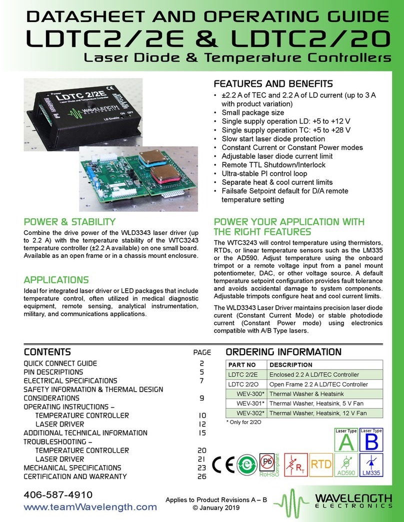
The LDTC 2/2 combines a 2.2 Amp laser driver
and 2.2 Amp temperature controller on one
small board. Available as an open frame or in a
chassis mount enclosure.
The WTC3243 will control temperature using
thermistors, 100ΩPlatinum RTDs, or linear
temperature sensors such as the LM335 or
the AD590. Adjust temperature using the
onboard trim pot or a remote voltage input from
a panel mount potentiometer, DAC, or other
voltage source. A default temperature set point
configuration provides fault tolerance and avoids
accidental damage to system components.
Adjustable trim pots configure heat and cool
current limits.
The heart of the laser driver section is the
WLD3343 2.0 Amp Laser Driver. It maintains
precision laser diode current (Constant Current
mode) or stable photodiode current (Constant
Power mode) using electronics compatible with
A/B Type lasers.
Ideal for higher power laser diodes for medical
diagnostic equipment, remote sensing, and
analytical instrumentation.
Combine the drive power of the WLD3343 with
the temperature stability of the WTC3243
FEATURES:
• Small package size
• Single supply operation
• Cost Effective
FEATURES, Laser Diode Driver:
• Default current range is 2.2A. Custom ranges,
from 3mA up, easily configured.
• Slow start laser diode protection
• Constant Current or Constant Power modes
• Compatible with A or B type laser diodes
• Adjustable laser diode current limit
• Remote TTL Shutdown / Interlock
FEATURES, Temperature Controller:
• Drive up to 2.2A of TEC current
• Set temp using D/A - includes default to near
room temperature to avoid drive when D/A is
turned off or signal lost
• Ultra-stable PI control loop
• Separate Heat & Cool current limits
• Single power supply operation
August, 2005
Figure 1
Top View Pin Layout
and Descriptions
LDTC2/2
1
11
CC
CP
+
S2
ON
OFF
Tset LIMA LIMB ILIM ISET
+
+
D1
D2
J1 J2
J3
J4
ExtTset Vset PDset
R2
R3
R4
R5
R6
COM
SEN-
SEN+
TEC-
TEC+
COM
LDA
PDC
PDA
LDC
GND
VS
VDD
COM
R TC SET
SET T M
ACT T MON
LD I MON
LD P MON
COM
R LDSET
COM
LD SHD
SP2
SP1
3
2
1
10
9
8
7
6
5
4
3
2
1
12
11
10
9
8
7
6
5
4
3
2
1
R SENSE
LD
ENABLE
POWER
ON
LD ENABLE
TOGGLE
SWITCH
Fan Power

www.teamwavelength.com© 2005 PRELIMINARY
LDTC2/2
PAGE 2
LDTC2/2-00400-A Rev A
TYPE A TYPE B
Works with these LASER DIODE TYPES
BLOCK DIAGRAM
Schematic for WLD3343 connections
SHD
1
VSET
2
IMON
3
PMON
4
MODE
5
LIM
6
GND
7RS+ 8
B9
RS- 10
A11
PD+ 12
PD- 13
VDD 14
U2
WLD3343
R15
0.20 2512 1.0W
R14
0.20 2512 1.0W
+1
-- 2
3
VR2
LM4040AIM3-2.5
2
3
1
411
U4A
13
12
14
411
U4D
IMON
2
1
3S1
GT11MCKE
PMON
VDD
D1
LED
Remote Enable
CW 3
W
2
CCW
1
R5
500
1
2
3
JP3
HEADER 3
Shown in CC
LDC
PDA
PDC
LDA
VDD
VDD
VDD
VDD
Ext Vset
LIM
S2
EG2211
R23
1.00K
R22
1.00K
R17
1.00K 1%
R7
1.00K
R19
1.00K
R21
4.99K
R18
150
R16
10K
2
3
1
411
U6A
5
6
7
411
U6B
9
10
8
411
U6C
13
12
14
411
U6D
R11
1.00K
R10
1.00K
R12
1.00K
R9
1.00K
R8
10K
1
2
3
JP2
HEADER 3
VDD
VDD
VDD
R13
1.00K
MOD
1
2
J4
Fan Power
VDD
R37
1.00K 1%
VDD
1
2
3
4
5
6
7
8
9
10
J3
CON10
VDD
Common
Common
TEC+
TEC-
Sensor+
TEC+
TEC-
Sensor+
Sensor-
CW 3
W2
CCW
1
R6
5K
+
C15
4.7UF 16V
C17
0.1UF 50V
C18
0.1UF 50V
C16
0.1UF 50V
+
C14
4.7UF 16V
C7
0.1UF 50V
R20
499
OFF
ON

www.teamwavelength.com© 2005 PRELIMINARY
LDTC2/2
PAGE 3
LDTC2/2-00400-A Rev A
BLOCK DIAGRAM
Schematic for WTC3243 connections
VDD
1
VSET
2
LIMA
3
LIMB
4
P
5
+1V
6
I
7SG 8
S+ 9
BIAS 10
OUTA 11
OUTB 12
GND 13
VS 14
U1
WTC3243
+1
-- 2
3
VR1
LM4040AIM3-2.5
VDD
5
6
7
411
U4B
9
10
8
411
U4C Set T
ACT T
CW 3
W
2
CCW
1
R3
5K
CW 3
W2
CCW
1
R4
5K
VDD
VDD
VDD
LIMA LIMB
VDD
VS
VDD VS
100uA
VDD
VS
VCC
D2 power
R24
1.00K
R25
1.00K 1%
R34
1.00K
R29
1.5K
R28
1.5K
VIN
2
GND
3
3.3V 1
U8
LM3480IM3-3.3
VCC
Vset/DAC
VDD
VDD
VDD
VCC
VCC
VCC
R35
20.0K
1
2
3
4
5
6
7
8
9
10
11
12
J2
CON12
ACT T
SET T
GNDACT T
SET T
Common
Common
TEC+
TEC-
Sensor+
R33
10.0K
R32
100K
1
2
3
J1
CON3
VDD
PMON
IMON
Ext Vset
Remote Enable
PMON
IMON
Ext Vset
Rem En
Common
Spare1
Spare2
NO 6
COM 5
NC 4
IN
1
V+
2
GND
3
U7
ISL84544
R1
1.00K 1%
74
3
2
6
+
_U3
OP777AR
2
3
1
84
U5A
OP727ARU OS
5
6
7
84
U5B
OP727ARU OS
1
2
3
JP1
HEADER 3
R36
348K 1%
R26
10.0K
R27
4.99K
CW 3
W2
CCW
1
R2
5K
+
C5
68UF 16V
+
C2
4.7UF 50V
+
C1
4.7UF 16V
+
C8
4.7UF 50V
+
C9
4.7UF 50V
C11
0.1UF 50V
C10
0.1UF 50V
C6
0.1UF 50V
C12
0.1UF 50V C13
0.1UF 50V
C3
0.1UF
C4
0.1UF
R30
24.9K
R31
31.6K
R38
150

www.teamwavelength.com© 2005 PRELIMINARY
LDTC2/2
PAGE 4
LDTC2/2-00400-A Rev A
Supply Voltage (Voltage on Pin 14)
Output Current (See SOA Chart)
Power Dissipation, TAMBIENT = +25˚C
ELECTRICAL AND OPERATING SPECIFICATIONS
Volts DC
Amperes
Watts
UNITVALUE
+4.5 to +12
2.2
9
VDD
ILD
PMAX
ABSOLUTE MAXIMUM RATINGS
WLD3343 Laser Diode Driver Rating SYMBOL
Note [1]. With Revision D of the WLD3343, an internal thermostat has been added to activate Shutdown (SHD) when
the internal temperature exceeds 105˚C. The output will be re-enabled after a 250 to 300 msec slow-start once the
internal temperature drops below 95˚C.
ppm
%
Amps
Volts
nsec
nsec
MHz
Seconds
Volts
mA
mV
nA
V
dB
dB
˚C/W
˚C/W
˚C/W
Sec
75
0.05
2.2
12
15
5
50
VDD
33
25
3.9
50
2.0
160
320
1.6
0.25
10
1
20
85
80
30
21.5
3.4
10
0.02
1.8
3.0
5
5
0
60
60
28
18
3.1
CONSTANT CURRENT CONTROL
Long Term Stability, 24 hours
CONSTANT POWER CONTROL
Long Term Stability, 24 hours
OUTPUT
Current, peak, see SOA chart
Compliance Voltage, Laser Diode Load
Rise Time
Fall Time
Bandwidth
Bandwidth
Slow Start
POWER SUPPLY
Voltage, VDD
Current, VDD supply, quiescent
INPUT
Offset Voltage, initial, Imon
Bias Current (based on input Res of op amp)
Common Mode Range
Common Mode Rejection, Set point
Power Supply Rejection
THERMAL
Heatspreader Temperature Rise
Pin Solderability
TYPMIN MAX UNITSTEST CONDITIONSLaser Diode Driver PARAMETER
TAMBIENT = 25˚C
TAMBIENT = 25˚C
With Heat Sink and Fan
Full Temp. Range, ILD = 2.0 Amps, 5V
ILD= 2 Amps
ILD= 2 Amps
Constant Current, Sine Wave
Constant Power (Depends on PD BW)
Pin 2, TAMBIENT = 25˚C, VCM = 0V
Pin 2, Full Temp. Range
Full Temperature Range
TAMBIENT = 25˚C
With WHS302 Heat sink, WTW002
Thermal Washer
With WHS302 Heat sink, WTW002
Thermal Washer and 3.5 CFM fan
Solder temp @260˚C
Supply Voltage 1 (Voltage on Pin 1)
Supply Voltage 2 (Voltage on Pin 14)
Output Current (See SOA Chart)
Power Dissipation, TAMBIENT = +25˚C (See SOA Chart)
(with fan and heat sink)
VDD
VS
IOUT
PMAX
+4.5 to +12
+4.5 to +30
±2.5
9
Volts DC
Volts DC
Amperes
Watts
SYMBOL VALUE UNIT
WTC3243 Temperature Controller Rating
Operating Temperature, case [1]
Storage Temperature
Weight - with enclosure
Weight - open frame
˚C
˚C
oz
oz
- 40 to + 85
- 65 to +150
TOPR
TSTG
LDTC2/2E
LDTC2/2O
SYMBOL VALUE UNIT

www.teamwavelength.com© 2005 PRELIMINARY
LDTC2/2
PAGE 5
LDTC2/2-00400-A Rev A
Short Term Stability, 1 hour
Long Term Stability, 24 hour
Control Loop
P (Proportional Gain)
I (Integrator Time Constant)
Setpoint vs. Actual T Accuracy
OUTPUT
Current, peak, see SOA Chart
Compliance Voltage,
Pin 11 to Pin 12
Compliance Voltage,
Pin 11 to Pin 12
Compliance Voltage,
Pin 11 to Pin 12
Compliance Voltage,
Pin 11 to Pin 12
Compliance Voltage,
Resistive Heater
POWER SUPPLY
Voltage, VDD
Current, VDD supply, quiescent
Voltage, Vs
Current, Vs supply, quiescent
INPUT
Offset Voltage, initial
Bias Current
Offset Current
Common Mode Range
Common Mode Rejection
Power Supply Rejection
Input Impedence
Input voltage range
TSET = 25˚C using 10 kΩthermistor
Full Temp. Range, IOUT = 100 mA
Full Temp. Range, IOUT = 1 Amp
Full Temp. Range, IOUT = 1.5 Amps
Full Temp. Range, IOUT = 2.0 Amps
Pins 2 and 9
Pins 2 and 9, TAMBIENT = 25˚C
Pins 2 and 9, Full Temp. Range
Full Temperature Range
0.001
0.003
P
18
2
±2.0
| VS- 0.7 |
| VS- 1.2 |
| VS- 1.6 |
| VS- 1.8 |
| VS- 1.7|
4.5
4.5
20
0
60
60
GND
0.005
0.008
PI
20
3
<0.2%
(Rev B)
±2.2
| VS- 0.5 |
| VS- 1.0 |
| VS- 1.4 |
| VS- 1.6 |
| VS- 1.6 |
55
50
1
20
2
85
80
500
0.010
0.010
22
4
± 2.5
12
105
28
100
2
50
10
VDD-22
VDD-22
˚C
˚C
A/V
Sec.
Amps
Volts
Volts
Volts
Volts
Volts
mA
Volts
mA
mV
nA
nA
V
dB
dB
kΩ
Volts
Temperature Control
PARAMETER
TEMPERATURE CONTROL
TEST CONDITIONS MIN TYP UNITSMAX
2The bias source has a compliance up to VDD - 2.0 V. In normal operation this limits the sensor voltage range tp
0.25V to VDD - 2.0V. While voltages up to +/- 5V outside this range on the Vset pin will not damage the unit, it will
not provide proper control under these conditions.
NOTE: Operation higher than 5V on VDD (i.e. 12V) requires close evaluation of the SOA curves and
current limit settings. Damage to the WLD or WTC will occur if they are operated outside their Safe
Operating Area. Contact the factory if you plan to use higher than 5V.
ELECTRICAL AND OPERATING SPECIFICATIONS, continued

www.teamwavelength.com© 2005 PRELIMINARY
LDTC2/2
PAGE 6
LDTC2/2-00400-A Rev A
Connect +5 to +12V between pins 2 & 3 to power the control
electronics and the output drive to the Laser Diode. Use the
ONLINE Safe Operating Area calculator to make sure maximum
internal power dissipation in the WLD is not exceeded - especially
when using greater than +5V.
Connect +5 to +28V between pins 1 & 3 to drive the TEC
output stage - Use the ONLINE Safe Operating Area calculator to
make sure maximum internal power dissipation in the WTC is not
exceeded - especially when using greater than +5V.
Spare connection for your use - test point, etc.
Float or GND = Enable Laser Diode Current
Input >3V = Disable Laser Diode Current
Low current GND for monitors, DACs, External VSET, etc.
Voltage Input range is 0 to 2V. Transfer function:
VR LDSET = ILD * (2 RSENSE)
Low current GND for monitors, DACs, External VSET, etc.
Monitor the laser diode power. The Photodiode Current Monitor
produces a voltage proportional to the current produced by the
laser diode monitor photodiode.
Monitor the laser diode forward current. The Laser Diode Current
Monitor produces a voltage proportional to the current flowing
through the laser diode.
Monitor the actual voltage produced by the temperature sensor.
The voltage produced and transfer function to temperature is
determined by the sensor chosen.
Monitor the temperature setpoint voltage. The voltage produced
and transfer function to temperature is determined by the sensor
chosen.
Connect a voltage source between Pin 11 (VSET) and Pin 12
(GND) to control the temperature setting remotely. A default
value of 1V (about room temperature with 10kΩthermistor) will be
seen by the WTC if the voltage at this pin drops below 0.3V.
Low current GND for monitors, DACs, External VSET, etc.
Cooling current flows from this pin when using an NTC sensor.
Heating current flows from this pin when using an NTC sensor.
Connect resistive and LM335 type temperature sensors across
Pin 8 and Pin 9. Connect a 10 kΩ resistor across these pins when
using AD590 type temperature sensors. The negative terminal of
the AD590 sensor connects to Pin 8 and the positive terminal to
Pin 1 (VDD) of Connector 1. AD590 operation requires that VDD
be +8 Volts or greater for proper operation.
Low current GND for monitors, DACs, External VSET, etc.
PIN DESCRIPTIONS
Supply Voltage to Control
Electronics and Laser
Diode
Supply Voltage to Output
TEC Drive
Power Supply Ground
Spare 1
Spare 2
LD Shutdown / Interlock
Common
Remote Laser Diode
Setpoint
Common
Photodiode monitor
LD Current monitor
Actual Temp monitor
Setpoint monitor
Remote Temperature
Setpoint
Common
Laser Diode Cathode
Photodiode Anode
Photodiode Cathode
Laser Diode Anode
Common
TEC + connection
TEC - connection
Temperature Sensor +
Temperature Sensor -
Common
VDD
VS
GND
SP1
SP2
LD SHD
COM
R LDSET
COM
LD P M
LD I M
ACT T M
SET T M
R TCSET
COM
LDC
PDA
PDC
LDA
COM
TEC+
TEC-
SEN+
SEN-
COM
1
2
3
1
2
3
4
5
6
7
8
9
10
11
12
1
2
3
4
5
6
7
8
9
10
Connector 1 (J1)
Pin Pin # Name Function
Connector 2 (J2)
Connector 3 (J3)

www.teamwavelength.com© 2005 PRELIMINARY
LDTC2/2
PAGE 7
LDTC2/2-00400-A Rev A
TYPICAL PERFORMANCE GRAPHS - WLD
Caution:
Do not exceed the Maximum Internal Power Dissipation of the WLD or WTC.
Safe Operating Area (SOA) tools are provided online to make your design easier.
Exceeding the Maximum Internal Power Dissipation voids the warranty.
To determine if the operating parameters fall within the SOA of the device, the maximum voltage drop across the driver
and the maximum current must be plotted on the SOA curves.
These values are used for the example SOA determination for a WLD:
Vs = 12 volts
VLoad = 5 volts
ILoad = 1 amp
Follow these steps:
1. Determine the maximum voltage drop across the driver,Vs-VLoad, and mark on the X axis.
Example: 12 volts - 5 volts = 7 volts, Point A)
2. Determine the maximum current, ILoad, through the driver and mark on the Y axis:
(1 amp, Point B)
3. Draw a horizontal line through Point B across the chart. (Line BB)
4. Draw a vertical line from Point A to the maximum current line indicated by Line BB.
5. Mark VSon the X axis. (Point C)
6. Draw the Load Line from where the vertical line from point A intersects Line BB down to Point C.
Refer to the chart shown below and note that the Load Line is in the Unsafe Operating Areas for use with no heatsink
(1) or the heatsink alone (2), but is outside of the Unsafe Operating Area for use with heatsink and Fan (3).
An online tool for calculating your load line is at http://www.teamwavelength.com/tools/calculator/soa/defaultld.htm
These values are determined from the specifications of the laser diode.
}
Graphs assume:
25°C Case
A
BBB
C

www.teamwavelength.com© 2005 PRELIMINARY
LDTC2/2
PAGE 8
LDTC2/2-00400-A Rev A
TYPICAL PERFORMANCE GRAPHS - WTC
Caution:
Do not exceed the Maximum Internal Power Dissipation of the WLD or WTC.
Safe Operating Area (SOA) tools are provided online to make your design easier.
Exceeding the Maximum Internal Power Dissipation voids the warranty.
To determine if the operating parameters fall within the SOA of the device, the maximum voltage drop across the
controller and the maximum current must be plotted on the SOA curves.
These values are used for the example SOA determination for a WTC:
Vs= 12 volts
Vload = 5 volts
ILoad = 1 amp
Follow these steps:
1. Determine the maximum voltage drop across the controller ,Vs-Vload, and mark on the X axis.
(12volts - 5 volts = 7 volts, Point A)
2. Determine the maximum current, ILoad, through the controller and mark on the Y axis:
(1 amp, Point B)
3. Draw a horizontal line through Point B across the chart. (Line BB)
4. Draw a vertical line from Point A to the maximum current line indicated by Line BB.
5. Mark Vs on the X axis. (Point C)
6. Draw the Load Line from where the vertical line from point A intersects Line BB down to Point C.
Refer to the chart shown below and note that the Load Line is in the Unsafe Operating Areas for use with no heatsink
(1) or the heatsink alone (2), but is outside of the Unsafe Operating Area for use with heatsink and Fan (3).
An online tool for calculating your load line is at http://www.teamwavelength.com/tools/calculator/soa/defaulttc.htm.
25 C Case
A
B
BB
C
Proper Heat dissipation from the WLD & WTC is critical to longevity of the LDTC 2/2. The heat spreaders of
the WTC3243 and WLD3343 are positioned to use your chassis for heat dissipation. Be sure to add thermally
conductive paste to all relevant surfaces that need to dissipate heat.

www.teamwavelength.com© 2005 PRELIMINARY
LDTC2/2
PAGE 9
LDTC2/2-00400-A Rev A
WTC OPERATION
Recommended order of setup:
WTC temperature control section WITHOUT
the laser diode installed THEN the WLD laser
diode driver. Use a simulated laser diode
load until you are comfortable with the WLD
operation.
1. CONFIGURING HEATING AND
COOLING CURRENT LIMITS
The LDTC2/2 has two trimpots that
independently set the heating and cooling
current limits: LIM A & LIM B. These are
12-turn 5kΩtrimpots. Full current (2.2 A)
is at full CCW position. Table 1 shows the
meaning of the trimpots with various sensors
and actuators. Note that PTC sensors include
100Ωplatinum RTDs, the LM335, and the
AD590.
Table 1
Trimpot function vs. Sensor & Load Type
Sensor Type
Thermistor
PTC
Thermistor
PTC
Load Type
Thermoelectric
Thermoelectric
Resistive Htr
Resistive Htr
LIM A Limits:
Cool Current
Heat Current
Turn off -
Fully CW
Heat Current
LIM B Limits:
Heat Current
Cool Current
Heat Current
Turn off -
Fully CW
2. WIRE OUTPUT CONNECTION
Use Table 2 to determine the connection from
the LDTC2/2 to your thermoelectric or resistive
heater.
Sensor Type
Thermistor
PTC
Thermistor
PTC
Load Type
Thermoelectric
Thermoelectric
Resistive Htr
Resistive Htr
TEC+ Connector 3, Pin 6
Thermoelectric positive wire
Thermoelectric negative wire
TEC - Connector 3, Pin 7
Thermoelectric negative wire
Thermoelectric positive wire
Quick Connect: Connect the Resistive Heater to TEC+ & TEC - (polarity doesn’t
matter). Adjust the Cooling Current Limit A trimpot to zero - fully CW.
Max V Connect: Connect one side of the resistive heater to TEC- and the other
side to the voltage source VS. LIM A trimpot setting is then irrelevant.
Quick Connect: Connect the Resistive Heater to TEC+ & TEC - (polarity doesn’t
matter). Adjust the Cooling Current Limit B trimpot to zero - fully CW.
Max V Connect: Connect one side of the resistive heater to TEC- and the other
side to the voltage source VS. LIM B trimpot setting is then irrelevant.
Table 2
Wiring vs. Sensor & Load Type
3. CONNECT TEMPERATURE SENSOR
The LDTC2/2 is configured to operate a 10kΩ
thermistor with a 100µA bias current. If your
application requires a different sensor, please contact
Wavelength for details. Wire the thermistor between
pins 8 & 9 (SENS+ & SENS-) on Connector
J3. Operating without a temperature sensor will
drive maximum current through the WTC, potentially
damaging it.
CAUTION:
Operate the LDTC2/2 with loads attached -
if you short either the LD or TC output
connections during setup, current will flow and
possibly overheat / damage the WLD or WTC.

www.teamwavelength.com© 2005 PRELIMINARY
LDTC2/2
PAGE 10
LDTC2/2-00400-A Rev A
WTC OPERATION, continued
4. PROPORTIONAL GAIN AND
INTEGRATOR TIME CONSTANT -
PI TERMS
The LDTC2/2 is configured to the mid-range
positions appropriate for most laser diode loads.
To adjust these parameters to optimize the
temperature control system time to temperature or
stability, contact Wavelength.
5. POWER SUPPLY SELECTION
The VDD voltage supply input is common to both
the WLD3343 and the WTC3243. This supply
furnishes the voltage to the control electronics of
the devices as well as the compliance voltage for
the WLD3343 Laser Driver.
The supply should be capable of providing at least
3.0 Amps of current in applications that use a
separate VS supply in the temperature control
implementation. Temperature control applications
that tie VDD and VS together require a VDD
current capacity that equals the sum of the
maximum TEC or Resistive Heater current,
plus the maximum laser diode current, plus
approximately 200 mA for the control electronics
of the WTC3243 Temperature Controller and the
WLD3343 Laser Driver, plus current to an optional
fan. Using the maximum potential of the WLD and
WTC will not require more than 6.0 Amps.
VS is the voltage that is applied to the TEC
or resistive heater. This voltage should be high
enough to supply the voltage required by the TEC
or resistive heater plus the compliance required by
the WTC. The voltage available to the TEC will
be from between 0.5 to 1.8V lower than VS. To
minimize power dissipation in the WTC, keep VS
as low as possible.
Online Safe Operating Area (SOA) calculators
are available for the WTC3243. Calculate the
maximum power dissipation of your design at
http://www.teamwavelength.com/
tools/calculator/soa/defaulttc.htm before applying
power to the LDTC2/2.
7. MONITOR ACTUAL TEMP AND
SETPOINT
Pins 9 & 10 of Connector 2 are ACT T Monitor and
SET T Monitor respectively. Measure the actual
sensor voltage across Pin 9 and Pin 12 (COM).
For a 10kΩthermistor with 100µA bias current,
the resistance (in kΩ) is given by:
R = VPIN 9 / 0.1
To monitor the Setpoint Voltage used by the WTC,
use pins 10 and 12.
For other sensor calculations, contact Wavelength.
6. TEMPERATURE SETPOINT
Wavelength introduces a special setpoint circuit
with the LDTC2/2. An on-board trimpot (TSET)
will adjust the voltage from 0.3V to 2.5V.
Additionally, Pin 11 (R TC SET) & 12 (COM) of
Connector 2 will accept a DAC voltage (from 0.3
to 2.5V). The new feature - the “Failsafe Setpoint”
will default the setpoint to 1V (~25°C for a 10kΩ
thermistor) if the chosen signal (from pot or DAC)
falls below 0.3V.
A jumper set lets you choose to use only the
on-board potentiometer or the external voltage.
JP1 configures the Remote Temperature Setpoint
choice. There is about 100mV of hysteresis built
into the default voltage. The input impedance of
the R TC SET is greater than 20kΩand is fully
buffered.
If you use a different sensor or would prefer a
different default voltage, contact Wavelength.
8. ENABLE CURRENT TO TEC
Output current is supplied to the load as soon as
power is applied to the controller. The Power LED
indicator will light GREEN when power is applied.
ExtTset Vset
Vset
PDset
ExtTset Vset PDset
Use On-board
trimpot only
Use Extermal
Voltage
Figure 1
Source of setpoint
www.teamwavelength.com© 2005 PRELIMINARY
LDTC2/2
PAGE 11
LDTC2/2-00400-A Rev A
1. SELECTING THE LASER DIODE
OUTPUT CURRENT RANGE
The output current range of the WLD3343
depends on the selection of resistor RSENSE.
Two 2512 resistors combine in series to
produce this resistance (R14 & R15).
THE LDTC2/2 defaults the maximum range
to 2.2Amps. To change the range, and the
sensitivity of the setpoint voltage, use Table 3
or Equation 1.
2. HELPFUL HINTS FOR CHOOSING
R
SENSE
•Never use a carbon film resistor for RSENSE.
•Avoid resistors with high parasitic inductance.
•Select a resistor with a low temperature
coefficient (1%, <100ppm/˚C).
•Use Equation 2 for determining the power
rating of RSENSE.
Note: Wavelength Electronics recommends a
conservative power rating of 2 times normal
maximum for RSENSE. Equation 2 incorporates
this recommendation.
Table 3
Laser Diode Current Sense Resistor RSENSE vs
Maximum Laser Diode Current ILDMAX
Figure 2
Location of RSENSE
Equation 1
Calculating RSENSE
Constant Power Mode
WLD OPERATION
Equation 2
Calculating The Power Rating
For RSENSE
RATING = 2 * I LDMAX * RSENSE
RSENSE =
ILDMAX
1.25
Constant Current Mode
RSENSE =
ILDMAX
1.00
Constant Current
Current
Sense
Resistor,
RSENSE
Maximum
Output
Current
ILDMAX
Constant Power
Current
Sense
Resistor,
RSENSE
50 mA
125 mA
250 mA
500 mA
1.25 Amps
2.2 Amps
25.00 Ω
10.00 Ω
5.00 Ω
2.50 Ω
1.00 Ω
0.57 Ω
20.00 Ω
8.00 Ω
4.00 Ω
2.00 Ω
0.80 Ω
0.45 Ω
2
Recommended order of setup:
WTC temperature control section WITHOUT
the laser diode installed THEN the WLD laser
diode driver. Use a simulated laser diode
load until you are comfortable with the WLD
operation. Steps 1 through 4 should be done
BEFORE power is supplied to VDD and the
laser diode connected.
CAUTION:
Operate the LDTC2/2 with loads attached -
if you short either the LD or TC output
connections during setup, current will flow and
possibly overheat / damage the WLD or WTC.
1
J2
12
11
10
9
8
7
6
5
4
3
2
1
R SENSE
R14
R15

www.teamwavelength.com© 2005 PRELIMINARY
LDTC2/2
PAGE 12
LDTC2/2-00400-A Rev A
WLD OPERATION, continued
4. SELECT THE MONITOR
PHOTODIODE CURRENT RANGE-
for Constant Power Operation
Select between two ranges on the LDTC2/2
board: 200µA or 2.0mA. A jumper (JP3) selects
the range. Move this jumper only when power is
not applied to VDD.
The transfer function of the Setpoint Voltage
depends on this setting for Constant Power
Operation. If you choose the wrong setting, you
could overdrive your laser diode.
If you would prefer a different range, contact
Wavelength.
3. CHOOSE OPERATING MODE -
CONSTANT CURRENT OR
CONSTANT POWER
A sliding switch selects operating mode. Do not
move this switch while power is applied or you
risk damaging your laser diode.
In Constant Current mode, LD VSet correlates
directly to the laser diode current, regardless of
laser diode power intensity. In Constant Power
mode, the LDTC controls the laser diode using
the photodiode to achieve a laser light intensity
that is directly proportional to LD VSet.
Select the mode of operation for the LDTC with
the power off by setting the sliding switch S2 in
the CC position for Constant Current mode or
the CP position for Constant Power mode.
5. POWER SUPPLY SELECTION
The VDD voltage supply input is common to both
the WLD3343 and the WTC3243. This supply
furnishes the voltage to the control electronics of
the devices as well as the compliance voltage for
the WLD3343 Laser Driver.
The supply should be capable of providing at least
3.0 Amps of current in applications that use a
separate VS supply in the temperature control
implementation. Temperature control applications
that tie VDD and VS together require a VDD
current capacity that equals the sum of the
maximum TEC or Resistive Heater current,
plus the maximum laser diode current, plus
approximately 200 mA for the control electronics
of the WTC3243 Temperature Controller and the
WLD3343 Laser Driver. Using the maximum
potential of the WLD and WTC will not require
more than 6.0 Amps.
Performance of the laser driver is very dependent
upon the performance of the power supply. The
LDTC 2/2 does not provide any power supply
filtering or noise suppression so a power supply
that can provide the appropriate level of noise
and ripple for the application at hand should be
utilized.
Wavelength Electronics offers a selection of
switching or linear power supplies in a range of
output voltage and current capacities.
Online Safe Operating Area (SOA) calculators
are available for the WLD3343. Calculate the
maximum power dissipation of your design at
http://www.teamwavelength.com/
tools/calculator/soa/defaultld.htm before applying
power to the LDTC2/2.
ExtTset Vset PDset
ExtTset Vset PDset
Setting for
2.0mA range
Setting for
200µA range
Figure 3
Select Photodiode Range

www.teamwavelength.com© 2005 PRELIMINARY
LDTC2/2
PAGE 13
LDTC2/2-00400-A Rev A
Figure 4
Disabling Output Current
6.DISABLING THE OUTPUT CURRENT
The output current can be enabled and disabled
as shown in Figure 4 using the on-board toggle
switch.
A remote voltage signal can be use to control
the output status of the laser driver. Float or
connect a zero volt signal to the “LD SHD” (pin 3
on Connector J2) to ENABLE output current to
the laser diode. A voltage level greater than 3 V,
but less than 5V, will DISABLE output current to
the laser diode. This input was design for TTL
inputs.
The LD SHD voltage overrides the setting of the
on-board toggle switch.
NOTE:
Do not insert or remove the laser diode from the
WLD3343 circuit with power applied to the unit.
WLD OPERATION, continued
Enable LED
lights GREEN
when Laser
Diode Current is
Enabled
7. MONITOR LASER DIODE OR
PHOTODIODE CURRENT
Equation 3 provides a transfer function for converting
the voltage output of LD I M (Laser Diode
Current Monitor - Pin 8 of Connector 2) to
the amount of forward current flowing through
the laser diode. Default RSENSE is 0.4Ω, so
default ILD = VLD I M / 0.8
Equation 4 provides a transfer function for converting
the voltage output of LD P M (Laser Diode Power
Monitor - Pin 7 of Connector 2) to the amount
of forward current flowing through the photodiode.
RPD varies with the Photodiode Current range:
RPD = 499Ωfor 2.0 mA range or
4.99kΩfor 200µA range
default IPD = VLD P M / 499 for 2.0mA range
or
default IPD = VLD P M / 4990 for 200µA range
Photodiode current can be monitored in Constant
Current mode.
Equation 4
Monitor Photodiode Current Measurement in
Constant Current Mode
Equation 3
Laser Diode Forward Current Measurement
ILD
VLD I M
2*R
[AMPS]
=
SENSE
IPD
VLD P M
[AMPS]
=
RPD
ON
OFF
+
D1
LD
ENABLE
LD ENABLE
TOGGLE
SWITCH

www.teamwavelength.com© 2005 PRELIMINARY
LDTC2/2
PAGE 14
LDTC2/2-00400-A Rev A
WLD OPERATION, continued
8. CONFIGURE THE LASER
DIODE CURRENT LIMIT
The default configuration of the LDTC2/2 uses a
trimpot to adjust the Current Limit from 0 to the
maximum range set in Step 1- WLD Operation.
This trimpot is labeled ILIM (vs. LIM A or LIM B
for the temperature control limit current trimpots).
Fully CCW sets the limit current to the max. It is
recommended that a simulated laser diode load is
used while limit current is set. Follow Step 7 to
monitor Laser Diode Current. Adjust the trimpot
until the appropriate voltage is measured.
9. LASER DIODE SETPOINT AND
MODULATION
The laser diode set point voltage determines the
amount of current that is delivered to the laser.
In Constant Current mode the set point is directly
proportional to the laser diode current. In Constant
Power mode the set point is directly proportional
to the photodiode current, allowing for control of
the optical power of the light emitted by the laser
diode.
The set point voltage can be adjusted either by
using the onboard ISET trim pot, by applying
an external set point voltage, or by summing an
external set point voltage with the set point voltage
created by adjustment of the ISET trim pot. The
sum of the external set point voltage and the
voltage created with the onboard ISET trim pot
can be from zero to 2.5 volts.
To use only the onboard ISET trim pot, place
the VSET SOURCE jumper in the lower position
(pins 2 and 3 on JP2), and do not connect an
external voltage source to the R LD SET input.
The ISET trim pot provides a Set Point adjustment
of between zero to 2.5 V.
To use an external voltage source summed
with the voltage supplied by the SET trim pot,
place the VSET SOURCE jumper in the lower
position (pins 2 and 3 on JP2). Connect
the external voltage, or DAC output, to the
R LD SET input (pin 5 on Connector 2). The
final set point voltage will be the sum of the
external voltage being supplied plus any Set
Point voltage created with the onboard SET trim
pot.
To use only an external voltage source for the
Set Point voltage place the VSET SOURCE
jumper in the upper position (pins 1 and 2 on
JP2) and connect the external set point voltage
via the R LD SET input. In this configuration,
any voltage created by the onboard ISET trim
pot will not be included in the final Set Point
voltage which is applied to the laser driver.
Equation 5 illustrates the relationship between
Set Point Voltage (VR LD SET) and the current that
will be applied to the laser diode according to the
current range that has been configured for the
driver using standard RSENSE resistances.
RSENSE default is 0.4Ω.
Equation 6 illustrates the relationship between
Set Point voltage (VR LD SET) and the resulting
photodiode current while operating in Constant
Power mode for the two standard photodiode
ranges that can be configured on the LDTC 2/2.
RPD = 499Ωfor 2.0 mA range or
4.99kΩfor 200µA range
IPD = VR LDSET / 1000 for 2.0mA range default
or
IPD = VR LDSET / 10000 for 200µA range default
ILD
VR LD SET
2*R
[AMPS]
=
SENSE
IPD
VR LDSET
[AMPS]
=
RPD
2*
Figure 5
Laser Diode Setpoint Configuration
ExtTset Vset PDset
ExtTset Vset PDset
Use On-board
trimpot
Use External
Voltage only

www.teamwavelength.com© 2005 PRELIMINARY
LDTC2/2
PAGE 15
LDTC2/2-00400-A Rev A
OPERATION NOTES:
Modulation caution - if operating with VDD at
12V, if you exceed 12V on R LD SET with the
modulation signal for any duration, the WLD will
be destroyed.
WARNING:
The LDTC 2/2 does not support laser diode
packages that incorporate a built in sensor that
is connected to or common with the laser case
ground.
ORDERING INFORMATION:
LDTC2/2E
LDTC2/2O
For easy heasinking of Open Frame Model:
WEV-300
WEV-301
WEV-302
Comes with board, WLD, WTC, base plate, lid, cables
Comes with board, WLD, WTC, standoffs & hardware, cables
Standard WLD or WTC thermal washer and heatsink
Standard WLD or WTC thermal washer, heatsink, and 5V fan
Standard WLD or WTC thermal washer, heatsink, and 12V fan

www.teamwavelength.com© 2005 PRELIMINARY
LDTC2/2
PAGE 17
LDTC2/2-00400-A Rev A
MECHANICAL SPECIFICATIONS
- LDTC2/2 O - Open Frame
1
11
CC
CP
+
S2
ON
OFF
Tset LIMA LIMB ILIM ISET
+
+
D1
D2
J1
J2
J3
J4
ExtTset Vset PDset
R2
R3
R4
R5
R6
0.15" [3.8 mm]
2.20" [55.9 mm]
0.15" [3.8 mm]
3.70"
[94.0 mm]
0.062" [1.6 mm]
0.50" [12.6 mm]
0.50" [12.7 mm]
4.00"
[101.6 mm]
2.50" [63.5 mm]
4.20"
[106.7 mm]
Ø0.250" [Ø6.3 mm]
Ø0.156"
[Ø4.0 mm]

www.teamwavelength.com© 2005 PRELIMINARY
LDTC2/2
PAGE 18
LDTC2/2-00400-A Rev A
HEATSINK FOOTPRINT
0.78"
[19.8 mm] 0.945" [24.0 mm]
0.68" [17.2 mm]
0.946" [24.0 mm]
2.40" [60.9 mm]
0.945" [24.0 mm]
1.25" [31.7 mm]
Ø0.156" [Ø4.0 mm]
4-40
tapped
holes
in device
0.15" [3.8 mm]
2.20" [55.9 mm]
0.15" [3.8 mm]
3.70" [94.0 mm]

www.teamwavelength.com© 2005 PRELIMINARY
LDTC2/2
PAGE 19
LDTC2/2-00400-A Rev A
CABLE DIAGRAMS
LDTC2/2 SERIES
WCB-300
POWER CABLE
PIN
1- VDD
2 - VS
3 - GND
1RED
WIRE COLOR
RED
WHITE
BLACK
LDTC2/2 SERIES
WCB-301
TC/LD CABLE
PIN
1 - LDC
2 - PDA
3 - PDC
4 - LDA
5 - COM
6 - TEC+
7 - TEC-
8 - SEN+
9 - SEN-
10 - COM
WHITE
BLUE
ORANGE
GRN W/ BLK
WHT W/ BLK
BLACK
RED W/ BLK
RED
ORG W/ BLK
GREEN
#1
#10 WIRE COLOR
BLACK
WHITE
BLUE
RED
GREEN
RED W/ BLK
ORANGE
WHT W/ BLK
ORG W/ BLK
GRN W/ BLK
LDTC2/2 SERIES
WCB-302
I/O CABLE
PIN
1 - SP1
2 - SP2
3 - LD SHD
4 - COM
5 - R LDSET
6 - COM
7 - LD P M
8 - LD I M
9 - ACT T M
10 - SET T M
11 - R TCSET
12 - COM
WIRE COLOR
NC
NC
RED
GRN W/ BLK
WHITE
GREEN
ORG W/ BLK
BLUE
RED W/ BLK
WHT W/ BLK
ORANGE
BLACK
WHITE
GREEN
BLUE
RED W/ BLK
WHT W/ BLK
BLACK
ORG W/ BLK
RED
ORANGE
GRN W/ BLK
#12
NC
NC
#1
Power
OUTPUT to
TEC & LD
I/O

www.teamwavelength.com© 2005 PRELIMINARY
LDTC2/2
PAGE 20
LDTC2/2-00400-A Rev A
NOTICE:
The information contained in this document is
subject to change without notice. Wavelength
will not be liable for errors contained herein or
for incidental or consequential damages in
connection with the furnishing, performance, or
use of this material. No part of this document
may be photocopied, reproduced, or translated
to another language without the prior written
consent of Wavelength.
SAFETY:
There are no user serviceable parts inside this
product. Return the product to Wavelength
Electronics for service and repair to assure that
safety features are maintained.
LIFE SUPPORT POLICY:
As a general policy, Wavelength Electronics, Inc.
does not recommend the use of any of its products
in life support applications where the failure or
malfunction of the Wavelength Electronics, Inc.
product can be reasonably expected to cause
failure of the life support device or to significantly
affect its safety or effectiveness. Wavelength
Electronics, Inc. will not knowingly sell its products
for use in such applications unless it receives
written assurances satisfactory to Wavelength
Electronics, Inc. that the risks of injury or damage
have been minimized, the customer assumes
all such risks, and there is no product liability
for Wavelength Electronics, Inc. Examples or
devices considered to be life support devices are
neonatal oxygen analyzers, nerve stimulators (for
any use), auto transfusion devices, blood pumps,
defibrillators, arrhythmia detectors and alarms,
pacemakers, hemodialysis systems, peritoneal
dialysis systems, ventilators of all types, and
infusion pumps as well as other devices designated
as “critical” by the FDA. The above are
representative examples only and are not intended
to be conclusive or exclusive of any other life
support device.
CERTIFICATION AND WARRANTY
CERTIFICATION:
Wavelength Electronics (WEI) certifies that this
product met it’s published specifications at the
time of shipment. Wavelength further certifies
that its calibration measurements are traceable to
the United States National Institute of Standard
and Technology, to the extent allowed by that
organization’s calibration facilities, and to the
calibration facilities of other International Standards
Organization members.
WARRANTY:
This Wavelength product is warranted against
defects in materials and workmanship for a period
of 90 days from date of shipment. During the
warranty period, Wavelength will, at its option
either repair or replace products which prove to be
defective.
WARRANTY SERVICE:
For warranty service or repair, this product must
be returned to the factory. For products returned
to Wavelength for warranty service, the Buyer
shall prepay shipping charges to Wavelength and
Wavelength shall pay shipping charges to return
the product to the Buyer. However, the Buyer
shall pay all shipping charges, duties, and taxes
for products returned to Wavelength from another
country.
LIMITATIONS OF WARRANTY:
The warranty shall not apply to defects resulting
from improper use or misuse of the instrument or
operation outside published specifications.
No other warranty is expressed or implied.
Wavelength specifically disclaims the implied
warranties of merchantiability and fitness for a
particular purpose.
EXCLUSIVE REMEDIES:
The remedies provided herein are the Buyer’s sole
and exclusive remedies. Wavelength shall not be
liable for any direct, indirect, special, incidental,
or consequential damages, whether based on
contract, tort, or any other legal theory.
WAVELENGTH ELECTRONICS, INC.
51 Evergreen Drive
Bozeman, Montana, 59715
phone: (406) 587-4910 Sales and Technical Support
(406) 587-4183 Accounting
fax: (406) 587-4911
e-mail: [email protected]
web: www.teamwavelength.com
Table of contents
Other Wavelength Electronics Temperature Controllers manuals

Wavelength Electronics
Wavelength Electronics WTC3293-14001 User manual

Wavelength Electronics
Wavelength Electronics LFI-3500 Series User manual

Wavelength Electronics
Wavelength Electronics WTC3293 User manual

Wavelength Electronics
Wavelength Electronics LDTC2/2E User manual

Wavelength Electronics
Wavelength Electronics LFI-3751 User manual