amplitude remains constant, thus giving cali-
brated 0to —50 dB signal-to-noise ratios. In the
N/S mode, the signal is attenuated with the
noise remaining unchanged, thus giving noise-
to-signal ratios from 0to —50 dB. The steps for
this control are indicated in black numerals on
the front panel.
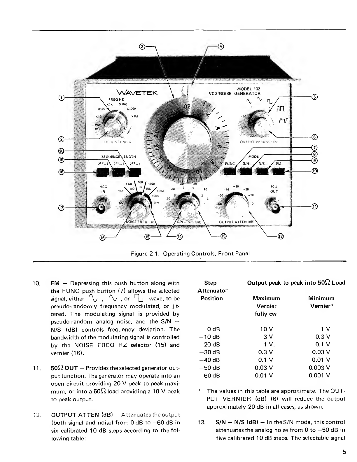
14. S/N —N/S (dB) Vernier —Allows acalibrated
fine adjustment of the S/N —N/S (dB) step at-
tenuator (13). This control is continuously vari-
able over at least a10 dB range. When added to
the coarse control (13), this amount equals the
total S/N or N/S ratio. Approximate values ot
attenuation are indicated in red numerals on the
front panel.
15, NOISE FREQ HZ —This range control selects
the clock frequency, or bandwidth for the digi-
tal, or analog noise, respectively. When using the
digital noise function, clock frequencies from
160 Hz through 1.6 MHz (indicated in black
numerals and letters on the front panel) are
available. When using analog noise or the S/N,
N/S modes, the bandwidth of the analog noise
may be selected from 10 Hz to 100 kHz (in-
dicated in red numerals and letters on the front
panel). In the FM mode, this control establishes
the bandwidth of the analog noise used for fre-
quency modulation. There are four detent posi-
tions with an overlapping vernier control (16).
With the vernier in the full cw position, the
clock frequency, or bandwidth, is equal to the
value printed to the right of the detent mark.
16, NOISE FREQ HZ Vernier —As mentioned in
number 15, this control provides acontinuous,
fine control between the detent positions of
the coarse control. When in the full cw position,
the clock frequency, or bandwidth, is equal to
the value appearing at the right of the detent
mark. As the knob is rotated ccw, the clock
frequency, or bandwidth, is decreased. In the
full ccw position, the actual value will be at
least 10:1 (and as much as 100:1) lower than
the value to the right of the detent mark.
17. VCG IN —This connector allows external volt-
age control of function generator frequency. Up
to 1000:1 frequency change may be obtained.
Apositive voltage increases frequency and a
negative voltage decreases frequency. Refer to
"Operation as aVoltage Controlled Generator.”
SEQUENCE LENGTH
18. 210 —1—Depressing this push button will
provide 1,023 counts of the selected clock fre-
quency, or bandwidth, determined by the
NOISE FREQ HZ controls (15 and 16), for
generation of adigital, or analog noise pattern.
At the end of each sequence, the pattern is
automatically repeated.
19. 215 —1—Depressing this push button will
provide 32,767 counts of the selected clock
frequency, or bandwidth, determined by the
ni/*> «or— rnr Ii~7 .._ j. I _!Anr ir* 'f..
IwikJ liU. i i z_ ouiiu uiJ tiUi iu i\Ji ,tut
generation of adigital, or analog noise pattern.
At the end of each sequence, the pattern is
automatically repeated.
20. 220 —1—Depressing this push button will
provide 1,048,575 counts of the selected clock
frequency, or bandwidth, determined by the
NOISE FREQ HZ controls (15 and 16), for
generation of adigital, or analog noise pattern.
At the end of each sequence, the pattern is
automatically repeated.
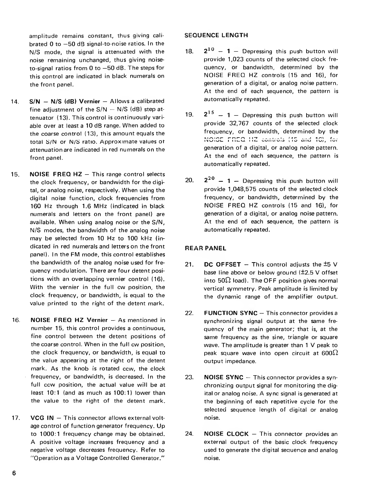
REAR PANEL
21. DC OFFSET —This control adjusts the ±5 V
base line above or below ground (±2.5 Voffset
into 50^2 load). The OFF position gives normal
vertical symmetry. Peak amplitude is limited by
the dynamic range of the amplifier output.
22. FUNCTION SYNC —This connector provides a
synchronizing signal output at the same fre-
quency of the main generator; that is, at the
same frequency as the sine, triangle or square
wave. The amplitude is greater than 1Vpeak to
peak square wave into open circuit at 600^2
output impedance.
23. NOISE SYNC —This connector provides asyn-
chronizing output signal for monitoring the dig-
ital or analog noise. Async signal is generated at
the beginning of each repetitive cycle for the
selected sequence length of digital or analog
noise.
24. NOISE CLOCK —This connector provides an
external output of the basic clock frequency
used to generate the digital sequence and analog
noise.
6