Wavetek 182A User manual

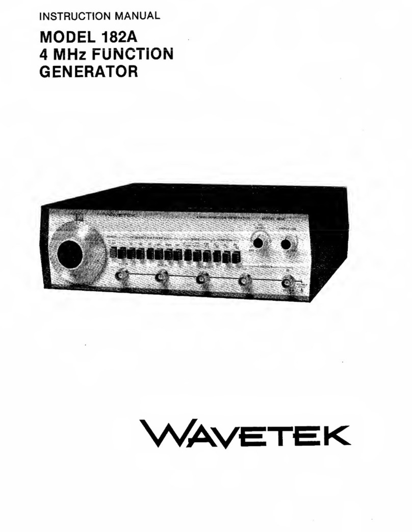
INSTRUCTION MANUAL
MODEL 182A
4MHz FUNCTION
GENERATOR
VAvetek

INSTRUCTION MANUAL
MODEL 182A
4MHz
FUNCTION GENERATOR
©-1982 -Wavetek
THIS DOCUMENT CONTAINS INFORMATION PRO-
PRIETARY TO WAVETEK AND IS SOLELY FOR IN-
STRUMENT OPERATION AND MAINTENANCE. THE
INFORMATION IN THIS DOCUMENT MAY NOT BE
DUPLICATED IN ANY MANNER WITHOUT THE
PRIOR APPROVAL IN WRITING OF WAVETEK.
V'AvETEk
WAVETEK SAN DIEGO, INC.
9045 Balboa Ave., San Diego, CA 92123
P. O. Box 85265, San Diego, CA 921 38
Tel 619/279-2200 TWX 910/335-2007 Manual Revision: 3/86

WARRANTY
Wavetek warrants that all products manufactured by Wavetek conform to published
Wavetek specifications and are free from defects in materials and workmanship for aperiod
of one (1) year from the date of delivery when used under normal operating conditions
and within the service conditions for which they were furnished.
The obligation of Wavetek arising from aWarranty claim shall be limited to repairing, or
at its option, replacing without charge, any product which in Wavetek's sole opinion proves
to be defective within the scope of the Warranty. In the event Wavetek is not able to modify,
repair or replace non-conforming defective parts or components to acondition as
warrantied within areasonable time after receipt thereof, Buyers shall be credited for their
value at the original purchase price.
Wavetek must be notified in writing of the defect or nonconformity within the Warranty
period and the affected product returned to Wavetek’s factory or to an authorized service
center within (30) days after discovery of such defect or nonconformity.
For product warranties requiring return to Wavetek, products must be returned to aservice
facility designated by Wavetek. Buyer shall prepay shipping charges, taxes, duties and
insurance for products returned to Wavetek for warranty service. Except for products
returned to Buyer from another country, Wavetek shall pay for return of products to Buyer
.
Wavetek shall have no responsibility hereunder for any defect or damage caused by
improper storage, improper installation, unauthorized modification, misuse, neglect,
inadequate maintenance, accident or for any product which has been repaired or altered
by anyone other than Wavetek or its authorized representative and not in accordance with
instructions furnished by Wavetek.
Exclusion of Other Warranties
The Warranty described above is Buyer’s sole and exclusive remedy and no other
warranty, whether written or oral, is expressed or implied. Wavetek specifically
disclaims the implied warranties of merchantability and fitness for aparticular pur-
pose. No statement, representation, agreement, or understanding, oral or written, made
by an agent, distributor, representative, or employee of Wavetek, which is not contained
in the foregoing Warranty will be binding upon Wavetek, unless made in writing and
executed by an authorized Wavetek employee. Linder no circumstances shall Wavetek
be liable for any direct, indirect, special, incidental, or consequential damages,
expenses, losses or delays (including loss of profits) based on contract, tort, or any
other legal theory.

CONTENTS
SECTION 1GENERAL DESCRIPTION
1.1 THE MODEL 182A 1-1
1.2 SPECIFICATIONS 1-1
1.2.1 Versatility 1-1
1.2.2 Frequency Precision 1-1
1.2.3 Amplitude Precision 1-1
1.2.4 Waveform Characteristics 1-2
1.2.5 General 1-2
SECTION 2INSTALLATION
2.1 MECHANICAL INSTALLATION 2-1
2.2 ELECTRICAL INSTALLATION 2-1
2.2.1 Power Connection 2-1
2.2.2 Signal Connections 2-1
2.3 ELECTRICAL ACCEPTANCE CHECK 2-1
2.4 CHANGING THE OUTPUT IMPEDANCE 2-2
SECTION 3OPERATION
3.1 CONTROLS AND CONNECTIONS 3-1
3.2 OPERATION 3-2
3.2.1 Signal Termination 3-2
3.2.2 Manual Function Generator Operation 3-2
3.2.3 Voltage Controlled Function Generator Operation 3-2
3.2.4 Waveforms 3-3
SECTION 4CIRCUIT DESCRIPTION
4.1 FUNCTIONAL BLOCK DIAGRAM ANALYSIS 4-1
SECTION 5ALIGNMENT
5.1 FACTORY REPAIR 5-1
5.2 REQUIRED TEST EQUIPMENT 5-1
5.3 REMOVING GENERATOR COVERS 5-1
5.4 ALIGNMENT 5-1
SECTION 6TROUBLESHOOTING
6.1 FACTORY REPAIR 6-1
6.2 TROUBLESHOOTING TABLES 6-1
6.3 TROUBLESHOOTING INDIVIDUAL COMPONENTS 6-1
6.3.1 Transistor 6-1
6.3.2 Diode 6-1
6.3.3 Operational Amplifier 6-1
6.3.4 FET Transistor 6-1
6.3.5 Capacitor 6-1
6.4 GENERAL INSTRUCTIONS 6-2
SECTION 7PARTS AND SCHEMATICS
iii
7.1 DRAWINGS
7.2 ORDERING PARTS
7.3 ADDENDA
7-1
7-1
7-1

SAFETY
This instrument is wired for earth grounding via the facility power wiring. Do not bypass
earth grounding with two wire extension cords, plug adapters, etc.
BEFORE PLUGGING IN the instrument, comply with installation instructions.
MAINTENANCE may require power on with the instrument covers removed. This should
be done only by qualified personnel aware of the electrical hazards.
The instrument power receptacle is connected to the instrument safety earth terminal
with agreen/yellow wire. Do not alter this connection. (Reference: @or ^stamped
inside the rear panel near the safety earth terminal.)
WARNING notes call attention to possible injury or death hazards in subsequent
operations.
CAUTION notes call attention to possible equipment damage in subsequent operations.

1.1 THE MODEL 182A
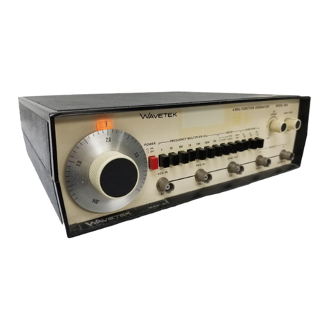
Wavetek Model 182A Four MHz Function Generator is
aprecision source of sine, triangle and square wave-
forms plus dc voltage. All are front panel variable from
0.004 Hz to 4MHz and can be externally modulated or
swept over a 1000:1 range. Output can be continuous
or the generator can be triggered or gated by an exter-
nal signal or afront panel switch. Amplitude of the
waveforms is variable from 10V peak-to-peak into 500
down to 30 mV p-p. DC reference of the waveforms
can be offset positively or negatively.
The main waveform output is 20V peak-to-peak maxi-
mum and can be varied over a30 dB range. Asecond
waveform at 2V peak-to-peak maximum (20 dB at-
tenuation) and aTTL level square at generator fre-
quency are auxiliary outputs. Inputs are provided for
external voltage controlled generator frequency (VCG)
and for triggering and gating the generator.
1.2 SPECIFICATIONS
1.2.1 Versatility
Waveforms
Sine %.triangle a, .square 1i ,TTL pulse n.
and dc.
Operational Modes
Continuous: Generator runs continuously at selected
frequency.
Triggered: Generator is quiescent until triggered by
external signal or manual trigger, then generates one
complete waveform cycle at selected frequency.
Gated: As triggered mode, except output continues
for duration of gate signal. Last waveform started is
completed.
Frequency Range
0.004 Hz to 4MHz in 7overlapping decade ranges:
xl 0.004 Hz to 4Hz
X10 0.04 Hz to 40 Hz
xl 00 0.4 Hz to 400 Hz
xIK 4Hz to 4kHz
x10K 40 Hz to 40 kHz
X100K 400 Hz to 400 kHz
x1M 4kHz to 4MHz
SECTION I
GENERAL DESCRIPTION
Function Output
%r\,1, selectable and variable to 20V p-p
(10V p-p into 50Q) HI output, and to 2V p-p (IV p-p into
50Q) LO output. Both outputs varied with a30 dB ver-
nier. Peak output current is 100 mA maximum (HI out-
put) into 500 (200 mA peak into ashort circuit). Source
impedance is 500.
DC Offset and DC Output
Waveform offset and dc output selectable and variable
thru HI and LO BNC outputs. DC output selectable by
not selecting awaveform function. HI output is ±10V
max (±5V into 500) as offset or Vdc output. Signal-
peak plus offset limited to ±10V (±5V into 500). LO
output is ±1Vmax (±0.5V into 500) as is signal-peak
plus offset limit. DC offset plus waveform attenuated
proportionately at LO (-20 dB) output.
TTL Pulse Output
TTL pulse (50% duty cycle) at generator frequency.
Drives up to 20 TTL loads.
VCG —Voltage Controlled Generator
Up to 1000:1 frequency change with external 0to
±4V signal. Upper and lower frequencies limited to
maximum and minimum of selected range.
Slew Rate: 2% of range per fts.
Linearity:
±0.5% thru X100K range; ±2% on xlM range.
Input Impedance: 2kQ.
Trigger and Gate
Input: TTL compatible levels.
Pulse Width: 50 ns minimum.
Repetition Rate: 4MHz maximum.
1.2.2 Frequency Precision
Dial Accuracy
±5% of full scale.
Time Symmetry
Square wave variation from 0.2 to 4.0 on dial less than:
±1% to 100 kHz; ±5% to 4MHz.
1.2.3 Amplitude Precision
Sine variation with frequency less than:
±0.2 dB on all ranges through X100K; ±1.0 dB to
4MHz.
1-1
1.2.4 Waveform Characteristics
Sine Distortion
Less than:
0.5% on xIK and x10K ranges; 1% on xl, X10,
x100 and x100K ranges. All harmonics 25 dB below
fundamental on x1Mrange.
Triangle Linearity
Greater than 99% to 200 kHz.
Square Wave Rise and Fall Time
At HI output, less than 50 ns for 10V p-p output into
500 termination.
1.2.5 General
Environmental
Specifications apply at 25°C ±5°C. Instrument will
operate from 0°C to 50°C ambient temperatures.
Dimensions
28.6 cm (11 'A in.) wide; 8.9 cm (3Vz in.) high; 26.7
(10'/2 in.) deep.
Weight
2.7 kg (6 lb) net; 4.5 kg (10 lb) shipping.
Power
90 to 126V or 198 to 252V (specify); 48 to 66 Hz; less
than 15watts.
NOTE
All specifications apply for dial between 0.2
and 4.0; amplitude at 10V p-p from HI out-
put into 500 termination.
1-2

SECTION Em
INSTALLATION
2.1 MECHANICAL INSTALLATION
After unpacking the instrument, visually inspect all
external parts for possible damage to connectors, sur-
face areas, etc. If damage is discovered, file aclaim
with the carrier who transported the unit. The shipping
container and packing material should be saved in
case reshipment is required.
2.2 ELECTRICAL INSTALLATION
2.2.1 Power Connection
WARNING
To preclude injury or death due to shock,
the third wire earth ground must be con-
tinuous to the facility power outlet.
Before connecting to the facility power
outlet, examine extension cords, auto-
transformers, etc., between the instru-
ment and the facility power outlet for a
continuous earth ground path. The earth
ground path can be identified at the
plug on the instrument power cord; of
the three terminals, the earth ground
terminal is the nonmatching shape,
usually cylindrical.
CAUTION
To prevent damage to the instrument,
check for proper match of line and instru-
ment voltage and proper fuse type and
rating.
NOTE
Unless otherwise specified at the time of
purchase, this instrument was shipped
from the factory for operation on a90 to
126Vac line supply and with a1/4 amp slow
blow fuse. Instruments configured for 198
to 252 Vac have a1/8 amp slow blow fuse.
Select the appropriate fuse and 115 or 230
switch position at the rear panel when
changing power sources.
2.2.2 Signal Connections
Use 3foot RG58U 500 shielded cables equipped with
female BNC connectors to distribute all input and out-
put signals.
2.3 ELECTRICAL ACCEPTANCE CHECK
This checkout procedure is ageneral verification of
generator operation. Should amalfunction be found,
refer to the warranty in the front of this manual.
Atwo channel oscilloscope, four 3foot 500 coax
cables with female BNC connectors, acoax tee con-
nector and an additional function generator are re-
quired for this procedure.
Preset the generator front panel controls as follows:
Control Position
Dial 2.0
MODE CONT (released)
FUNCTION a,
DC OFFSET OFF (ccw)
AMPLITUDE MAX (cw)
FREQUENCY MULTIPLIER X1K
Set up the oscilloscope, Model 182A and external
function generator as shown in figure 2-1 and perform
the steps in table 2-1
.
Figure 2-1. First Setup
2.4 CHANGING THE OUTPUT IMPEDANCE
The output impedance is normally:
HI 10V p-p (500 source) into 500.
LO IV p-p (500 source) into 500.
Amplitude is normally variable over 30 dB with -50 dB
lowest possible amplitude.
2-1

Figure 2-2. Second Setup
2.4 CHANGING THE OUTPUT IMPEDANCE
The output impedance is normally:
HI 10V p-p (50Q source) into 50Q.
LO IV p-p (50SJ source) into 500.
Amplitude is normally variable over 20 dB with -50 dB
lowest possible amplitude.
If simultaneous 6000 and 500 output impedances are
desired:
1.Change value of R1 48 from 4990 to 6040.
2. Remove R1 49.
The result is:
HI 10V p-p (500 source) into 500.
LO 10V p-p (6000 source) into 6000.
Amplitude is variable over 30 dB with -30 dB lowest
possible amplitude. Square wave rise and fall time is
less than 150 ns. Any value greater than 6000 may
also be substituted for the value of R1 48 for other out-
put Impedances.
To increase the range of the variable amplitude con-
trol in amodified unit beyond 30 dB, decrease the
value of R124 as necessary. Waveform quality
relative to the standard unit is not guaranteed below
-30 dB and above 20 kHz.
Table 2-1. Initial Checkout
Step Control Position/Operation Observation
1POWER ON ±10V square wave on CHI and ±IV on CH2.
Return to CHI only.
2Dial Rotate either direction. Return
to 2.0.
Rotation ccw increases frequency of Tj ;
rotation cw decreases frequency.
3FREQUENCY
MULTIPLIER Press each switch sequentially;
return to xlK. Frequency increases in decade steps, left to
right.
4AMPLITUDE Rotate ccw. Amplitude decreases.
5DC OFFSET Rotate cw. Return to OFF. Output immediately offset negative, then moves
positive. OFF return it to original level.
6AMPLITUDE Rotate cw. Square returns to original amplitude.
7Function Generator
or DC Voltage
Source
Vary input dc voltage; then discon-
nect VCG IN input.
Frequency increases with positive voltage and
decreases with negative voltage.
8FUNCTION Press A/- ,Tj ,\.Observe ,Tj ,'V waveforms.
9MODE Gate (CONT depressed, TRIG/GATE
released). Adc level near zero volts (except Tj function).
10 MANUAL TRIGGER Press and hold. Continuous A.
Set up trigger source as shown in figure 2-2. Set trigger source for 100 Hz TTL signal.
11 Agated on during positive portion of TTL
signal on CH2.
12 Trigger/Gate
i
Trigger (depressed) One -V cycle per trigger cycle.
2-2

SECTION W
OPERATION
3.1 CONTROLS AND CONNECTIONS
The generator front panel controls and connectors are
shown in figure 3-1 and keyed to the following descrip-
tions.
1Frequency Dial —Settings under the dial index
mark summed with 14 and multiplied by 3
determine the output signal frequency.
2POWER Button —Turns generator ON and OFF.
3FREQUENCY MULTIPLIER Controls -Selects
one of seven frequency multipliers for dial 1set-
ting.
4, SGenerator MODE Controls —Selects one of
the following three modes:
CONT —4released. Continuous output at
500 OUT 10 and 11 and SYNC OUT (TTL)
12 connectors.
TRIG —4and 5pressed. DC level output
until generator triggered by the MAN TRIG 6
or with asignal at the TRIG IN connector 13 .
When triggered, the generator output is one cycle
of waveform followed by adc level.
GATE —4pressed and 5released. As for
TRIG except the output is continuous for the
duration of the manual or external trigger signal.
The last cycle started is always completed.
6Manual Trigger Button —Triggers or gates the
output signals when generator mode is TRIG or
GATE (4 pressed). In trigger mode, one
waveform cycle is output when the button is
pushed. In gate mode, waveform cycles are con-
tinuously output as long as the button is held in.
7FUNCTION Selector —Selects one of three
waveforms or when all three buttons are released,
adc level.
Figure 3.1 Controls and Connectors

Impedance
8DC OFFSET Control —Offsets the 50Q OUT
waveforms or gives dc levels from -10V to
+10V (-5V to +5V into 500) at 10and from
-IV to +1V (-0.5V to +0.5V into 500) at
11 .An OFF position ensures no offset.
9AMPLITUDE Control —Ccw rotation reduces
waveform amplitudes at 10 and 11 by
30 dB. DC and offset voltages are not affected
by this control.
10 500 OUT HI Connector —The main output of
the generator at the function selected. Maximum
20V p-p (1 0V p-p into 500) with 30 dB continuous
amplitude control. 500 source impedance.
11 500 OUT LO Connector —Same as 10 ex-
cept 20 dB (1/10) lower in amplitude.
12 TTL OUT Connector —ATTL square for each
cycle of the generator. To be used for syn-
chronization or as aTTL signal capable of driv-
ing 20 TTL loads.
13 TRIG IN Connector —Accepts aTTL signal to
trigger or gate the generator. Triggers on the ris-
ing (low to high) transition and gates during the
positive (high) portion of the triggering signal.
14 VCG IN Connector —Accepts ac or dc voltages
to proportionately control frequency within the
range determined by the FREQUENCY
MULTIPLIER 3.Positive voltage increases the
frequency set by the dial 1;negative voltage
decreases the frequency. The VCG IN will not
drive the generator frequency beyond the nor-
mal dial limits of arange. Input impedance is
2kO,
3.2 OPERATION
Perform the initial checkout in Section 2for the feel of
the instrument. Any questions concerning individual
controls and connectors may be answered in
paragraph 3,1.
3.2.1 Signal Termination
Proper signal termination, or loading, of the generator
connectors is necessary for its specified operation.
For example, the proper termination of either of the
500 OUT connectors is shown in figure 3-2. Placing
the 50 ohm terminator, or 50 ohm resistance, in
parallel with ahigher impedance, matches the receiv-
ing instrument input impedance to the coax
characteristic and generator output impedance,
thereby minimizing signal reflection or power loss on
the line due to impedance mismatch.
The input and output impedances of the generator
connectors are listed below.
Connector
500 OUT (HI) 500
500 OUT (LO) 500
SYNC OUT (TTL) .. *
TRIG IN *
VCG IN 2kO
•The TTL OUT connector is diode protected and can
drive up to 20 Transistor-Transistor-Logic (TTL) loads
(low level between OV and 0.4V, and high level bet-
ween 2.4V and 5V). It should not be conencted to
resistive load less than 6000. The TRIG IN connector
accepts TTL logic levels, is diode protected, and re-
quires 500 pA drive from ahigh level output.
RECEIVING
MODEL 182AINSTRUMENT
Figure 3-2. Signal Termination
3.2.2 Manual Function Generator Operation
For basic operation, select the waveform frequency
and amplitude. The following steps demonstrate
manual control of the function generator. (Bold
numbers are keys to figure 3-1 .)
Step Control/Connector Setting
1500 OUT 10 11 Connect circuit to either
output (refer to para-
graph 3.2.1).
FREQUENCY
MULTIPLIER 3
Set to desired range of fre-
quency.
Frequency Dial 1Set to desired frequency
within the range.
FUNCTION 7
DC OFFSET 8
AMPLITUDE 9
Set to desired waveform.
Set as desired. Limit wave-
form amplitude to prevent
clipping (see figure 3-3).
Select for desired ampli-
tude.
3-2

3.2.3 Voltage Controlled Function Generator
Operation
four times the multiplier setting, and the
lower limit is 1/1 000th of the upper limit.
Operation as avoltage controlled function generator
(VCG) is as for amanually controlled function
generator, only the frequency within particular ranges
is additionally controlled by an external voltage (±4V
excursions) injected at the VCG IN connector. Per-
form the steps given in paragraph 3.2.2, only set the
frequency dial to determine areference from which
the frequency is to be voltage controlled.
oDC
OFFSET
DC OFFSET
EXCESSIVE
POSITIVE
OFFSET OR
LOADING
NEGATIVE
DC OFFSET
EXCESSIVE
NEGATIVE
OFFSET OR
LOADING
OUTPUT
MAIN DIAL VCG IN FREQUENCY
SETTING VOLTAGE FACTOR
T-4-1
—3-
-2-
EXAMPLE 1
1
//////
-
2.0
-
.V--
3.0- Ns
4.0-
Figure 3-4. VCG Voltage-to-Frequency Nomograph
The up to 1000:1 VCG sweep of the generator fre-
quencies available in each range results from a4V ex-
cursion at the VCG IN connector. With the frequency
dial set to 4.0, excursions between —4V and 0V at
VCG IN provide the up to 1000:1 frequency sweep.
With the dial set to .004, excursions between 0V and
+4V at VCG IN provide the up to 1000:1 sweep within
the set frequency range.
Figure 3-3. DC OFFSET Control 3.2.4 Waveforms
1.For frequency control with positive dc inputs at
VCG IN, set the dial for alower frequency limit.
See figure 3-5 for definition of controllable waveform
characteristics.
2. For frequency control with negative dc inputs at
VCG IN, set the dial for an upper frequency limit.
3. For modulation with an ac input at VCG IN, set
the dial at the desired center frequency. Do not
exceed the maximum dial range of the selected
frequency range.
Figure 3-4 is anomograph with examples of dial and
voltage effects. Example 1shows that with 0V VCG in-
put, frequency is determined by the main dial setting,
2in this example. Example 2shows that with a
positive VCG input, output frequency is increased. Ex-
ample 3shows that with anegative VCG input, output
frequency is decreased. (Note that the Output Fre-
quency Factor column value must be multiplied by a
frequency range multiplier to give the actual output
frequency.)
NOTE
Nonlinear operation may result when the
VCG input voltage is excessive; that is,
when the attempted generator frequency
exceeds the range limits. The upper limit is
(iff)
0Vdc PERI0D
CONTINUOUS
MODE
1
OFFSET
SINE^
AMPLITUDE
.1
TRIGGERED
MODE '
^fvAAAAAA/
^triangleA^vXAAAA/V
squareIJHJIJTJIJTJIJIJ
SYNCXJTjn_nJT_n—n_TLT
TRIG m’ZUZZZZZZZZZZZZUZZZ
SINE—%V-
SQUARE U"~
-^v
TT
TRIG IN- TZ2_
SINE WV V'
MODE ^TRIANGLE VVV ^
SQUARE
|_J [_J 1_J Ul
Figure 3-5. Waveform Characteristics
3-3

4-0

SECTION “
CIRCUIT DESCRIPTION
4.1 FUNCTIONAL BLOCK DIAGRAM ANALYSIS
This section describes the functions of major circuit
elements and their relationships to one another as
shown in figure 4-1 ,functional block diagram. The fol-
lowing sections in this manual provide more detailed
information for maintaining the instrument.
As shown in figure 4-1 ,the VCG sums voltage inputs
from the frequency dial and the VCG IN connector.
This sum voltage controls the magnitude of acomple-
mentary current source and current sink. This current
varies linearily from approximately 2mA to 2/iA and
over the 1000:1 (4.0 to .004) range of each frequency
multiplier. The VCG also controls the trigger baseline
compensation circuit, which consists of another cur-
rent sink at twice the current magnitude.
The diode gate, controlled by the comparator output,
connects either the current source or the current sink
to the timing capacitor selected by the frequency
multiplier. When the current source is switched in, the
charge on the timing capacitor will rise linearily, pro-
ducing the positive-going triangle slope. Likewise, the
current sink produces the negative-going triangle
slope.
The triangle amplifier is aunity gain amplifier whose
output is fed to the comparator and to the output cir-
cuits. The comparator operates as awindow detector
with limit points set to the triangle peaks. The ±2V
output is sent back to the diode gate and to the output
circuits. When the output is +2V, the triangle is
positive-going until the +1.25V limit is reached and
the comparator output switches to -2V. When the
output is -2V, the triangle is negative-going until the
-1,25V limit is reached and the comparator output
switches back to +2V, repeating the process. In this
manner, the basic function generator loop, the bold
path in figure 4-1, produces simultaneous generation
of triangle and square waves at the same frequency.
The output frequency is determined by the magnitude
of the timing capacitor selected by the frequency
multiplier switches and by the magnitude of the cur-
rents supplied to and removed from it. Since the cur-
rents are linearily proportional to the sum of the VCG
inputs, so will be the output frequency.
To extend the lower frequency capability of the
generator, acapacitance multiplier circuit divides
VCG currents by 10 (effectively multiplying the timing
capacitor by 10) for each of the lower 3multiplier
ranges.
The TTL square from one side of the comparator is
buffered and sent to the SYNC OUT TTL connector.
The other side is sent to the trigger flip-flop and to a
level shifter to produce the ±2V bipolar square for
the diode gate and the square shaper circuits. The
square shaper converts the square into acurrent
signal and applies it to the Tj FUNCTION switch.
The buffered triangle is applied to the \FUNCTION
switch and to the sine converter input. The sine con-
verter, using the nonlinear characteristics of its
diodes, converts the triangle into asinusoidal current
for the %FUNCTION switch.
The selected function is sent to the preamplifier,
where it is inverted and buffered. The preamplifier out-
put goes to the output amplifier through the
AMPLITUDE control where it is summed with offset
voltage from the DC OFFSET control. Here, waveform
and offset are inverted and amplified to a10V peak
signal which can drive a500 termination from a500
source impedance. The output amplifier drives the
500 OUT HI connector and aresistor divider produc-
ing the 500 OUT LO output.
Noncontinuous modes of operation (trigger and gate)
result from allowing or preventing the VCG current
source from charging the timing capacitor. Whenever
the trigger flip-flop output is low, each of the two trig-
ger diodes conduct acurrent I, sourcing 21 to the
baseline compensation circuit. This removes the cur-
rent Ifrom the VCG current source and forces a0V
baseline at the triangle amplifier input.
When the CONT switch is released, trigger logic is in-
hibited from passing any trigger signals and the trig-
ger flip-flop output is held high. This prevents the trig-
ger diodes from conducting and the generator loop
operates continuously.
When the CONT switch is pressed, the generator loop
is held at the 0V baseline. Pressing the TRIG/GATE
TRIG/GATE switch puts the instrument in triggered
mode and any external or manual trigger signals at
the trigger logic input will be transformed into anar-
row pulse corresponding to the low-to-high transition
of the trigger input. This pulse sets the trigger flip-flop
high and allows the generator loop to run. When the
triangle negative peak is reached, the comparator
low-to-high transition clocks the trigger flip-flop low

and, when the OV baseline level is reached, the
generator loop again stops. The result is asingle
waveform generated after the triggering signal cor-
responding to 0to 36€° of phase. Successive trig-
gered waveforms always start at the same 0° point.
Releasing the TRIG/GATE switch puts the instrument
in the gated mode. This is identical to the triggered
mode, except the trigger flip-flop is held high for the
full duration of the triggering signal. The generator
produces continuous waveforms during the time the
external signal is high or the manual trigger switch is
held in. The last triggered cycle started is always com-
pleted and successive gated bursts always start at the
0° point.
4-2

5
SECTION
ALIGNMENT
5.1 FACTORY REPAIR
Wavetek maintains afactory repair department for those
customers not possessing the necessary personnel or
test equipment to maintain the instrument. If an instru-
ment is returned to the factory for alignment or repair,
adetailed description of the specific problem should be
attached to minimize turnaround time.
5.2 REQUIRED TEST EQUIPMENT
VoltmeterMicrovolt dc measurement (1 %accuracy)
Oscilloscope >60 MHz bandwidth
Counter 4MHz (0.1% accuracy)
50Q Feedthru ±1%accuracy, 2W
Distortion Analyzer To 400 kHz
RG58U Coax Cable ... 3ft length BNC male contacts
5.3 REMOVING GENERATOR COVERS
1.Invert the instrument and remove the four screws
in the bottom cover.
2. Turn the instrument upright; remove the top cover
for access to generator alignment controls.
3. When alignment is complete, secure the bottom
cover with four screws.
NOTE
Remove the cover only when it is necessary
to make adjustments or measurements.
5.4
ALIGNMENT
After referring to the following preliminary data, perform
alignment, as necessary, per table 5-1 .If performing par-
tial alignment, check previous settings and adjustments
for applicability. See figure 5-1 for alignment control
location.
The completion of these calibration procedures returns
the instrument to correct calibration. All limits and
tolerances given in these procedures are calibration
guides and should not be interpreted as instrument
specifications. Instrument specifications are given in
section 1of this manual.
1.All measurements made at the FUNCTION OUTcon-
nector must be terminated into a50Q(± 1%)load.
2. Start the alignment by connecting the unit to an
appropriate ac power source and setting the front
panel switches as follows:
POWER ON
Frequency Dial 4.0
FREQ MULT (Hz) XIK
MODE CONT
FUNCTION ...
DC OFFSET OFF
AMPLITUDE MAX
3.
Allow the unit to warm up at least 30 minutes for final
alignment. Keep the instrument cover on to main-
tain heat. Remove cover only to make adjustments
or measurements.
Table 5-1. Alignment Procedure
Step Check Tester
Test
Point Control Setting Adjust Result Remark
1Power
Supply
Voltmeter C4 +Paragraph 5.4, Step 2+15 ±.75V Verify.
±15V should track
within 30 mV
2C5 --15 ±.75V
3C7 + + 5±.25V
4C6 --5 ±.25V
5Capacitor
Multiplier
Zero
SW3 -B
Wiper R90 0±2 mV
5-1

Table 5-1. Alignment Procedure (Continued)
Step Check Tester Test
Point
Control
Setting Adjust Result Remark
6Approximate
Bottom of
the Dial
Frequency
Counter 50fi OUT
HI (termin-
ate into
50fl
Dial: .004
FREQ MULT: 10K R37 20 ms
period
-> Bottom
of the
Dial
Symmetry
Scope R49 Equalize (+)
and (-) half
cycles
Set scope to (-) trigger;
display one full cycle.
Align positive transition to
center of screen. Multiply the
horizontal display xlO. Set
scope (+)trigger; adjust R49
to align negative transition
with center of screen
8Bottom of
the Dial
Frequency
Counter FREQ MULT: xlK R37 350 ±50 ms
period
9Top of the
Dial
Symmetry
Scope Dial: 4.0 R45 Equalize (+)
and (-) half
cycles
See step 7
10 Top of the
Dial
Frequency
Counter Dial: 4.0
FREQ MULT: XlK R19 4±0.2 kHz
11 FREQ MULT: xlOK 40 ±.8 kHz Verify
12 FREQ MULT: xlM C34 4±.02 MHz
13 FREQ MULT: x100K 400 ±8 kHz Verify.
If necessary, trim by
changing value of C33
14 FREQ MULT: x100 R86 2.5 ±.05 ms
15 FREQ MULT: x10 25 ±.5 ms Verify
16 FREQ: X
1
250 ±5ms
17 Sine
Distortion
Distortion
Analyzer
FUNCTION: %
FREQ MULT: xlK R97
R114 Adjust for
minimum
distortion
It may be necessary
to reduce amplitude
to 5V peak
18 Output
Amplitude Scope FUNCTION: \R118 10 Vp-p +.3V
-ov
19 Output
Offset
Voltmeter FUNCTION: %R112 0V ±50 mv
20 Baseline
Zero Scope MODE: Trigger R81 0V ±75 mv It may be necessary
to trim the baseline
with R80
5-2

A
/ \
I\
\/
vy
TRIGGER LOGIC
-C27- J, |
J-C26-
-+5V- —-R74—
J
DIG COM
--DISTORTION
i‘
c> o
E25 £E2t
is 5
ti.
12 SB
o
010PUT COM
Jj_iiiii%~~r z
J—15V- &cd .U13 *5I-I
+15V-J _r5124- —i—
-COM- /I \I1
J/I-cs-\jIJ
n7.in
-CM—, SRp I11
R123
OUTPUT 1
SINE; OFFSET",
I'f ton. tod1;it ii7°Df-
O', -?.°°7FREQi AF"!.°
.DISTORTION'S^'
||—RT32—
•n Q14
Q
**001-iIM-cra-
'OUTPUThJ-7" ft
FREQ ^mBASELINE
£1--1V"-11-
^-R97 l
-C47- —Rltn— -R137-
-CR22-W
rr\
f
!+W cap multiplier""
ICAPACITANCE Ml ZERO§
1*
33
—
-MR- 1
SW1 3W2 SW3 SW4 I
is e,Q1V7~v\ g'rs*
[*? JI((_), |))
ijawecowvEmiBJj'-il!—J-
SW7 SIW ISUB SWiT ~SWl~n SW12 SW13 SWH —CSS—-R1M-
SW15 "C58'J|_ |
Figure 5-1. Alignment Locations
Tm>

SECTION U
TROUBLESHOOTING
6.1 FACTORY REPAIR
Wavetek maintains afactory repair department for
those customers not possessing the necessary per-
sonnel or test equipment to maintain the instrument. If
an instrument is returned to the factory for alignment
or repair, adetailed description of the specific prob-
lem should be attached to minimize turnaround time.
6.2 TROUBLESHOOTING TABLES
Table 6-1 gives an index of the troubleshooting tables
by indications of common problems. The tables do not
cover every possible trouble, but, when used in con-
junction with circuit descriptions and schematics, will
be an aid in systematically isolating faulty components.
6.3 TROUBLESHOOTING INDIVIDUAL
COMPONENTS
6.3.1 Transistor
1.Atransistor is defective if more than one volt is
measured across its base-emitter junction in the
forward direction.
2. Atransistor when used as aswitch may have a
few volts reverse bias voltage across base-
emitter junction.
3. If the collector and emitter voltages are the
same, but the base emitter voltage is less than
500 mV forward voltage (or reversed bias), the
transistor is defective.
4. Atransistor is defective if its base current is
larger than 10% of its emitter current (calculate
currents from voltage across the base and emit-
ter series resistors).
5. In atransistor differential pair (common emitter
stages), either their base voltages are the same
in normal operating condition, or the one 'with
less forward voltage across its base emitter
junction should be off (no collector current);
otherwise, one of the transistors is defective.
6.3.2 Diode
Adiode (except azener) is defective if there is greater
than one volt (typically 0.7 volt) forward voltage
across it.
6.3.3 Operational Amplifier
1. The “+”and inputs of an operational
amplifier will have less than 15 mV voltage dif-
ference when operating under normal conditions.
2. When the output of the amplifier is connected to
the “—”input (voltage follower connection), the
output should be the same voltage as the “+”
input voltage; otherwise, the operational ampli-
fier is defective.
3. If the output voltage stays at maximum positive,
the “+”input voltage should be more positive
than the "—”input voltage, or vice versa; other-
wise, the operational amplifier is defective.
6.3.4 FET Transistor
1.No gate current should be drawn by the gate of
an FET transistor. If so, the transistor is defective.
2. The gate-to-source voltage is always reverse
biased under anormal operating condition;
e.g., the source voltage is more positive than the
gate voltage for 2N5485, and the source voltage
is more negative than gate voltage for a2N5462.
Otherwise, the FET is defective.
3. If the device supplying gate voltage to an FET
saturates, the FET has too large aVgs (pinch off)
for the circuit and should be replaced.
6.3.5 Capacitor
1.Shorted capacitors have zero volts across their
terminals.
2. Opened capacitor can be located (but not always)
by using agood capacitor connected in parallel
with the capacitor under test and observing the
resulting effect.
6-1

6.4 GENERAL INSTRUCTIONS
When encountering aproblem, it is advisable to return
as many of the front panel controls as possible to their
initial settings and still retain the problem. The trouble-
shooting tables in this section generally begin at these
initial settings and specify all subsequent setups.
Preset the front panel controls as follows.
Control Position
Frequency Dial 4.0
POWER ON
FREQ MULT (Hz) IK
FUNCTION 1j
DC OFFSET OFF
AMPLITUDE MAX
CAUTION
To prevent damage to components, turn
unit off while removing or replacing
components, connectors or pc boards.
The Suspected malfunctioning condition should be
double checked to eliminate the possibility of improper
settings or connections. Before attempting fault isola-
tion, the unit should be checked for proper line
voltage selection (refer to Section 2). Agood visual in-
spection of the boards and chassis wires for damage
or overheating often saves much time.
Once the malfunction is defined, begin the isolation
procedure by selecting an indication in table 6-f
which best describes the malfunction and proceed to
the referenced troubleshooting table.
Follow through the checks in the troubleshooting table,
using schematics and assemblies as aguide. When
positive results are not obtained, perform the in-
dicated corrective procedure.
Table 6-1. Fault Isolation
Indication Table
1.Fuse blown, no power indication or no
outputs. 6-2
2. Function outputs missing or clipped
when TTL sync OK. Triangle problem.
6-3
3. Sine waveform problem. 6-4
4. Square waveform problem. 6-5
5. TTL sync output problem. 6-6
6. Generator frequency does not respond
correctly to dial and VCG input.
6-7
7. Waveform symmetry problem. 6-8
8. Problem on bottom three ranges only. 6-9
9. Generator trigger and gate mode prob-
lem.
6-10
Table 6-2. Power Supplies and Generator Loop
Indication: Fuse blown, no power indication or no outputs.
Check If Faulty, Check
1.Set all controls in their initial positions (refer to paragraph 6.4).
2. Ensure line voltage matches instrument configuration (refer to Section 2).
Check fuse.
Replace fuse; check for nor-
mal operation.
3. Check Cl (+)and C2 (-) for ±20 to 26V unregulated dc.
4. Check indicator lamp.
5. Check C4( +)for +15 Vdc.
6. Check C5 (-)for -15Vdc.
a. CR1 -CR4.
b. C1,C2.
c. SW1.
d. T1, RV1, FI (bracket as-
sembly).
DS1 and VR2, wiring E34
and E33.
a. VR1.
b. Excessive loading; use
board jumpers to isolate
cause.
a. Q2.
b. U2.Q1.
c. Excessive loading; use
board jumpers to isolate
cause.
6-2
Other manuals for 182A
2
Table of contents
Other Wavetek Portable Generator manuals

Wavetek
Wavetek 1001A User manual

Wavetek
Wavetek 150 User manual

Wavetek
Wavetek 188 User manual

Wavetek
Wavetek 144 User manual

Wavetek
Wavetek 180 User manual

Wavetek
Wavetek 188 User manual

Wavetek
Wavetek 182A User manual

Wavetek
Wavetek 182A User manual

Wavetek
Wavetek 1001A User manual

Wavetek
Wavetek 132 User manual
Popular Portable Generator manuals by other brands

Daewoo
Daewoo DAIG Series user manual

Arvey
Arvey A1 User manual and warranty statement

HERON
HERON 8896431 Translation of the original user manual

Klein Tools
Klein Tools KTB1000 instruction manual

Bohmer-AG
Bohmer-AG W Series Operation manual

Brightwin Electronics
Brightwin Electronics BRT LB02G quick start guide