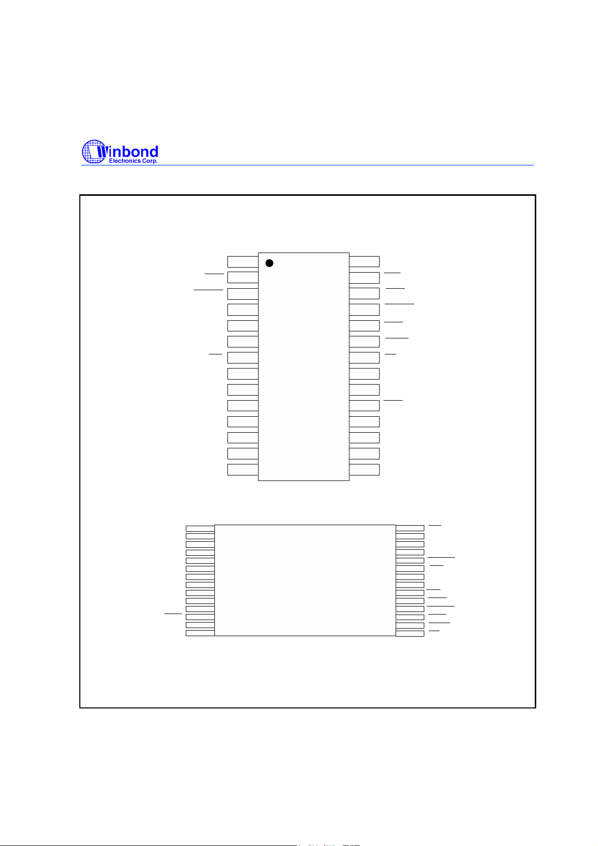
Winbond ISD1700 Series User manual

PRELIMINARY
Publication Release Date: February 7, 2006
Revision 1.2
ISD1700
Series
Multi-Message
Single-Chip
Voice Record & Playback Devices

ISD1700 SERIES
- 2 -
TABLE OF CONTENTS
1GENERAL DESCRIPTION ..............................................................................................................5
2FEATURES......................................................................................................................................6
3BLOCK DIAGRAM...........................................................................................................................7
4PINOUT CONFIGURATION............................................................................................................8
5PIN DESCRIPTION .........................................................................................................................9
6FUNCTIONAL DESCRIPTION ......................................................................................................13
6.1 Detailed Description...............................................................................................................13
6.1.1 Audio Quality ...............................................................................................................13
6.1.2 Message Duration........................................................................................................13
6.1.3 Flash Storage ..............................................................................................................13
6.2 Memory Array Architecture ....................................................................................................13
6.3 Modes of Operations..............................................................................................................14
6.3.1 Standalone (Push-Button) Mode .................................................................................14
6.3.2 SPI Mode .....................................................................................................................14
7ANALOG PATH CONFIGURATION (APC)...................................................................................15
7.1 APC Register .........................................................................................................................15
7.2 Device Analog Path Configurations .......................................................................................16
8STANDALONE (PUSH-BUTTON) OPERATIONS ........................................................................17
8.1 Operation Overview ...............................................................................................................17
8.1.1 Record Operation ........................................................................................................17
8.1.2 Playback Operation .....................................................................................................18
8.1.3 Forward Operation.......................................................................................................18
8.1.4 Erase Operation...........................................................................................................19
8.1.5 Reset Operation...........................................................................................................21
8.1.6 VOL Operation.............................................................................................................21
8.1.7 FT (Feed-Through) Operation .....................................................................................21
8.2 vAlert Feature (Optional)........................................................................................................21
8.3 Sound Effect (SE) Editing ......................................................................................................21
8.3.1 Sound Effects (SEs) ....................................................................................................21
8.3.2 Entering SE Mode........................................................................................................22
8.3.3 SE Editing ....................................................................................................................22
8.3.4 Exiting SE Mode ..........................................................................................................22
8.3.5 Sound Effect Duration..................................................................................................22
8.4 Analog Inputs .........................................................................................................................22

ISD1700 SERIES
Publication Release Date: February 7, 2006
- 3 - Revision 1.2
8.4.1 Microphone Input .........................................................................................................23
8.4.2 AnaIn Input...................................................................................................................23
9CIRCULAR MEMORY MANAGEMENT ........................................................................................24
9.1 Restoring Circular Memory Architecture................................................................................26
10 SERIAL PERIPHERAL INTERFACE (SPI) MODE .......................................................................27
10.1 Microcontroller Interface ........................................................................................................27
10.2 SPI Interface Overview ..........................................................................................................27
10.2.1SPI Transaction Format...............................................................................................27
10.2.2MOSI Data Format.......................................................................................................28
10.2.3MISO Data Format.......................................................................................................29
10.3 SPI Command Overview........................................................................................................30
10.4 Switching from SPI mode to Standalone Mode .....................................................................31
10.5 ISD1700 Device Registers.....................................................................................................31
10.5.1Status Register 0 (SR0)...............................................................................................32
10.5.2Status Register 1 (SR1)...............................................................................................33
10.5.3APC Register ...............................................................................................................33
10.5.4Play Pointer..................................................................................................................33
10.5.5Record Pointer.............................................................................................................34
10.5.6DEVICEID Register .....................................................................................................34
11 SPI COMMAND REFERENCE......................................................................................................35
11.1 SPI Priority Commands..........................................................................................................36
11.1.1PU Power Up (0x01)....................................................................................................36
11.1.2STOP (0x02)................................................................................................................37
11.1.3RESET (0x03)..............................................................................................................37
11.1.4CLR_INT(0x04)............................................................................................................37
11.1.5RD_STATUS (0x05) ....................................................................................................38
11.1.6PD (0x07) Power Down ...............................................................................................38
11.1.7DEVID (0x09) Read Device ID ....................................................................................39
11.2 Circular Memory Commands .................................................................................................39
11.2.1PLAY (0x40) ................................................................................................................39
11.2.2REC (0x41) ..................................................................................................................40
11.2.3ERASE (0x42) .............................................................................................................40
11.2.4G_ERASE (0x43) Global Erase...................................................................................40
11.2.5FWD (0x48) .................................................................................................................41
11.2.6CHK_MEM (0x49) Check Circular Memory.................................................................41

ISD1700 SERIES
- 4 -
11.2.7RD_PLAY_PTR (0x06) ................................................................................................42
11.2.8RD_REC_PTR (0x08)..................................................................................................42
11.3 Analog Configuration Commands..........................................................................................42
11.3.1RD_APC (0x44) Read APC Register ..........................................................................42
11.3.2WR_APC1 (0x45) Load APC Register ........................................................................43
11.3.3WR_APC2 (0x65) Load APC Register ........................................................................43
11.3.4WR_NVCFG (0x46) Write APC to Non-Volatile Memory ............................................44
11.3.5LD_NVCFG (0x47) Load APC register from Non-Volatile Memory.............................44
11.4 Direct Memory Access Commands .......................................................................................44
11.4.1SET PLAY (0x80) ........................................................................................................45
11.4.2SET_REC (0x81) .........................................................................................................45
11.4.3SET_ERASE (0x82) ....................................................................................................46
11.5 Additional Command..............................................................................................................46
12 TIMING DIAGRAMS ......................................................................................................................47
12.1 Record, play and erase..........................................................................................................47
13 ABSOLUTE MAXIMUM RATINGS ................................................................................................51
13.1 Operating Conditions .............................................................................................................52
14 ELECTRICAL CHARACTERISTICS .............................................................................................53
14.1 DC Parameters ......................................................................................................................53
14.2 AC Parameters.......................................................................................................................54
15 TYPICAL APPLICATION CIRCUITS.............................................................................................55
15.1 Good Audio Design Practices................................................................................................58
16 PACKAGING .................................................................................................................................59
16.1 28-Lead 8x13.4mm Plastic Thin Small Outline Package (TSOP) Type 1 - IQC....................59
16.2 28-Lead 300-Mil Plastic Small Outline Integrated Circuit (SOIC)..........................................60
16.3 28-Lead 600-Mil Plastic Dual Inline Package (PDIP) ............................................................61
16.4 Die Information.......................................................................................................................61
17 ORDERING INFORMATION .........................................................................................................62
18 VERSION HISTORY......................................................................................................................63

ISD1700 SERIES
Publication Release Date: February 7, 2006
- 5 - Revision 1.2
1 GENERAL DESCRIPTION
The Winbond®ISD1700 ChipCorder®Series is a high quality, fully integrated, single-chip multi-
message voice record and playback device ideally suited to a variety of electronic systems. The
message duration is user selectable in ranges from 26 seconds to 120 seconds, depending on the
specific device. The sampling frequency of each device can also be adjusted from 4 kHz to 12 kHz
with an external resistor, giving the user greater flexibility in duration versus recording quality for each
application. Operating voltage spans a range from 2.4 V to 5.5 V to ensure that the ISD1700 devices
are optimized for a wide range of battery or line-powered applications.
The ISD1700 is designed for operation in either standalone or microcontroller (SPI) mode. The device
incorporates a proprietary message management system that allows the chip to self-manage address
locations for multiple messages. This unique feature provides sophisticated messaging flexibility in a
simple push-button environment. The devices include an on-chip oscillator (with external resistor
control), microphone preamplifier with Automatic Gain Control (AGC), an auxiliary analog input, anti-
aliasing filter, Multi-Level Storage (MLS) array, smoothing filter, volume control, Pulse Width
Modulation (PWM) Class D speaker driver, and current output.
The ISD1700 devices also support an optional “vAlert” (voiceAlert) feature that can be used as a new
message indicator. With vAlert, the IC strobes an external LED to indicate that a new message is
present. Four special sound effect locations are reserved for audio confirmation of commands, such as
“Start Record”, “Stop Record,” and “Erase.”
Recordings are stored in on-chip Flash memory cells, providing zero-power message storage. This
unique single-chip solution is made possible through Winbond’s patented Multi-Level Storage (MLS)
technology. Audio data are stored directly in solid-state memory without digital compression, providing
superior quality voice and music reproduction.
Voice signals can be fed into the chip through two independent paths: a differential microphone input
and a single-ended analog input. For outputs, the ISD1700 provides a Pulse Width Modulation (PWM)
Class D speaker driver and a separate analog output simultaneously. The PWM can directly drive a
standard 8Ωspeaker or typical buzzer, while the separate analog output can be configured as a
single-ended current or voltage output to drive an external amplifier.
The ISD1700 devices automatically enter into power down mode for power conservation when an
operation is completed.
In the SPI mode, the user has full control via the serial interface in operating the device. This includes
random access to any location inside the memory array by specifying the start address and end
address of operations. SPI mode also allows access to the Analog Path Configuration (APC) register.
This register allows flexible configuration of audio paths, inputs, outputs and mixing. The APC default
configuration for standalone mode can also be modified by storing the APC to a non-volatile register
(NVCFG) that is loaded at initialization. Utilizing the capabilities of ISD1700 Series, designers have
the control and flexibility to implement high-end products.
Notice: The specifications are subject to change without notice. Please contact Winbond Sales Offices or
Representatives to verify current or future specifications. Also refer to the website for any related application notes.

ISD1700 SERIES
- 6 -
2 FEATURES
Integrated message management systems for single-chip, push-button applications
oREC :level-trigger for recording
oPLA
Y
:edge-trigger for individual message or level-trigger for sequential playback
oERASE:edge-triggered erase for first or last message or level-triggered erase for all messages
oFWD :edge-trigger to advance to the next message or fast message scan during the playback
oVOL : 8 levels output volume control
oINTRDY : ready or busy status indication
oRESET : bring back to the default state
oAutomatic power-down after each operation cycle
Selectable sampling frequency controlled by an external oscillator resistor
Sampling Frequency 12 kHz 8 kHz 6.4 kHz 5.3 kHz 4 kHz
Rosc 60 kΩ80 kΩ100 kΩ120 kΩ160 kΩ
Selectable message duration
oA wide range selection from 30 secs to 240 secs at 8 kHz sampling frequency
Message and operation indicators
oFour customizable Sound Effects (SE) for audible indications
oOptional vAlert (voiceAlert) to indicate the presence of new messages
oLED: stay on during recording, blink during playback, forward and erase operations
Dual operating modes
oStandalone mode:
Integrated message management techniques
Automatic power-down after each operation cycle
oSPI mode:
Fully user selectable and controllable options via Analog Path Configuration (APC) register
Two individual input channels
oMIC+/MIC-: differential microphone inputs with AGC (Automatic Gain Control)
oAnaIn: single-ended auxiliary analog input for recording or feed-through
Dual output channels
oPWM Class D speaker amplifier to directly drive an 8 Ωspeaker or a typical buzzer
oConfigurable AUD (current) or AUX (voltage) single-ended output drive external power amplifier
ChipCorder standard features
oHigh-quality, natural voice and audio reproduction
o2.4V to 5.5V operating voltage
o100-year message retention (typical)
o100,000 record cycles (typical)
Temperature options:
oCommercial: 0°C to +50°C (die); 0°C to +70°C (packaged units)
oIndustrial: -40°C to +85°C (packaged units)
Package options: Lead-free packaged units
Package types: available in die, PDIP, SOIC and TSOP

ISD1700 SERIES
Publication Release Date: February 7, 2006
- 7 - Revision 1.2
3 BLOCK DIAGRAM
Internal
Clock Timing
Nonvolatile
Multi-Level Storage
Array
Power Conditioning
Automatic
Gain Control
Anti-
Aliasing
Filter Smoothing
Filter
Sampling
Clock
SP+
SP-
V
CCA
AGC
MIC-
MIC+
R
OSC
AUD /
AUX
Amp
V
CCD
V
SSD
Device Control
V
SSA
V
SSP1
V
CCP
SPI Interface
MISOMOSISCLKSSREC PLAY ERASE FT
Volume
Control
AnaIn
Amp
MUX
AGC
Amp
AnaIn
Amp
V
SSP2
FWD VOL LEDINT/RDYRESET

ISD1700 SERIES
- 8 -
4 PINOUT CONFIGURATION
SOIC / PDIP
ISD1700
VCCD
PLAY
RESET
INT / RDY
FWD
VSSA
FT
LED
28
27
26
25
24
23
22
MIC-
MIC+
VCCA
21
SP-
ERASE
1
2
3
4
5
6
7
8
9
10
11
12
13
14
20
19
18
17
16
15
REC
MOSI
SS
SCLK
MISO
AnaIn
VSSP2
VCCP
VSSP1
Sp+
AUD / AUX
AGC
VOL
ROSC
VSSD
TSOP
ISD1700
VSSA
MIC-
MIC+
SP-
1
2
3
4
5
6
7
8
9
10
11
12
13
14
AnaIn
VSSP2
VCCP
VCCA
VSSP1
Sp+
AUD/AUX
AGC
ROSC
VOL
VCCD
MOSI
SCLK
MISO
INT / RDY
28
27
26
25
24
23
22
21
20
19
18
17
16
15
REC
VSSD
LED
RESET
SS
FT
PLAY
ERASE
FWD

ISD1700 SERIES
Publication Release Date: February 7, 2006
- 9 - Revision 1.2
5 PIN DESCRIPTION
PIN
NAME PDIP /
SOIC TSOP FUNCTIONS
VCCD 1 22
Digital Power Supply: It is important to have a separate path for each
power signal including VCCD, VCCA and VCCP to minimize the noise
coupling. Decoupling capacitors should be as close to the device as
possible.
LED 2 23
LED: This output turns on an LED during a record cycle and blinks LED
during playback, forward and erase operations.
RESET 3 24
RESET: When Low, the device enters into a known state and initializes all
pointers to the default state. This pin has an internal pull-up resistor [1].
MISO 4 25 Master In Slave Out: The I1700 places data on the MISO line one half-
cycle before the falling edge of SCLK. Data is shifted out on the falling
edge of SCLK. When the SPI is inactive ( SS = high) , it’s tri-state.
MOSI 5 26
Master Out Slave In: Data input of the SPI interface when the device is
configured as slave. The master microcontroller places data on the MOSI
line one half-cycle before the rising edge of SCLK. Data is latched into the
device on the rising edge of SCLK. When not used, it should be tied High.
SCLK 6 27
Serial Clock: Clock of the SPI interface. It is usually generated by the
master device (typically microcontroller) and is used to synchronize the
data transfer in and out of the device through the MOSI and MISO lines,
respectively. When not used, it should be tied High.
SS 7 28
Slave Select: This input, when low, selects the device as slave device
and enables the SPI interface. When not used, it should be tied High.
VSSA 8 1
Analog Ground: It is important to have a separate path for each ground
signal including VSSA, VSSD, VSSP1 and VSSP2 to minimize the noise
coupling.
AnaIn
9 2
AnaIn: Auxiliary analog input to the device for recording or feed-through.
An AC-coupling capacitor (typical 0.1uF) is necessary and the amplitude
of the input signal should not exceed 1.0 Vpp. Depending upon the D3 of
APC register, AnaIn signal can be directly recorded into the memory,
mixed with the Mic signal then recorded into the memory or buffered to
the speaker and AUD/AUX outputs via feed-through path.
MIC+ 10 3
MIC+: Non-inverting input of the differential microphone signal. The input
signal should be AC-coupled to this pin via a series capacitor. The
capacitor value, together with an internal 10 KΩresistance on this pin,
determines the low-frequency cutoff for the pass band filter. The Mic
analog path is also controlled by D4 of APC register.
MIC- 11 4
MIC-: Inverting input of the differential microphone signal. The input signal
should be AC-coupled to the MIC+ pin. It provides input noise-
cancellation, or common-mode rejection, when the microphone is
connected differentially to the device. The Mic analog path is also
controlled by D4 of APC register.

ISD1700 SERIES
- 10 -
PIN
NAME PDIP /
SOIC TSOP FUNCTIONS
VSSP2 12 5
Ground for Negative PWM Speaker Driver: It is important to have a
separate path for each ground signal including VSSA, VSSD, VSSP1 and VSSP2
to minimize the noise coupling.
SP- 13 6
SP-: The negative Class D PWM provides a differential output with SP+
pin to directly drive an 8 Ωspeaker or typical buzzer. During power down
or recording, this pin is tri-stated. This output can be controlled by D8 of
APC register. The factory default is set at on state.
VCCP 14 7
Power Supply for PWM Speaker Driver: It is important to have a
separate path for each power signal including VCCD, VCCA and VCCP to
minimize the noise coupling. Decoupling capacitors to VSSP1 and VSSP2
should be as close to the device as possible. The VCCP supply and VSSP
ground pins have large transient currents and need low impedance
returns to the system supply and ground, respectively.
SP+ 15 8
SP+: The positive Class D PWM provides a differential output with the
SP- pin to directly drive an 8 Ωspeaker or typical buzzer. During power
down or recording, this pin is tri-stated. This output can be controlled by
D8 of APC register. The factory default is set at on state.
VSSP1 16 9
Ground for Positive PWM Speaker Driver: It is important to have a
separate path for each ground signal including VSSA, VSSD, VSSP1 and VSSP2
to minimize the noise coupling.
AUD/
AUX
17 10
Auxiliary Output: Depending upon the D7 of APC register, this output is
either an AUD or AUX output. AUD is a single-ended current output,
whereas AUX is a single-ended voltage output. They can be used to drive
an external amplifier. The factory default is set at AUD. This output can be
powered down by D9 of APC register. The factory default is set at on
state.
AGC 18 11
Automatic Gain Control (AGC): The AGC adjusts the gain of the
preamplifier dynamically to compensate for the wide range of microphone
input levels. The AGC allows the full range of signals to be recorded with
minimal distortion. The AGC is designed to operate with a nominal
capacitor of 4.7 µF connected to this pin.
Connecting this pin to ground (VSSA) provides maximum gain to the
preamplifier circuitry. Conversely, connecting this pin to the power supply
(VCCA) provides minimum gain to the preamplifier circuitry.
VOL 19 12
Volume: This control has 8 steps of volume adjustment. Each Low going
pulse decreases the volume by one level. Repeated pulses decrease
volume level from current setting to minimum then increase back to
maximum, and continue this loop. During power-up or RESET , a default
setting is loaded from non-volatile configuration. The factory default is set
at maximum. This output can also be controlled by <D2:D0> of APC
register. This pin has an internal pull-up device [1]. This input has internal
debounce (TDeb) [2] for start and end allowing the use of a push button
switch.

ISD1700 SERIES
Publication Release Date: February 7, 2006
- 11 - Revision 1.2
PIN
NAME PDIP /
SOIC TSOP FUNCTIONS
ROSC 20 13
Oscillator Resistor: A resistor connected from ROSC pin to ground
determines the sample frequency of the device, which sets the duration.
Please refer to the Duration Section for details.
VCCA 21 14
Analog Power Supply. It is important to have a separate path for each
power signal including VCCD, VCCA and VCCP to minimize the noise
coupling. Decoupling capacitors to VSSA should be as close to the device
as possible.
FT 22 15
Feed-through: In Standalone mode, when FT is engaged low, the AnaIn
feed-through path is activated. As a result, the AnaIn signal is transmitted
directly from AnaIn to both Speaker and AUD/AUX outputs with Volume
Control. However, SPI overrides this input, while in SPI mode, and feed-
through path is controlled by a D6 of APC register. This pin has an
internal pull-up device [1] and an internal debounce (TDeb) [2] for start and
end allowing the use of a push button switch.
PLA
Y
23 16
Playback: Pulsing PLA
Y
to Low once initiates a playback operation.
Playback stops automatically when it reaches the end of the message.
Pulsing it to Low again during playback stops the operation.
Holding PLA
Y
Low constantly functions as a sequential playback
operation loop. This looping continues until PLA
Y
returns to High. This
pin has an internal pull-up device [1] and an internal debounce (TDeb) [2] for
start and end, allowing the use of a push button switch.
REC
24 17
Record: The device starts recording whenever REC switches from High
to Low and stays at Low. Recording stops when the signal returns to
High. This pin has an internal pull-up device [1] and an internal debounce
(TDeb) [2] for start and end, allowing the use of a push button switch.
ERASE 25 18
Erase: When active, it starts an erase operation. Erase operation will take
place only when the playback pointer is positioned at either the first or last
message. Pulsing this pin to Low enables erase operation and deletes the
current message. Holding this pin Low for more than 3 sec. initiates a
global erase operation, and will delete all the messages. This pin has an
internal pull-up device [1] and an internal debounce (TDeb) [2] for start and
end, allowing the use of a push button switch.
FWD 26 19
Forward: When triggered, it advances to the next message from the
current location, when the device is in power down status. During
playback cycle, pulsing this pin Low stops the current playback operation
and advances to the next message, and then re-starts the playback
operation of the new message. This pin has an internal pull-up device [1]
and an internal debounce (TDeb) [2] for start and end, allowing the use of a
push button switch.

ISD1700 SERIES
- 12 -
PIN
NAME PDIP /
SOIC TSOP FUNCTIONS
INTRDY 27 20
An open drain output.
Ready (Standalone mode):
This pin stays Low during record, play, erase and forward operations and
stays High in power down state
Interrupt (SPI mode):
After completing the SPI command, an active low interrupt is generated.
Once the interrupt is cleared, it returns to High.
VSSD 28 21 Digital Ground: It is important to have a separate path for each ground
signal including VSSA, VSSD, VSSP1 and VSSP2 to minimize the noise
coupling.
Note: [1] 600 kΩ[2] TDeb = Refer to AC Timing

ISD1700 SERIES
Publication Release Date: February 7, 2006
- 13 - Revision 1.2
6 FUNCTIONAL DESCRIPTION
6.1 DETAILED DESCRIPTION
6.1.1 Audio Quality
Winbond’s patented ChipCorder®Multi-Level Storage (MLS) technology provides a natural,
high-quality record and playback solution on a single chip. The input voice signals are stored
directly in the Flash memory and are reproduced in their natural form without any of the
compression artifacts caused by digital speech solutions.
6.1.2 Message Duration
The ISD1700 Series offer record and playback duration from 26 seconds to 120 seconds.
Sampling rate and message duration are determined by an external resistor connected to the
ROSC pin.
Table 6.1 Duration vs. Sampling Frequency
Sample Rate ISD1730 ISD1740 ISD1750 ISD1760 ISD1790 ISD17120 ISD17150 ISD17180 ISD17210 ISD17240
12 kHz 20 secs 26 secs 33 secs 40 secs 60 secs 80 secs 100 secs 120 secs 140 secs 160 secs
8 kHz 30 secs 40 secs 50 secs 60 secs 90 secs 120 secs 150 secs 180 secs 210 secs 240 secs
6.4 kHz 37 secs 50 secs 62 secs 75 secs 112 secs 150 secs 187 secs 225 secs 262 secs 300 secs
5.3 kHz 45 secs 60 secs 75 secs 90 secs 135 secs 181 secs 226 secs 271 secs 317 secs 362 secs
4 kHz 60 secs 80 secs 100 secs 120 secs 180 secs 240 secs 300 secs 360 secs 420 secs 480 secs
6.1.3 Flash Storage
The ISD1700 devices utilize embedded Flash memory to provide non-volatile storage. A
message can be retained for a minimum of 100 years without power. Additionally, each
device can be re-recorded over 100,000 times (typical).
6.2 MEMORY ARRAY ARCHITECTURE
The memory array provides storage of four special Sound Effects (SE) as well as the voice data.
The memory array is addressed by rows. A row is the minimum storage resolution by which the
memory can be addressed. The memory assignment is automatically handled by the internal
message management system in standalone mode. While in SPI mode, one has the full access to
the entire memory via the eleven address bits. The minimum storage resolution varies with the
sampling frequency, as shown in Table 6.2.
Table 6.2 Minimum Storage Resolution vs. Sampling Frequency
Sampling Frequency 12 kHz 8 kHz 6.4 kHz 5.3 kHz 4 kHz
Minimum Storage Resolution 83.3 msec 125 msec 156 msec 187 msec 250 msec
For example, at 8 kHz sampling frequency, the minimum storage resolution is 125 msec, so each
Sound Effect (SE) is approximately 0.5 second long.
The four sound effects occupy the first sixteen rows in the memory array with four rows for each
SE. That means from address 0x000 to address 0x00F. The remaining memory is dedicated to

ISD1700 SERIES
- 14 -
voice data storage. Hence, the voice message storage address will be from 0x010 to the end of
memory array. Table 6.3 shows the maximum row address for each device in the ISD1700 family.
Table 6.3 Device Maximum Row Address
Device ISD1730 ISD1740 ISD1750 ISD1760 ISD1790 ISD17120 ISD17150 ISD17180 ISD17210 ISD17240
Maximum
Address
0x0FF 0x14F 0x19F 0x1EF 0x2DF 0x3CF 0x4BF 0x5AF 0x69F 0x78F
Due to the nature of the voice message applications, the memory array may be able to tolerate a
certain number of non-programmable memory cells existed randomly. The allowable number of
non-programmable cells for each device are as follows: four for ISD1730, four for ISD1740, four for
ISD1750, four for ISD1760, eight for ISD1790, eight for ISD17120, eight for ISD17150, ten for
ISD17180, ten for ISD17210 and ten for ISD17240.
6.3 MODES OF OPERATIONS
The ISD1700 Series can operate in either Standalone (Push-Button) or microcontroller (SPI)
mode.
6.3.1 Standalone (Push-Button) Mode
Standalone operation entails use of the REC , PLA
Y
, FT , FWD , ERASE , VOL and
RESET pins to trigger operations. The internal state machine automatically configures the
audio path according to the desired operation. In this mode, the internal state machine takes
full control on message management. This allows the user to record, playback, erase, and
forward messages without the needs to know the exact addresses of the messages stored
inside the memory. For additional information, please refer to Section 8.
6.3.2 SPI Mode
In SPI mode, control of the device is achieved through the 4-wire serial interface. Commands
similar to the push button controls, such as REC , PLA
Y
, FT , FWD , ERASE , VOL and
RESET , can be executed through the SPI interface. In addition, there are commands that
allow the modification of the analog path configuration and commands that direct access the
memory address of the array, plus others. The SPI mode allows more control over the
operations of the device and the ability to perform complex message management rather than
conform to the circular memory constraints of push-button mode. Refer to SPI sections for
details.

ISD1700 SERIES
Publication Release Date: February 7, 2006
- 15 - Revision 1.2
7 ANALOG PATH CONFIGURATION (APC)
The analog path of the ISD1700 can be configured to accommodate a wide variety of signal path
possibilities. This includes the source of recording signals, mixing of input signals, mixing the playback
signal with an input signal to the outputs, feed-through signal to the outputs and which outputs being
activated.
The active analog path configuration is determined by a combination of the internal state of the device,
i.e. desired operation (record or playback), the status of the FT and the contents of the APC register.
The APC register is initialized by the internal non-volatile configuration (NVCFG) bits upon power-on-
reset or reset function. The APC register can be read and loaded using SPI commands.
The factory default of NVCFG bits, <D11:D0>, is 0100 0100 0000 = 0x440. This configures the device
with recording through the MIC inputs, FT via AnaIn input, playback from MLS, SE editing feature
enabled, maximum volume level, active PWM driver and AUD current outputs. One can use SPI
commands to modify the APC register and store it permanently into the NVCFG bits.
7.1 APC REGISTER
Details of the APC register are shown in Table 7.1.
Table 7.1 APC Register
Bit Name Description Default
D0 VOL0
D1 VOL1
D2 VOL2
Volume control bits <D2:D0>: These provide 8 steps of
-4dB per step volume adjustment. Each bit changes
the volume by one step, where 000 = maximum and
111 = minimum.
000 (maximum)
Monitor input signal at outputs during recording.
D3 = 0 Disable input signal to outputs during record
D3 Monitor_Input
D3 = 1 Enable input signal to outputs during record
0 = Monitor_input is
Disabled
Combined with FT in standalone mode or SPI_FT bit
(D6) in SPI mode, D4 controls the input selection for
recording.
FT / D6= 0 AnaIn REC
D4 = 0
FT / D6= 1 Mic REC
FT / D6= 0 (Mic + AnaIn) REC
D4 Mix_Input
D4 = 1
FT / D6= 1 Mic REC
0 = Mix_Input is Off
D5 SE_Editing Enable or disable editing of Sound Effect in Standalone
mode: where 0 = Enable, 1 = Disable
0 = Enable
SE_Editing

ISD1700 SERIES
- 16 -
Bit Name Description Default
For SPI mode only. Once SPI_PU command is sent,
the FT is disabled and replaced by this control bit
(D6) with the same functionality. After exiting SPI mode
through the PD command, the FT resumes control of
feedthrough (FT) function.
D6 = 0 FT function in SPI mode is On
D6 SPI_FT
D6 = 1 FT function in SPI mode is Off
1 = SPI FT is Off
D7 Analog Output:
AUD/AUX
Select AUD or AUX: 0 = AUD, 1 = AUX 0 = AUD
D8 PWM SPK PWM Speaker +/- outputs: 0 = Enabled, 1 = Disabled 0 = PWM enabled
D9 PU Analog
Output
PowerUp analog output: 0 = On, 1 = Off 0 = On
D10 vAlert vAlert: 0 = On, 1 = Off. 1 = Off
D11 EOM Enable EOM Enable for SetPlay operation: 0 = Off, 1 = On.
When this bit is set to 1, SetPlay operation will stop at
EOM location, rather than the End Address.
0 = Off
7.2 DEVICE ANALOG PATH CONFIGURATIONS
Table 7.2 demonstrates the possible analog path configurations with ISD1700. The device can be
in power-down, power-up, recording, playback and/or feed-through state depending upon the
operation requested by the push-buttons or related SPI commands. The active path in each of
these states is determined by D3 and D4 of the APC register, as well as either D6 of the APC
register in SPI mode or the FT status in standalone mode. In addition,.D7~D9 of the APC
register determine which output drivers are activated.
Table 7.2 Operational Paths
APC Register Operational Paths
D6/FT D4
Mix D3
Mon Idle Record Playback
0 0 0 AnaIn FT AnaIn Rec (AnaIn + MLS) --> o/p
0 0 1 AnaIn FT AnaIn Rec + AnaIn FT (AnaIn + MLS) --> o/p
0 1 0 (Mic + AnaIn) FT (Mic + AnaIn) Rec (AnaIn + MLS) --> o/p
0 1 1 (Mic + AnaIn) FT
(Mic + AnaIn) Rec +
(Mic + AnaIn) FT (AnaIn + MLS) --> o/p
1 0 0 FT Disable Mic Rec MLS --> o/p
1 0 1 FT disable Mic Rec + Mic FT MLS --> o/p
1 1 0 FT disable Mic Rec MLS --> o/p
1 1 1 FT disable Mic Rec + Mic FT MLS --> o/p

ISD1700 SERIES
Publication Release Date: February 7, 2006
- 17 - Revision 1.2
8 STANDALONE (PUSH-BUTTON) OPERATIONS
The user utilizes the REC , PLA
Y
, FT , FWD , ERASE, VOL or RESET pin to initiate an operation.
The device automatically enters the power-down state at the end of a PLAY, REC, ERASE, FWD,
VOL, or RESET operation.
8.1 OPERATION OVERVIEW
After power-on-reset (POR), the device is in the factory default state and two internal record and
playback pointers are initialized. (Detailed information about these two pointers is provided later in
this Section.) Then, the active analog path configuration is determined by the state of the FT , and
by the status of the APC register.
Up to four optional sound effects (SE1-4) can be programmed into the device to provide audible
feedback to alert the user about the operating status. Separately, the LED output provides visual
feedback on the operating state even if no sound effects are programmed. During the active state of
LED output, no new commands will be accepted.
A circular message management technique is implemented. Recorded messages are stored
sequentially into the memory from the beginning to the end in a circular manner.
Two internal pointers, the record pointer and playback pointer, determine the point at which an
operation starts. After POR or RESET , these pointers are initialized as follows:
• If no messages are present, both point to the beginning.
• If messages are present, the record pointer points to the next available memory location after
the last message and the playback pointer points to the beginning of the last recorded
message.
The playback pointer is affected primarily by the FWD operation. The record pointer is updated to
the next available memory location after each REC operation.
8.1.1 Record Operation
Recording is controlled by the REC . Setting this pin Low starts a record operation. The
device will start recording from the next available location in memory and will continue
recording until either the REC is returned High or the memory becomes full. The source of
the recording is from either MIC or AnaIn, whereas the active analog configuration path is
determined by the desired operation and the state of the FT . The REC is debounced
internally. After recording, the record pointer will move from the last recorded message to the
next available address and the playback pointer will be positioned at the beginning of the
newly recorded message.
It is important for an Erase operation to be performed on the desired location before any
recording proceeds. Also, the power supply must remain On during the entire process of
recording. If power is interrupted during recording, the LED will blink seven times, which
indicates that something unusual has occurred. In this event, performing a Global Erase will
reset the chip back to its proper state.
Message record indicators:

ISD1700 SERIES
- 18 -
a) When
REC goes Low:
• If present, SE1 is played and LED flashes once.
• Then, the LED stays On to indicate that a recording is in progress.
b) When REC goes High or when the memory is full:
• If present, SE2 is played and the LED flashes twice, and then remains Off to alert the
user that the recording process has been completed.
Triggering of REC during a play, erase or forward operation is an illegal operation and will be
ignored.
8.1.2 Playback Operation
Two playback modes are executed by PLA
Y
, which is internally debounced.
a) Edge-trigger mode: Pulsing PLA
Y
Low once initiates a playback operation of the current
message. Playback automatically stops at the end of the message. Pulsing PLA
Y
again
will re-play the message. During playback, the LED flashes and goes Off when the
operation stops. Pulsing PLA
Y
to Low again during playback stops the operation. Under
these circumstances, the playback pointer remains at the start of the played message after
the operation is completed.
b) Sequential Playback mode: If PLA
Y
is held Low constantly, all messages will be played
and looped from the current message to its previous message. This looping continues until
PLA
Y
is released. After each message, SE1 is played. After the last message has been
played, SE2 is played, and then device plays the first message again. During the entire
playback operation, the LED flashes. When playback stops, the playback pointer will be
placed at the start of the halted message.
Triggering PLA
Y
during a record, erase, or forward operation is an illegal operation and will
be ignored.
8.1.3 Forward Operation
The FWD allows the user to move the playback pointer to the next message in a forward
direction. When the pointer reaches the last message, it will jump back to the first message.
Hence, the movement is in a circular fashion among the messages. The FWD is debounced
internally. The effect of a Low-going pulse on the FWD depends on the current state of the
device:
a) If the device is in power-down state and the current location of the playback pointer is not
the last message: the pointer will advance one message and, if present, SE1 is played.
The LED flashes once.
b) If the device is in power-down state and the current location of the play pointer is the last
message: the pointer will advance to the first message and, if present, SE2 is played. The
LED will flash twice.
c) If the device is currently playing a message that is not the last one:
• Playback is halted.

ISD1700 SERIES
Publication Release Date: February 7, 2006
- 19 - Revision 1.2
• The playback pointer is advanced one message.
• If present, SE1 is played.
• Playback of the next message begins.
• The LED flashes during this entire process.
d) If the device is currently playing a message that is the last one:
• Playback is halted.
• The playback pointer is advanced to the first message.
• If present, SE2 is played.
• Playback of the first message begins.
• The LED flashes during this entire process.
Triggering of the FWD operation during an erase or record operation is an illegal operation
and will be ignored.
8.1.4 Erase Operation
Erasing individual message takes place only if the playback pointer is at either the first or the
last message. Erasing individual messages other than the first or last message is not
possible. However, global erase can be executed at any message location and will erase all
messages. These two erase modes are characterized as follows:
a) Individual Erase: Only the first or last messages can be individually erased. Pulsing
ERASE Low performs actions dependent upon the current location of the playback
pointer:
• If the device is idle and the playback pointer is currently pointing to the first message:
oFirst message is erased.
oSE2, if present, will be played and the LED will flash twice.
oPlayback pointer will be updated to point to the new first message (previously, the
second message).
• If the device is idle and the playback pointer is currently pointing to the last message:
oLast message is erased.
oSE2, if present, will be played and the LED will flash twice.
oPlayback pointer will be updated to point to the new last message (previously, the
second to last message).
• If the device is idle and the playback pointer is not currently pointing to the first or last
message:
oNo message is erased.
oSE3, if present, will be played and the LED will flash twice.
oPlay pointer will be unchanged.

ISD1700 SERIES
- 20 -
• If the device is currently playing the first or last message, pressing ERASE will delete
the current message, as in the related cases described above.
b) Global Erase: Level-triggering ERASE at Low for more than 2.5 seconds initiates the
Global Erase operation and deletes all messages, except the Sound Effects (SEs). See
the below figure for operation details. The ERASE is debounced internally.
• If SEs are not recorded:
oThen no SEs will be played. Nevertheless, the entire erase operation can still be
observed via the LED output, if an LED is connected appropriately.
oThe device will blink LED twice once ERASE is triggered to indicate the current
message being erased if it is either the first or last one.
oIf
ERASEis kept Low constantly, the LED will be blinked seven times to indicate all
messages being erased. However, if ERASE is released before the first three
blinks of LED, then global erase operation will be abandoned. Otherwise, the
global erase operation will be performed.
• If SEs are present:
oThe device will play SE2 once ERASEis triggered.
oThe device will play SE1 three times after ERASE continues to be held Low for
2.5 seconds or more.
oIf
ERASEis kept Low continuously, all messages will be erased, and the chip will
play SE4 upon completion. However, if ERASE is released during the playback of
SE1, then global erase operation will be abandoned. During the entire erase
operation, LED will blink accordingly.
Triggering ERASE for individual erase during a record or forward operation is an illegal
operation and will be ignored. However, triggering ERASE for an individual erase operation
during playback will delete the current played message, if it is the first or last one.
Figure 8.1: Global Erase Operation
ERASE key is Pressed and Held
2.5 seconds
Case 1 : Current messge location : 1st or Last
Case 2 : Current messge location : Not at 1st or Last
Erase 1st
or last
message
Play
SE2 Wait Play
SE1
Play
SE1
Play
SE1
Global
Erase Play
SE4
Play
SE3
Wait Play
SE1
Play
SE1
Play
SE1
Global
Erase Play
SE4
Play SE1 3 times to Warn for
Glabal Erase to start.
Release ERASE key to abort the
operation
Global Erase Starts here
Table of contents
Other Winbond Microcontroller manuals
Popular Microcontroller manuals by other brands

Freescale Semiconductor
Freescale Semiconductor MC68332 user manual

Silicon Laboratories
Silicon Laboratories Telegesis ETRX357DVK product manual

SmartCow
SmartCow Apollo Audio/Video AI Engineering Kit user manual

GuitarPCB
GuitarPCB Mini-Me instructions

Cypress Semiconductor
Cypress Semiconductor CY8CKIT-015 Guide

ZiLOG
ZiLOG eZ80F91 user manual