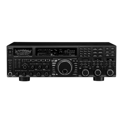
Yaesu Mark-V FT-1000MP Manual

©2002 VERTEX STANDARD CO., LTD. EH013H90A
Technical Supplement
HF Transceiver
This manual provides technical information necessary for servicing the Yaesu MARK-V
FT-1000MP
Field HF transceiver. It does
not include information on installation and operation, which are described in the MARK-V
FT-1000MP
Field Operating Manual, pro-
vided with each transceiver, or on MARK-V
FT-1000MP
Field accessories, which are described in manuals provided with each.
The MARK-V
FT-1000MP
Field is carefully designed to allow the knowledgeable operator to make nearly all adjustments required
for various station conditions, modes and operator preferences simply from the controls on the panels, without opening the case of the
transceiver. The MARK-V
FT-1000MP
Field Operating Manual describes these adjustments, plus certain internal settings.
Servicing this equipment requires expertise in handling surface mount chip components. Attempts by non-qualified persons to service
this equipment may result in permanent damage not covered by warranty. For the major circuit boards, each side of the board is identified
by the type of the majority of components installed on that side. In most cases one side has only chip components, and the other has either
a mixture of both chip and lead components (trimmers, coils, electrolytic capacitors, packaged ICs, etc.), or lead components only.
While we believe the technical information in this manual is correct, Vertex Standard assumes no liability for damage that may occur
as a result of typographical or other errors that may be present. Your cooperation in pointing out any inconsistencies in the technical
information would be appreciated. Vertex Standard reserves the right to make changes in this transceiver and the alignment procedures, in
the interest of technological improvement, without notification of the owners.
VERTEX STANDARD CO., LTD.
4-8-8 Nakameguro, Meguro-Ku, Tokyo 153-8644, Japan
VERTEX STANDARD
US Headquarters
17210 Edwards Rd., Cerritos, CA 90703, U.S.A.
International Division
8350 N.W. 52nd Terrace, Suite 201, Miami, FL 33166, U.S.A.
YAESU EUROPE B.V.
P.O. Box 75525, 1118 ZN Schiphol, The Netherlands
YAESU UK LTD.
Unit 12, Sun Valley Business Park, Winnall Close
Winchester, Hampshire, SO23 0LB, U.K.
VERTEX STANDARD HK LTD.
Unit 5, 20/F., Seaview Centre, 139-141 Hoi Bun Road,
Kwun Tong, Kowloon, Hong Kong

Contents
Specifications...................................................................................................................................................... 1-1
Exploded View & Miscellaneous Parts ............................................................................................................ 2-1
Alignment ........................................................................................................................................................... 3-1
Circuit Description ............................................................................................................................................ 4-1
Block & Interconnection Diagram................................................................................................................... 5-1
PCB Diagrams & Parts Lists
RF Unit ........................................................................................................................................................ 6A-1
IF Unit...........................................................................................................................................................6B-1
AF Unit .........................................................................................................................................................6C-1
INVERTER Unit.......................................................................................................................................... 6D-1
DDS-CAR Unit.............................................................................................................................................6E-1
I-DET Unit .................................................................................................................................................... 6F-1
LOCAL Unit ................................................................................................................................................ 6G-1
DDS-SUB Unit ............................................................................................................................................ 6H-1
DDS-PLL Unit ............................................................................................................................................... 6I-1
REF Unit ........................................................................................................................................................6J-1
CNTL-1 Unit................................................................................................................................................ 6K-1
DISPLAY Unit ..............................................................................................................................................6L-1
LPF-1 Unit ...................................................................................................................................................6M-1
PA Unit......................................................................................................................................................... 6N-1
TUNER-MAIN Unit .................................................................................................................................... 6O-1
TUNER-CNTL Unit ..................................................................................................................................... 6P-1
ALC Unit ..................................................................................................................................................... 6Q-1
DSP-A Unit ...................................................................................................................................................6R-1
DSP-D Unit................................................................................................................................................... 6S-1
RX-2 Unit ..................................................................................................................................................... 6T-1
RX2PLL-DDS Unit ..................................................................................................................................... 6U-1
RX2CAR-DDS Unit .....................................................................................................................................6V-1
ANT Unit .....................................................................................................................................................6W-1
REG Unit ..................................................................................................................................................... 6X-1
SW-A, B, C, D, E Unit..................................................................................................................................6Y-1
VR-A, B, C, D, E, F Unit..............................................................................................................................6Z-1
ENC-A, MIC, HP Unit...................................................................................................................................6a-1
KEY Unit ...................................................................................................................................................... 6b-1
LED Unit........................................................................................................................................................6c-1
PS Unit.......................................................................................................................................................... 6d-1
CAUTION
Danger of explosion if battery is incorrectry replaced.
Replace only with the same or equivalent type.

Specifications
1-1
General
Rx Frequency Range:100 kHz - 30 MHz
Tx Frequency Ranges:160 - 10m (Amateur bands only)
Frequency Stability:±0.5 ppm (after 1 min. @ 25 °C [77 °F])
±0.25 ppm (after 1 min. @ 25 °C[77 °F], w/TCXO-6)
Operating Temperature Range:–10 °C ~ +50 °C [+14 °F ~ +122 °F]
Emission Modes:LSB, USB, CW, FSK,AFSK,AM, FM
Frequency Steps:0.625/1.25/2.5/5/10 Hz for SSB,CW, RTTY & Packet;
100 Hz forAM and FM
Antenna Impedance:50 Ohms, unbalanced
16.6 - 150 Ohms, unbalanced (Tuner ON, TX only)
Power Consumption:AC 117V AC 200V DC 13.8 V
Rx (no signal) 70 VA 80 VA 2.3 A
Rx (signal) 80 VA 90 VA 2.7 A
100 W (CLASS AB) 450 VA 480 VA 20 A
25 W (CLASS A) 300 VA 320 VA 13 A
Supply Voltage:13.8 VDC/100-120 VAC 50-60 Hz/200-240 VAC 50-60 Hz
Dimensions (WHD): 410 x 135 x 347 mm ( 16 x 5.3 x 13.7 inch)
Weight (approx.): 15 kg. (33 lbs)
Transmitter
Power Output:Adjustable up to 100 watts (25 watts AM carrier),
Class A mode (SSB): 25 watts maximum
Duty Cycle:100% @ 50 watts, 50% @ 100 watts (FM & RTTY, 3-minute Tx)
Modulation Types:SSB: J3E Balanced, AM: A3E Low-level (early stage),
FM: F3E Variable reactance, AFSK: J1D, J2D Audio frequency shift keying
Maximum FM Deviation:± 2.5 kHz
FSK Shift Frequencies:170, 425, and 850 Hz
Packet Shift Frequencies:200 and 1000 Hz
Harmonic Radiation:Better than –60 dB (Typical)
SSB Carrier Suppression:At least 40 dB below peak output
Undesired Sideband Suppression:At least 55 dB below peak output
Audio Response (SSB): Not more than -6 dB from 400 to 2600 Hz
3rd-order IMD:–31 dB @ 100 watts PEP, or better
Class A mode: –40 dB @ 25 watts PEP (Typical)
Microphone Impedance:500 to 600 Ohms
Receiver
Circuit Type:Quad-conversion superheterodyne (triple conversion for FM)
Intermediate Frequencies:Main Rx; 70.455 MHz/8.215 MHz/455 kHz, Sub Rx; 47.21 MHz/455 kHz
Sensitivity:Modes 0.5 - 1.8 MHz 1.8 - 30 MHz
SSB/CW (2.0 kHz) 2 µV 0.16 µV
AM (6 kHz) 13 µV 2 µV
FM –0.5 µV
(with preamp on, IDBT on, SSB/CW/AM for 10 dB S/N, FM for 12 dB SINAD,
0 dBµ = 1 µV)
Selectivity (–6/–60 dB): Band Width Modes
Minimum –6 dB BW Maximum –60 dB BW
2.4 kHz all except FM 2.2 kHz 4.2 kHz
2.0 kHz all except FM 1.8 kHz 3.6 kHz
500 Hz
CW/RTTY/Packet
500 Hz 1.8 kHz
250 Hz
CW/RTTY/Packet
250 Hz 700 Hz
AM (Wide) 4 kHz 14 kHz
FM 8 kHz 19 kHz
IF Rejection (1.8 ~ 30 MHz): 80 dB or better (Main Rx), 60 dB or better (Sub Rx)
Image Rejection (1.8 ~ 30 MHz): 80 dB or better (Main), 50 dB or better (Sub)
Maximum Audio Output:2.0 W into 4 Ohms with <10% THD
Audio Output Impedance:4 to 8 Ohms
Specifications are subject to change, in the interest of technical improvement, without notice or obligation.

1-2
Notes

2-1
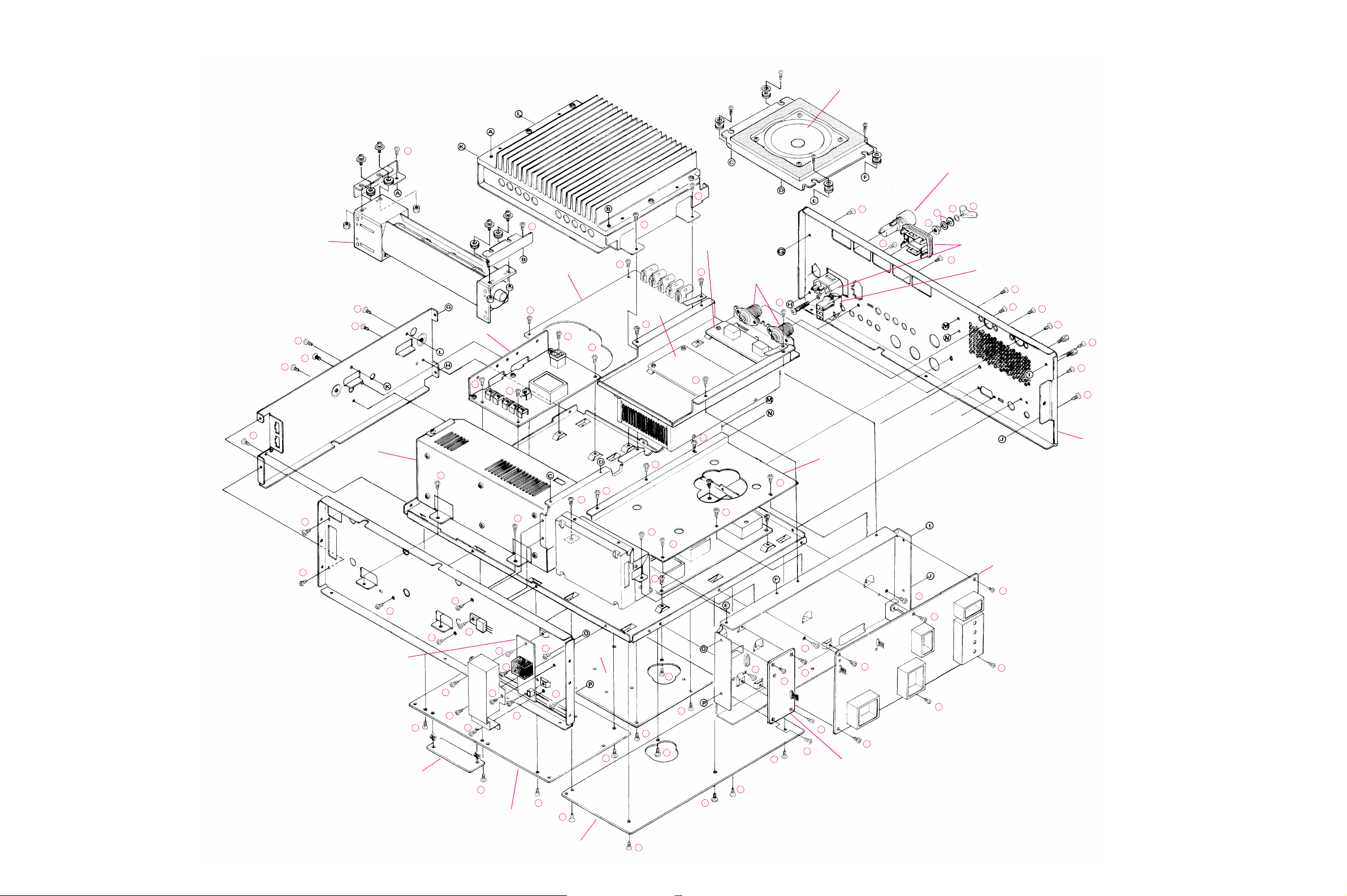
Exploded View & Miscellaneous Parts
RA0391000
CASE (BOTTOM)
S4000042
CASE LEG FT-015 (X2pcs)
R0133740
COIL SPRING (X2pcs)
R7133800
WASHER (X2pcs)
R3133080
COLLAR (X2pcs)
R3514230
LEG (X2pcs)
R3514220
LEG (X2pcs)
R0901050C
CASE (TOP)
R0151720
CASE (COVER)
R3151730
HOOK
R4115020
HANDLE HOLDER
R3084746
HANDLE
R0115070
HANDLE CORE
S4000025
FOOT FF-008 (X4pcs)
Ç
Ç
Ç
Ç
Ç
Ç
Ç
12
12
Ç
Ç
Ç
Ç
Ç
Ç
Ç
Ç
Ç
18
18
18
18
13
13
È
È
REF. VXSTD P/N Description Qty.
À
U00308001 PAN HEAD SCREW M3X8 1
Á
U00520002 PAN HEAD SCREW M5X20NI 1
Â
U03306001 SEMS SCREW ASM3X6 14
Ã
U04206001 SEMS SCREW HSM2.6X6 4
Ä
U20306001 BINDING HEAD M3X6 12
Å
U75703650
PLANE WASHER W3X8X0.5 FIBER
1
Æ
U20308001 BINDING HEAD M3X8 4
Ç
U20406007 BINDING HEAD M4X6B 16
È
U22416007 SEMS SCREW HM4X16B 2
É
U23306001 TAPTITE SCREW M3X6 4
11
U24305001 TAPTITE SCREW M3X5 41
12
U24306001 TAPTITE SCREW M3X6 137
13
U31415020
OVAL HEAD SCREW M4X15SUS
2
14
U24306007 TAPTITE SCREW M3X6B 14
15
U24308001 TAPTITE SCREW M3X8 10
16
U24310001 TAPTITE SCREW M3X10 6
17
U31306001 OVAL HEAD SCREW M3X6 6
18
U34306001 TAPTITE SCREW M3X6 5
19
U60300301 HEX NUT N3 1
20
U65500102 WING NUT N5NI 1
21
U65500002 FLANGE NUT N5NI 1
22
U70003001 PLANE WASHER FW3 4
23
U70005002 PLANE WASHER FW5NI 2
24
U73005002
TOOTHED LOCK WASHER IW5NI
2
25
U75703850
PLANE WASHER W3X8X1 FIBER
1
26
U9900062
TAPTITE SCREW M1.6X3NI#3
2
27
Q6000115 TERMINAL B-5 (M3) 2
28
S5000102 TAPTITE SCREW M2X4 4

2-2
Exploded View & Miscellaneous Parts
M4090125
SPEAKER
P2000067
FUSE HOLDER
P0090703
CONNECTOR
T9206441
WIRE ASS’Y
RA0387900
REAR FRAME
P1090352
CONNECTOR
(2pcs)
ANT Unit
ALC Unit
M2090011A
FAN
RF Unit
REG Unit
PS Unit
Q7000226
INV Unit
SSB-Filter Unit
IF Unit
CNTL Unit
AF Unit
REF Unit
RX2 Unit
Local Unit
18
12
12
12
12
12
12
12
12
12
12
12 12
12
12
12
12
12
12
12
12
12
12
12
12
12
12
12
12
12
12
12 12
12
12
12
12
12 12
12
12
12
12
12
12
12
12
12
12
12
12
12
12
12
12
12
12
12
12
12 12
12 12
12
12
12
12
12
16
16
Ã
Ã
Ã
Ã
Á
14
14
14
14
14 14
14
14
14
14
20
24
23
21
Æ
Æ
Æ
Æ
15
12

2-3
Exploded View & Miscellaneous Parts
RA0253800
KNOB
VR-E Unit
Q9000619
ROTARY ENCODER
LED Unit
R6151760
NUT
VR-C Unit
SW-C Unit
ENC-A Unit
VR-D Unit
SW-B Unit
Key Unit
Display Unit
HP Unit
SW-D Unit
MIC Unit
VR-B Unit
VR-B Unit
N4090148
PUSH SWITCH
SW-A Unit
VR-A Unit
R3151210A
KNOB
R3151220A
KNOB (X2pcs)
RA0388400
FRONT PANEL ASS’Y
R3521210A
KNOB (X2 pcs)
R3151500
KNOB (X2 pcs)
R3151490A
KNOB (X2 pcs)
R3152920A
KNOB
CP7273001
RING ASS’Y
R0136380
COIL SPRING
R0151140
SPRING
U9900059
POLY SLIDER
(X2 pcs)
R3521220A
KNOB MAIN ASS’Y
RA0256700
RUBBER RING
R3135000A
WASHER (X2 pcs)
R0134990A
COIL SPRING
R3521241
SUB MAIN ASS’Y
RA0256800
RUBBER RING
R0151190A
HOLDER
RA0257000
RUBBER TOP (X5 pcs)
RA02538A0
KNOB
RA02538B0
KNOB
RA02538A0
KNOB
RA0253800
KNOB
RA3151480A
KNOB (X5 pcs)
RA0390900
KNOB
15
15
15
15
12
12
12
12
12
12
12
12
12
12
12
12
12
12
12
12
12
12
26
26
11
11
11
11
12
11
11
11
11 11
11
11
11
11
11
11
11
11
11
11
11
11
11
11
11
11
11
12
12
12
12
12
12
É
É
É
É
Å
12 12
R6153330A
SPECIAL SCREW(X2 pcs)

2-4
Exploded View & Miscellaneous Parts
P1090352
CONNECTOR (2pcs)
HPF Unit
ANT Unit
ALC Unit
Tuner-Main Unit
Tuner-CNTL Unit
DSP-A Unit
DSP-D Unit
PA Unit
LPF Unit
11
11
11
11
16
16
16
16
16
16
11
11
12
12
12
12
12
12
12
14
14
14
14
Ä
Ä
Ä
Ä
Ä
Â
Â
Â
Â
Â
Â
Æ
ÆÆ
Æ
11
11
11
11
12
12
12
12
12
12
12
12
12
12
12
12
12
28
28
28
28

Alignment
3-1
Introduction and Precautions
The following procedures cover adjustments that are not nor-
mally required once the transceiver has left the factory. However,
if damage occurs and some parts subsequently be replaced, re-
alignment may be required. If a sudden problem occurs during
normal operation, it is likely due to component failure; realign-
ment should not be done until after the faulty component has been
replaced.
We recommend that servicing be performed by authorized Ver-
tex Standard service technicians, experienced with the circuitry
and fully equipped for repair and alignment. If a fault is suspected,
contact the selling dealer for instructions regarding repair.Autho-
rized Vertex Standard service technicians have the latest configu-
ration information, and realign all circuits and make complete per-
formance checks to ensure compliance with factory specifications
after repairs.
Those who do undertake any of the following alignments are
cautioned to proceed at their own risk. Problems caused by unau-
thorized attempts at realignment are not covered by the warranty
policy. Also, Vertex Standard must reserve the right to change cir-
cuits and alignment procedures in the interest of improved perfor-
mance, without notifying owners.
Under no circumstances should any alignment be attempted
unless the normal function and operation of the transceiver are
clearly understood, the cause of the malfunction has been clearly
pinpointed and any faulty components replaced, and the need for
realignment determined to be absolutely necessary.
The following test equipment (and thorough familiarity with
its correct use) is necessary for complete realignment. Most steps
do not require all of the equipment listed, but the interactions of
some adjustments may require that more complex adjustments be
performed in a sequence. Do not attempt to perform only a single
step unless it is clearly isolated electrically from all other steps.
Rather, have all test equipment ready before beginning, and fol-
low all of the steps in a section in the order they are presented.
Required Test Equipment
rDigital DC Voltmeter (high-Z, 1 MW/V)
rRF Millivoltmeter
rAC Voltmeter
rRF Standard Signal Generator w/calibrated output and dB scale,
0 dBµ = 0.5µV
rSignal Generator with calibrated output
rSpectrum Analyzer (60 MHz) or receiver (30 MHz)
rFrequency Counter
r50 WDummy Load (200 watts)
r16.6 WDummy load (200 watts)
rIn-Line Wattmeter (200 watts, 50 W)
rLinear Detector
rRF Coupler
Alignment Preparation & Precautions
A 50 Wdummy load and in-line wattmeter must be connected
to the antenna jack in all procedures that call for transmission,
expect where specified otherwise. Correct alignment is not pos-
sible with an antenna. Except where specified otherwise, the trans-
ceiver should be tuned to 14.2000 MHz, USB mode, and these
controls set as indicated:
¦MOX, VOX, AGC, PROC, IPO, ATT: OFF
¦MIC & RF PWR: fully CCW (minimum)
¦AF GAIN (Volume): As required
¦SQL: fully CCW (minimum)
¦NOTCH & SHIFT: to 12-o’clock
Read each step to determine if the same test equipment will be
required. If not, remove the test equipment (except dummy load
and wattmeter, if connected) before proceeding. Correct alignment
requires that the ambient temperature be the same as that of the
transceiver and test equipment, and that this temperature be held
constant between 20 ~ 30 °C (68 ~ 86 °F). If the transceiver is
brought into the shop from hot or cold air it should be allowed
time for thermal equalization with the environment before align-
ment. Alignments must only be made with oscillator shields and
circuit boards firmly affixed in place.Also, the test equipment must
be thoroughly warmed up before beginning.
Note: Signal levels in dB referred to in alignment are based on
0 dBµ = 0.5 µV.
Table Note: DC voltages should be within ±10 % of those listed
in the voltage tables.
REF Unit
Carrier Frequency
Refer to the drawing below for the REF Unit component loca-
tions and alignment points.
rConnect the frequency counter to pin 3 of J4703. Confirm the
frequency counter reading is 10.485760 MHz ±5 Hz.
TCXO Unit Test & Alignment Points
J4701 Pin-3
Carrier Frequency
Connect Frequency Counter (1.485760 MHz ± 5 Hz)
Alignment
3-2
RX2 Unit
Local Section 2nd OSC
Refer to the drawing at the page bottom for the RX2 Unit com-
ponent locations and alignment points.
rConnect the RF millivoltmeter to TP8004, then adjust T8016,
T8017, and T8018 in succession several times for peak RF
millivoltmeter indication.
2nd Local Frequency
rConnect the frequency counter to TP8004, then adjust T8018
for 46.755 MHz (± 600 Hz) on the frequency counter.
2nd Local Amplifier
rConnect the RF millivoltmeter to TP8004, then adjust T8016
and T8017 in succession several times for peak RF
millivoltmeter indication (at least 500 mVrms).
PLL BPF
rConnect the RF millivoltmeter to TP8003, then adjust T8012,
T8013, and T8014 in succession several times for peak RF
millivoltmeter indication (at least 60 mVrms).
PLL Loop VCO
rConnect the DC voltmeter to TP8005. Tune the transceiver
display to the frequencies shown in the chart below, and adjust
the components listed for the corresponding voltage, or else
confirm required voltages.
RX Section Interstage Transformers
rConnect the RF signal generator to the antenna jack.
rInject anRF signal (no modulation), and adjust T8002, T8004
~ T8007, T8009 ~ T8011, T8015, T8019, and T8020 in
succession several times for peak S-meter indication (adjust
the injection level as necessary to keep the meter around the
low side of the S-meter scale).
Tune to:
7.499 MHz
0.100 MHz
14.499 MHz
7.500 MHz
21.999 MHz
14.500 MHz
30.000 MHz
22.000 MHz
for
7.0 ± 0.1 V
1.3 ~ 2.5 V
7.5 ± 0.1 V
1.3 ~ 2.5 V
7.5 ± 0.1 V
1.3 ~ 2.5 V
7.0 ± 0.1 V
1.3 ~ 2.5 V
Adjust/Confirm
Adjust L8007
Confirm
Adjust L8010
Confirm
Adjust L8020
Confirm
Adjust L8024
Confirm
PLL Loop VCO Alignment
RX2 Unit Test & Alignment Points
VR8001
FM Squelch Threshold
T8020
RX2 RX IF Transformer
VR8007
S-Meter Full Scale
VR8006
IF Gain
T8019
RX2 RX IF Transformer
T8015
RX2 RX IF Transformer
T8007
RX2 RX IF Transformer
T8001
Noise Blanker
Connect DC Voltmeter
(minimum)
T8001
Noise Blanker
TP8004
2nd Oscillator: Connect RF Millivoltmeter (peak)
2nd Local Frequency: Connect Frequency Counter (46.775 MHz ± 600 Hz)
2nd Local Amplifier: Connect RF Millivoltmeter (>500 mVrms)
T8006
RX2 RX IF Transformer
L8007
PLL Loop VCO
L8010
PLL Loop VCO
L8020
PLL Loop VCO
L8024
PLL Loop VCO
TP8003
PLL BPF
Connect RF Millivoltmeter
(>60 mVrms)
T8012
PLL BPF
T8009
RX2 RX IF Transformer
T8010
RX2 RX IF Transformer
T8011
RX2 RX IF Transformer
T8002
RX2 RX IF Transformer
T8003
RX2 RX IF Transformer T8017
2nd Oscillator
2nd Local Amplifier
T8004
RX2 RX IF Transformer
T8005
RX2 RX IF Transformer
T8016
2nd Oscillator
2nd Local Amplifier
T8018
2nd Oscillator
2nd Local Amplifier
T8014
PLL BPF
T8013
PLL BPF
TP8005
PLL Loop VCO
Connect DC Voltmeter (7.0 V ± 0.1 V)

Alignment
3-3
IF Gain
rInject a +11 dBµ signal to the antenna jack, and tune the main
dial for peak indication on the S-meter.
rNow adjust VR8006 for 1-dot S-meter deflection.
S-Meter Full Scale
rInject a +100 dBµ signal to the antenna jack, and tune the main
dial for peak indication on the S-meter.
rAdjust VR8007 for S9 +60 dB on the S-meter.
FM Squelch Threshold
rIn FM mode, with no signal at the antenna jack, set the SQL
control to the 11-o’clock position.
rNow adjust VR8001 so that the squelch just closes.
SSB Squelch Threshold
rIn the SSB mode, with no signal at the antenna jack.
rConfirm that the SQL control is in the 9- to 12-o’clock posi-
tion whenthe squelch is just closed.
Noise Blanker
rConnect the DC voltmeter to TP8001, press the NB button,
then inject a +40 dBµ signal to the antenna jack.
rAdjust T8001 for minimum indication in the DC voltmeter.
Reduce the injection level to +23 dBµ and confirm that the
voltage is now less than 3.4 V.
Local Unit
Refer to the drawing at the page bottom for LOCAL Unit com-
ponent locations and alignment points.
2nd Local Oscillator
rConnect the RF millivoltmeter to TP4002, and adjust T4001
for maximum indication on the RF millivoltmeter (at least 400
mVrms), then turn T4001 1/4-clockwise futher more.
rReplace the RF millivoltmeter with a frequency counter at
TP4002, and confirm the frequency counter reading is 62.240
MHz (±600 Hz).
2nd Local Oscillator Amplifier
rRemove the coaxial plug from J4002, and connect a 50 W
resistor in parallel with the RF millivoltmeter across the socket.
rAdjust T4006 and T4007 in succession several times for peak
RF millivoltmeter indication (at least 170 mVrms).
rRemove the meter and resistor, and replace the plug into J4002.
WIDTH DDS Amplifier
rConnect the RF millivoltmeter to TP4004, and adjust T4010
for maximum indication on the RF millivoltmeter (at least 70
mVrms).
Local Unit Test & Alignment Points
TC4001
PLL Main Loop VCO
TC4002
PLL Main Loop VCO
TC4003
PLL Main Loop VCO
TC4001
PLL Main Loop VCO
T4009
3rd Local Amplifier
T4010
WIDTH DDS Amplifier
TP4004
WIDTH DDS Amplifier
Connect RF Millivoltmeter
(>70 mVrms)
T4006
2nd Local Amplifier
TP4002
2nd Oscillator:Connect RF Millivoltmeter (>400 mVrms)
Frequency Counter (62.24 MHz ± 200 Hz)
T4005
PLL BPF (67.98 MHz)

T4004
PLL BPF (67.98 MHz)
TP4001
PLL BPF (67.98 MHz): Connect RF Millivoltmeter (>100 mVrms)
T4002
PLL BPF (67.98 MHz)
J4002
2nd Local Amplifier:Connect 50 WDummy
in parallel with RF Millivoltmeter (>170 mVrms)
T4003
PLL BPF (67.98 MHz)
TP4003
PLL Main Loop VCO: Connect DC Voltmeter (8.5 V ± 0.1 V)
TP4005
PLL Main Loop VCO: Connect DC Voltmeter (1.65 V ± 0.01 V)
VR4001
PLL Main Loop VCO
J4003
3rd Local Amplifier: Connect 50 WDummy
in parallel with RF Millivoltmeter (>100 mVrms)
T4007
2nd Local Amplifier
T4008
2nd Local Amplifier

Alignment
3-4
3rd Local Amp
rRemove the coaxial plug from J4003 and connect a 50 Wre-
sistor in parallel with the RF millivoltmeter across the socket.
rAdjust T4008 and T4009 in succession several times for peak
RF millivoltmeter indication (at least 100 mVrms).
rReplace the RF millivoltmeter with a frequency counter at
J4003, and confirm that the frequency is 8.670 MHz (±30 Hz).
rRemove the frequency counter and resistor, and replace the
plug in J4003.
PLL BPF (67.98 MHz)
rConnect the RF millivoltmeter to TP4001, and adjust T4002
~ T4005 in succession several times for peak RF millivoltmeter
indication (at least 100 mV).
PLL Main Loop VCO
rConnect the DC voltmeter to TP4003.
rReferring to the table below, tune the transceiver to each fre-
quency, then confirm or adjust the listed component for the
required voltage.
rTune the transceiver display to 14.200 MHz. Connect the DC
voltmeter to TP4005, and adjust VR4001 for 1.65V (±0.05
V)on the DC voltmeter.
PA Unit
Refer to the drawing below for PA Unit component locations
and alignment points.
Idling Current (Class “AB”)
rTemporarily disconnect the jumper wire which connected be-
tween TP6101 and TP6102, and connect an ammeterin place
of the jumper.
rKey the transmitter in either USB or LSB with no microphone
input, and adjust VR6101 for 400 mA (±50 mA).
rReinstall the jumper.
Idling Current (Class “A”)
rTemporarily disconnect the jumper wire which connected be-
tween TP6101 and TP6102, and connect an ammeter in place
of the jumper.
rPress the CLASS-Aswitch. Key the transmitter in either USB
or LSB with no microphone input, and adjust VR9001 on the
REG Unit for 9.0 A (±0.2 A).
rDepress the CLASS-A switch, then reinstall the jumper.
Tune to:
7.499 MHz
4.000 MHz
3.999 MHz
0.100 MHz
14.499 MHz
7.500 MHz
21.999 MHz
14.500 MHz
30.000 MHz
22.000 MHz
for
8.5 ± 0.1 V
1.3 ~ 3.5 V
6.5 ~ 8.5 V
1.5 ~ 2.5 V
8.5 ± 0.1 V
1.3 ~ 2.3 V
8.5 ± 0.1 V
1.3 ~ 2.3 V
8.5 ± 0.1 V
1.3 ~ 2.3 V
Adjust/Confirm
Adjust TC4001
Confirm
Confirm
Confirm
Adjust TC4002
Confirm
Adjust TC4003
Confirm
Adjust TC4004
Confirm
PLL Main Loop VCO Alignment
PA Unit Test & Alignment Points
VR6101
Idling Current (Class-AB)
TP6101
Idling Current (Class-AB): Connect DC Ammeter
(400 mA ± 50 mA)
TP6102
Idling Current (Class-AB): Connect DC Ammeter
(400 mA ± 50 mA)

Alignment
3-5
LPF Unit
Refer to the drawing below for LPF Unit component locations
and alignment points.
CM Coupler Balance
rConnect the DC voltmeter to pin 3 of JP6002, connect a 50 W
dummy load to the antenna jack, and select the CW mode.
rKey the transmitter,and adjust TC6001 for minimum indica-
tion on the DC voltmeter.
TUNER-CNTL Unit
Refer to the drawing at the page bottom for TUNER-CNTL
Unit component locations and alignment points.
Tuning Capacitor/Motor
(Mechanical check, setting & adjustment)
rLoosen all set screws in the shaft coupler, and turn the coupler
by hand to confirm it moves freely (the motor and capacitor
should not move).
rIf the coupler binds, check the motor mounting position (it is
soldered in place) and the capacitor mounting screw.
rTurn the power switch off, and jumper TP6501 to chassis
ground. Turn the power switch on. The motor should rotate,
and then stop.
rSet the capacitor to its maximum capacitance position (plates
fully meshed) by hand, and tighten all shaft coupler set screw,
using care not to disturb the capacitor or motor positions.
rTurn the power off, and jumper TP6502 to chassis ground
(along with TP6501). Turn the power back on. The motor
should move 180°, and the capacitor should be then at mini-
mum capacitance (fully unmeshed). Remove the grounding
jumpers from TP6501 and TP6502.
Tuner Impedance & Phase Detection
rConnect the 50 Wdummy load and wattmeter to J6501 (the
output of the Tuner-Control Unit), and select the CW mode.
rConnect the DC voltmeter between pin-1 (IZIi) and pin-2 (IZIV)
of J6508 (either polarity).
rPress the TUNER and MOX buttons, adjust the RF PWRcon-
trol for 50 watts output, and then adjust TC6501, if necessary,
for meter indication within ±0.08 V of 0 V.
rWhile still transmitting, move the DC voltmeter to pin-3 (fC)
and pin-4 (fL) of J6508 (either polarity), and adjust VR6501,
if necessary, for meter indication within ±0.02 V of 0 V.
LPF Unit Test & Alignment Points
Tuner Unit Test & Alignment Points
TC6001
CM Coupler Balance JP6002
CM Coupler Balance: Connect DC Voltmeter (minimum)
TC6501
Tuning Impedance &
Phase Detection
J6501
Tuning Impedance &
Phase Detection:
Connect 50 WDummey with Wattmeter
J6508 Pin-4
Phase Detection:
Connect DC Voltmeter (0 V ± 0.02 V)
J6508 Pin-3
Phase Detection:
Connect DC Voltmeter (0 V ± 0.02 V)
J6508 Pin-1
Phase Detection:
Connect DC Voltmeter (0 V ± 0.08 V)
J6508 Pin-2
Phase Detection:
Connect DC Voltmeter (0 V ± 0.08 V)
VR6501
Phase Detection
TP6502
Tuning Capacitor:
Jumper to GND
TP6501
Tuning Capacitor:
Jumper to GND

Alignment
3-6
IF Unit
Refer to the drawing at the page bottom for IF Unit component
locations and alignment points.
2nd & 3rd Local Amplifiers
rConnect the RF millivoltmeter to TP2003, and adjust T2010
for maximum indication on the RF millivoltmeter (at least 450
mVrms).
rNext, connect the RF millivoltmeter to TP2005, and confirm
at least 100 mVrms.
Rx IF Interstage Transformer (I) (Coarse Alignment)
rConnect the RF signal generator to J2003, and inject a+100
dBu signal at 70.455 MHz. Connect the AC voltmeter across
and an 4 Wdummy load to the EXT SP jack on the rear panel.
rAdjust T2003 ~ T2009, T2011, and T2012 in succession sev-
eral times for peak indication on the AC voltmeter.
Receiver Section
RF Interstage Transformers (Coarse Alignment)
rPreset VR1001 and VR1002 to their 12-o’clock positions, and
select either USB or LSB mode. Adjust T1005 ~ T1009 on
the RF Unit in succession several times for peak noise from the
speaker.
S-Meter (Coarse Alignment)
rPreset VR2003 fully counter-clockwise, and adjust VR2003
so that all S-meter segments are just turned off. Preset the RF
GAIN control fully counter-clockwise, and adjust VR2002 for
S9+60 dB on the S-meter.
1st Mixer Balance
rTune the transceiver to 1.800 MHz, then adjust VR1001 and
VR1002 for minimum noise from the speaker.
IF Interstage Transformers (II)
rConnect the RF signal generator to the antenna jack, and inject
a +80 dBµ signal at 14.2000 MHz.
rSelect the USB mode,and tune the transceiver to 14.20220
MHz (so that a 2200 Hz tone is heard);adjust T1005 ~ T1009,
T2003 ~ T2009, T2011, and T2012 in succession several
times for peak S-meter indication (adjust the injection level as
necessary to keep the meter around mid scale).
IF Unit Test & Alignment Points
T2002
Noise Blanker
T2001
Noise Blanker
T2007
RX IF Transformer
T2006
RX IF Transformer
T2005
RX IF Transformer
T2015
TX IF Transformer
T2010
2nd & 3rd Local Amplifier
T2018
TX IF Transformer
TP2003
2nd & 3rd Local Amplifier:
Connect RF Millivoltmeter
(> 500 mVrms)
VR2006
TX 2nd Mixer
T2017
TX IF Transformer
VR2002
S-Meter Full Scale
VR2003
S-Meter
VR2008
CTCSS Tone Deviation
VR2009
FM Deviation
VR2007
COMP Meter Calibration
T2012
RX IF Transformer
T2011
RX IF Transformer
VR2005
IF Notch
L2004
IF Notch
T2009
RX IF Transformer
T2003
RX IF Transformer
T2019
TX IF Transformer
J2008
TX 2nd Mixer: Connect Spectrum Analyzer (minimize 2nd local spurious)
T2013
TX IF Transformer
T2008
RX IF Transformer
T2014
TX IF Transformer
T2004
RX IF Transformer TP2001
Noise Blanker:
Connect DC Voltmeter (minimum)
VR2001
FM Squelch Threshold L2026
FM Carrier Frequency

Alignment
3-7
RF Amplifiers
rConfirm that menu function 8-4 is set to “Tuned,” then connect
the RF signal generator to the antenna jack, and inject a +20
dBµ signal.
rReferring to the table below, tune the transceiver and RF signal
generator to the listed frequencies, and adjust the correspond-
ing components for the levels shown.
Tune SG & Radio to
1.910 MHz
3.725 MHz
7.110 MHz
28.200 MHz
for
Max S-meter
Max S-meter
Max S-meter
Max S-meter
Adjust
T1020
T1021
T1022
T1016
RF Amp Alignment
IF Gain
rTurn the transceiver off, then press and hold in the FAST and
LOCK buttons (near the main VFO knob), and turn the trans-
ceiver on again.
rConnect the RF signal generator to the antenna jack, and inject
a+11 dBµ signal. Select menu function 9-1, and adjust the
main VFO knob for a 1-segment S-meter deflection.
S-meter Full Scale
rConnect the RF signal generator to the antenna jack, and inject
a +100 dBµ signal.
rTune for peak indication on the S-meter. Now adjust VR2002
for S9+60 dB on the S-meter.
Noise Blanker
rSet menu function 2-8 to “A15,”then press the NB switch on,
and connect the DC voltmeter to TP2001.
rConnect the RF signal generator to the antenna jack and inject
a +40 dBµ signal, then adjust T2001 and T2002 in succession
several times for minimum DC voltmeter indication.
rReduce the RF signal level to +20 dBµ, and confirm at least
2.8 V on the DC voltmeter.
IF Notch
rPreset the NOTCH control to 12-o’clock, then inject a +30
dBµ signal at 14.2000 MHz to the antenna jack. Select USB,
then tune the transceiver to 14.20150 MHz (so that a 1500 Hz
tone is heard).
rPress the NOTCH button, then adjust VR2005 and L2004 for
minimum S-meter indication.
FM Squelch Threshold
rWith the FM mode selected, and no signal present, set the SQL
control to the 11-o’clock position, then adjust VR2001 so that
the squelch just closes.
RF Unit Test & Alignment Points
VRF
rTurn the transceiver off, then press and hold the [SUB]and
[ENT]keys of the keypad, and turn the transceiver on again.
rConnect the RF signal generator to the antenna jack, and inject
a +20 dBµ signal.
rPress the VRF button on the shuttle Jog, then adjust the VRF/
MEM CH knob to illuminate the “center” segment of the Ex-
panded Tuning Scale (above the main VFO-A frequency dis-
play).
rReferring to the table below, tune the transceiver and RF signal
generator to the listed frequencies, and adjust the correspond-
ing components for the levels shown.
Tune SG & Radio to
1.910 MHz
3.775 MHz
7.260 MHz
10.100 MHz
14.100 MHz
for
Max S-meter
Max S-meter
Max S-meter
Max S-meter
Max S-meter
Adjust
T1026 & T1027
T1028 & T1029
T1030 & T1031
T1032 & T1033
T1034 & T1035
VRF Alignment
T1022
Transmitter IF Interstage Transformer
T1020
Transmitter IF Interstage Transformer
T1016
Transmitter IF Interstage Transformer
VR1001
RF Interstage Transformers Coarse Alignment
1st Mixer Balance
VR1002
RF Interstage Transformers Coarse Alignment
1st Mixer Balance
T1009
IF Interstage Transformers (II)
T1008
IF Interstage Transformers (II)
T1007
IF Interstage Transformers (II)
T1005
IF Interstage Transformers (II)
T1006
IF Interstage Transformers (II)
T1021
Transmitter IF Interstage Transformer
T1034
VRF
T1032
VRF
T1030
VRF
T1028
VRF
T1026
VRF
T1035
VRF
T1033
VRF
T1031
VRF
T1029
VRF
T1027
VRF

Alignment
3-8
Transmitter Section
Tx 2nd Mixer
rSelect the CW mode, and connect the spectrum analyzer
(FCENTER = 70.455 MHz) to J2008.
rKey the transmitter, and adjust VR2006 to minimize the 2nd
local spurious (±8.2 MHz from the 2nd local frequency).
Transmitter IF Interstage Transformers
rConnect the 50 Wdummy load to the antenna jack. Preset the
RF PWR control fully clockwise, and MIC gain control fully
counter-clockwise. Select CW mode.
rKey the transmitter, and adjust T1001, T1002, T2013 ~
T2015, and T2017 ~ T2019 in succession several times for
maximum indication on the ALC meter.
Overcurrent ALC
rWith the inline wattmeter and 50 Wdummy load connected to
the antenna jack and the RF PWR control fully clockwise. Set
S3002 on theAF Unit to the “100W” position.
rTune the transceiver to 3.500 MHz, and select the CW mode.
Key the transmitter, and adjust VR3008 for 140 watts on the
wattmeter.
Maximum RF Power Output
rPreset the RF PWRcontrol fully clockwise, and tune the trans-
ceiver to 14.2000 MHz. Select the CW mode, key the trans-
mitter,and adjust VR3003 for 100 watts on the meter.
25 W and 10 W RF Power Output
rConnect the in-line wattmeter and 50 Wdummy load to the
antenna jack, select the CW mode,and tune to 14.2000 MHz.
rSet the menu function 4-0 to “Lo-2.”
Set the RF PWR control fully clockwise.
rKey the transmitter, and adjust VR3007 for 25 watts (±2 watts)
on the power meter.
rRecall menu function 4-0, and select “Lo-1.” Key the trans-
mitter, and adjust VR3006 for 10 watts (±1 watt) on the power
meter.
rAfter adjustment, recall menu function 4-0., then select “HI.”
TX Drive Control
rSet the RF PWR control fully counter-clockwise, and select
the CW mode. Key the transmitter, and adjust VR3013 so that
one segment is displayed on the PO meter.
ALC Meter Sensitivity
rSet the meter function toALC, then inject a 1 kHz tone at 4 mV
level to the microphone jack. Key the transmitter, and adjust
the MIC gain control so the meter just begins to deflect.
rIncrease the injection level to 10 mV, and adjust VR3005 so
that the meter deflects to the top edge of the ALC zone.
TX IF Gain
rTurn the transceiver off. Next, press and hold the FAST and
LOCK keys (near the main VFO knob), then turn the trans-
ceiver on.
rFor the frequencies listed in the table below, set the transceiver
to LSB mode, and inject a 1 kHz tone at 0.5 mV level to the
microphone jack. Set the MIC gain control fully clockwise. Be
sure to check the Menu display for the correct alignment item.
TX IF Gain Alignment
Menu
Function 9-2
T IF-018
T IF-035
T IF-070
T IF-100
T IF-140
T IF-180
T IF-210
T IF-245
T IF-280
T IF-290
Tune to:
1.800 MHz
3.750 MHz
7.150 MHz
10.125 MHz
14.175 MHz
18.100 MHz
21.200 MHz
24.900 MHz
28.500 MHz
29.500 MHz
Key Tx and adjust
Main VFO Dial for
MininumALC Indication
Note: For all adjustments below, set the transceiver to LSB,
and inject a 0.5 mV, 1-kHz to the MIC jack. Set the MIC
gain control fully clockwise.
TX IF Gain Alignment
AF Unit Test & Alignment Points
VR3014
PO Meter Calibration
VR3015
SWR Meter Calibration
VR3002
Overcurrent ALC
REV ALC
VR3005
ALC Meter Secsitivity
VR3012
SSB Modulation Balance
VR3013
TX Drive Control
VR3011
AM Carrier Level
VR3010
PKT RX AF Level Preset
VR3001
Key Beeper Level Preset
VR3009
SSB Squelch Threshold
VR3003
Maximum RF Power Output
VR3006
25 W and 10 W RF Power Output
VR3007
25 W and 10 W RF Power Output

Alignment
3-9
PO Meter Calibration
rWith the wattmeter and 50 Wdummy load connected to the
antenna jack, select the CW mode and set the meter to read
power output.
rKey the transmitter, and adjust the RF PWR control for 100
watts on the external wattmeter. Then adjust VR3014 so the
transceiver’s PO meter also indicates 100 watts.
Reverse ALC
rConnect the 16.6 Wdummy load (or three 50 Wloads in paral-
lel) to the antenna jack, preset theRF PWR control fully-clock-
wise,and select the CW mode. Key the transmitter, and adjust
VR3002 for 50 watts on the transceiver’s PO meter.
SWR Meter Calibration
rConnect the 16.6 Wdummy load (or three 50 Wloads in paral-
lel) to the antenna jack, then preset the RF PWR control fully
clockwise. Select the CW mode, and set the meter to read SWR.
rKey the transmitter, and adjust VR3015 so the meter indicates
3.0:1 SWR (within 1 bargraph segment).
IC Meter Calibration Check
rWith the wattmeter and 50 Wdummy load connected to the
antenna jack, select the CW mode, and set the meter to read
IC. Preset the RF PWR control fully clockwise.
rKey the transmitter, and confirm 12A ~ 21A IC meter indica-
tion.
SSB Modulator Balance
rWith the 50 dB attenuator and spectrum analyzer (or 50 W
dummy load and sampling coupler) connected to the antenna
jack, and the MIC gain control preset fully counterclockwise,
select either SSB mode. Alternatively, a separate receiver can
be used, with the transceiver connected to the dummy load.
rSet the menu function 8-9 to “-200.”
rKey the transmitter, and adjust VR3012 for minimum power
output (carrier leakage, which should be lower than -50 dB) as
indicated on the spectrum analyzer or external receiver.
AM Carrier Level
rWith the wattmeter and 50 Wdummy load connected to the
antenna jack, select the AM mode, and set the meter to read
ALC. With no microphone input, preset the RF PWR control
to the fully clockwise position. Key the transmitter, and adjust
VR3011 for ALC meter deflection to the top edge of theALC
zone.
COMP Meter Calibration
rSet the PROC and RF PWR controls fully clockwise, and
press the PROC button to activate the speech processor.
rSet the meter to read COMP, and preset the MIC gain control
to the 1-o’clock position. Inject a 1 kHz tone at 2 mV level to
the mic jack, and adjust VR2007 so that the transceiver’s
COMP meter deflects to the 10 dB mark on the COMP scale.
FM Carrier Frequency
rWith the 50 dB attenuator and frequency counter (or 50 W
dummy load and sampling coupler) connected to the antenna
jack, preset the FM mic gain control fully counter-clockwise,
select the FM mode, and tune to 29.0000 MHz. Key the trans-
mitter, and adjust L2026 for 29.0000 MHz (±50 Hz)on the
frequency counter.
FM & CTCSS Tone Deviation
rWith the 50 dB attenuator and linear detector (or 50 Wdummy
load and sampling coupler) connected to the antenna jack, se-
lect the FM mode, and tune to 29.2000 MHz.
rSet the FM mic gain control fully clockwise, and inject a 1 kHz
tone at 10 mV level to the mic jack. Key the transmitter, and
adjust VR2009 for ±2.3 kHz (±0.1 kHz)on the linear detector.
rSelect the 88.5 Hz (default) subaudible tone, and press the RPT
button to activate CTCSS operation. Key the transmitter and
with no microphone input, and adjust VR2008 for 0.5 kHz
±0.1 kHz on the liner detector.
FM Mic Gain
rWith the 50 dB attenuator and linear detector (or 50 Ωdummy
load and sampling coupler) connected to the antenna jack, tune
to 29.200 MHz, and select FM mode.
rInject a 1.8 mV signal at 1 kHz to the MIC jack. Key the trans-
mitter, and adjust VR6807 for 1.75 kHz ±0.1 kHz on the lin-
ear detector.
Transmitter Carrier Point
rTurn the transmitter off, then press and hold in the FAST and
LOCK buttons (near main VFO knob), then turn the transceiver
on.
rRecall menu function 9-0 and select “t-LsbcAr” using the
SUB VFO-B dial.
rSelect the LSB mode and then inject a 1 kHz tone to the mic
jack. Adjust the injection level to the point where theALC meter
no longer deflects.
rAdjust the injection frequency (within 800 ~ 2000 Hz) for peak
RF output, then adjust the injection level for 80 W RF output.
rSet the injection frequency to 350 Hz, and adjust the MAIN
VFO-A knob for 20 W RF output.
rSelect “t-uSbcAr” using the SUB VFO-B knob, and select the
USB mode. Inject a 1-kHz tone to the mic jack, and adjust the
injection level to the point where the ALC meter no longer
deflects.
rAdjust the injection frequency (from 800 ~ 2000 Hz) for peak
RF output, then adjust the injection level for 80 W RF output.
rSet the injection frequency to 350 Hz, and adjust the MAIN
VFO-A knob for 20 W RF output.

Alignment
3-10
Tuning Meter Center Preset
rSelect the CW mode, and turn the SPOT function on.
rConnect the DC voltmeter to the cathode of D6803, and adjust
the PITCH control for at least 4.0 V on the DC voltmeter.
rConnect the DC voltmeter to the “common” lead of VR6812,
and adjust VR6812 for 2.7 V (±0.1 V)on the DC voltmeter.
rConnect the DC voltmeter to pin 5 of J6802, and adjust
VR6802 for 3.4 V (±0.1 V)on the DC voltmeter.
rFinally, adjust VR6812 for a centered tuning meter indication.
Tuning Meter Preset (CW, RTTY and PKT Modes)
rRecall menu function 3-5, and select “A1-PitcH” using the
MAIN VFO-A knob. Tune to 700 Hz using the PITCH knob
(“C-700” displayed).
rSelect the CW mode, press the SPOT key, and adjust VR6811
for a centered tuning meter indication.
rSelect menu function 4-2, select the RTTY mode, and tune to
2210 Hz using the MAIN VFO-A knob.
rSelect “bEEP-tun” using the SUB VFO-B knob, and adjust
VR6810 for a centered tuning meter indication.
rTune a 2125 Hz beep frequency using the MAIN VFO-A knob,
and select the PKT mode.
rSelect “bEEP-tun” using the SUB VFO-B knob, and adjust
VR6809 for a centered tuning meter indication.
PKT Receiver AF Level Preset
rPreset VR3010 fully clockwise. The level should be adjusted
by the owner, if necessary.
Key Beeper Level Preset
rPreset VR3001 fully counter-clockwise. The “beep” level may
be reduced by the owner, if desired.
Headphone Output Level Preset
rPreset VR6804 ~ VR6807 to their 12-o’clock positions. The
level may be adjusted by the owner, if desired.
VOX Gain, ANTI TRIP and Delay Presets
rPreset VR6812 (DELAY), VR6813 (A-VOX) and VR6812
(VOX) to their 12-o’clock positions. These controls will be
adjusted by the owner during setup of the transceiver.
BEEP and SIDETONE Preset
rPreset VR5001 (SIDETONE) and VR5002 (BEEP) to their
10-o’clock positions. These controls may be adjusted by the
owner, if desired.
CNTL-1 Unit Test & Alignment Points
ALC Unit Test & Alignment Points
VR6811
Tuning Meter Preset
VR6810
Tuning Meter Preset
VR6809
Tuning Meter Preset
VR6806
VOX Gain, ANTI TRIP and Delay Presets
VR6805
VOX Gain, ANTI TRIP and Delay Presets
VR6808
VOX Gain, ANTI TRIP and Delay Presets
VR6807
VOX Gain, ANTI TRIP and Delay Presets
VR6804
Headphone Output Level Preset
VR6802
Headphone Output Level Preset
VR6803
Headphone Output Level Preset VR6801
Headphone Output Level Preset
VR6812
Tuning Meter Center Preset
Connect DC Voltmeter (2.7 V ± 0.1 V)
D6803 (Cathode)
Tuning Meter Center Preset
Connect DC Voltmeter (4.0 V)
J6802 Pin-5
Tuning Meter Center Preset
Connect DC Voltmeter (3.4 V ± 0.1 V)
VR5001
Side Tone Preset
VR5002
BEEP Preset

Circuit Description
4-1
Main Receive Signal Circuitry
High-Frequency Circuit
The receive signal enters from ANT connector A or B,selected
by relays RL6452/RL6453 on the TUNER-MAIN Unit, and it then
passes through t/r relay RL6451 and is fed to connector J1003 on
the RF Unit from connector J6454.
The receive signal then passes through the “RX Antenna” an-
tenna switching relay RL1003 and an attenuator (-6 dB, -12 dB; -
18 dB when combined) which consists of resistors R1051-R1054
and relays RL1003 and RL1004.
If the VRF feature is engaged (available on 160-20 meters),
the signal thenenters a narrow band-pass “preselector” filter which
consists of relays RL1006-RL1015, coils T1026-T1036, and ca-
pacitors C1253-C1264 and C1282-C1285. The preselector, which
provides high-Q filtering ahead of any active devices in the re-
ceivercircuitry, protects the components in the front end from strong
out-of-band energy.
The receive signal then enters a 5th-order Chebyshev low-pass
filter (LPF) which consists of coils L1087 and L1088 and capaci-
tors C1035-C1039.After the signal is removed of frequency com-
ponents of 30 MHz and above, it is fed to one of the band-pass
filter (BPF) networks.
The BPF is a 5th-order Chebyshev type filter; a total of 11
different bandpass filters are provided, covering the frequency range
100 kHz ~ 30 MHz in segments of different widths. Depending on
the receiver frequency, the appropriate band is selected by diodes
D1008-D1017(all 1SV271), D1018-D1026(all 1SS356),D1027-
D1031 (all 1SV271), and D1032-D1036 (all 1SS356).After re-
moval of unwanted frequency components, the incoming RF en-
ergy is applied to the high-frequency amplifier circuit.
The RF amplifier consists of alow-band amplifier circuit FET
Q1018 (3SK131), amid-band amplifier circuit FETsQ1019-
Q1022 (all SST310), and ahigh-band amplifier circuit Q1028
(SST310). The appropriate amplifier circuit is selected* by D1037-
D1041 and D1045 (all 1SS356).After amplification, the signal is
applied to the 1st mixer circuit and/or the sub-receive circuit (RX2
Unit).
* Note - If “Flat” is selected in Menu Program 8-4, RF signal
input is sent to the mid- band amplifier circuit.
Diodes D1046 andD1047 (both 1SS356), which are connected
to the RF amplifier input and output, turn on (off) the amplifier
circuit via the front-panel IPO switch.
1st Mixer Circuit/1st IF Circuit
The 1st mixer of the RF Unit consists of junction FETsQ1010-
Q1013 (allSST310). The 1st local signal (70.555 ~ 100.455 MHz)
from the LOCAL Unit is amplified by Q1014 (2SC2053)and
applied to the gates of each FET in the 1st mixer.
The resulting output signal (the difference between the local
signal and receive signal) passes through dual monolithic crystal
filters(MCF) XF1001/1002 (70R12BUF, BW: ±6 kHz) to obtain
the 1st IF signal having a center frequency of 70.455 MHz. The
signal is fed to the 2nd mixer circuit of the IF Unit after it is ampli-
fied by FET Q1009 (2SK131).
2nd Mixer Circuit/2nd IF Circuit
The 2nd mixer consists of FETsQ2020 and Q2024 (both
2SK302GR)onthe IF Unit. The 2nd local signal (62.24 MHz)
from the LOCAL Unit is amplified by Q2027 (2SC2812)and is
applied to each FET’s gate in the 2nd mixer.
The output from the 2nd mixer passes through monolithic crystal
filter XF2001, where it is stripped of unwanted signal components
to become the 2nd IF signal (8.215 MHz).A portion of the 2nd IF
signal from the mixer output is fed to the FM IF circuit through a
noise blanker circuit and buffer-amplifier FET Q2003
(2SK302GR).
The 2nd IF signal that has passed through the MCF enters the
noise blanker gate,D2014 (1SS226). It is then routed through
either a crystal filter (XF2002, XF2003, U2002, U2005) or an
attenuator (R2174, R2175, R2183), according to the receiving
mode (CW, SSB, or AM), and then it passes onward to the 3rd
mixer circuit.
Noise Blanker Circuit
A sample of the 2nd IF circuit is amplified by FETsQ2009 and
Q2010 (both 3SK131)on the IF Unit,and then undergoes detec-
tion by D2006 (1SS226). This output passes through R2017 and
R2027, C2006, and Q2001 (2SC2812)to yield an average AGC
voltage for controlling the degree of amplification of the above
FETs. Noise pulses contained in the output from D2026 are de-
tected by D2009 (1SS270)and Q2012 (2SC2812)and are used
to control the NB Gate.
3rd Mixer Circuit/3rd IF Circuit (IF Notch Circuit)
The 3rd mixer uses double-balanced mixer (DBM) IC Q2021
(µPC1037H)on the IF Unit. The 3rd local signal (8.67 MHz)
from the LOCAL Unit is applied to the DBM IC local port after it
is buffer-amplified by Q2028 (2SC2812). The signal output from
the 3rd mixer passes through a ceramic filter, crystal filter, or me-
chanical filter (U2001, U2003, U2004, U2006, CF2002), to be-
come the 455-kHz 3rd IF signal.
The 3rd IF signal,buffer-amplified by Q2022 (2SC2812),
passes through a notch frequency control circuit which consists of
L2004, C2063, C2064, and D2020 (HVU306A). Attenuation in
the IF notch circuit is controlled by VR2005. The3rd IF is then
buffer-amplified by Q2023 (2SC2812)and further amplified in
two stages by FETsQ2026 and Q2029 (both 3SK131).
The IF signal is then buffer-amplified by Q2004 and Q2017
(both 2SC2812), respectively. The output of Q2004 is applied to
theAF Unit through connector J2002, and the output from Q2017
is sent to theAGC circuit.
AGC Circuit
TheAGC circuit consists of D2012 and D2013 (both 1SS198),
transistor Q2018 (2SC2812), etc. on the IF Unit. Output from the

Circuit Description
4-2
AGC circuit is fed back to the RF AGC circuit that consists of
FETsand PIN diodes of the IF amplifier stages, by which the out-
put is controlled.
FM IF Circuit/FM Demodulator Circuit
The 2nd IF signal that has passed through buffer-amplifier FET
Q2003 on the IF Unit, and the 3rd local signal (8.67 MHz) that has
been buffer-amplified by Q2028,are fed to IC Q2015
(MC3372ML)for FM demodulation.
The FM demodulator IC contains a mixer, limiter amplifier,
filter amplifier, squelch trigger, and demodulator. The IF input sig-
nal is mixed with the 3rd local signal, band-limited by ceramic
filter CF2001 (CFWS455G,BW: ±4 kHz), amplified by the lim-
iter amplifier, and demodulated into an audio signal by the de-
modulator. It then passes through a filter (R2028, C2021) and con-
nector J2004 en route to the AF Unit. The signal then enters ana-
log switch IC Q3001-3 (BU4066BF)through a de-emphasis cir-
cuit which consists of R3060 and C3052.
The squelch circuit selectively amplifies the noise component
of the demodulator output by the filter amplifier inside the FM IC
and the active band-pass filter consisting of an externally attached
resistor and capacitor. This circuit uses a signal detected by D2001
(1SS270).
SSB/CW Demodulator Circuit
The 3rd IF signal from the IF Unit is applied to the SSB de-
modulator of Q3007 (µPC1037H)on the AF Unit, which pro-
duces audio by applying the carrier signal from the DDS-CAR
Unit to Q3007 after buffering by Q3020 (2SC2812). Similarly,
the CW signal is demodulated by a carrier signal which is offset by
the “Pitch”frequency.
The demodulated SSB and CW signals are each stripped of
high-frequency components by an active low-pass filter consisting
of op-amp IC Q3008-2 and IC Q3008-1 (M5218AFP). Then, they
enter analog switch IC Q3001-2 and IC Q3001-4 (BU4066BF).
AM Demodulator Circuit
The 3rd IF signal from the IF Unit is applied to I-DET Unit
U3003 on the AF Unit, from which it enters IC Q3703
(MC13020M)for AM demodulation.
The IC for AM demodulation consists mainly of an envelope
detector, VCO, phase shifter, synchronous detector, and DC/AC
detector. From the IF signal that is fed to the IC, the envelope
detector output and synchronous detector output are picked up.
The output from the demodulator circuit passes through ana-
log switches Q3701-1 and Q3701-2 for switching between the syn-
chronous detector output and envelope detector output. It then
enters analog switch IC Q3001-1 (BU4066BF)after removal of
the high-frequency components by an active low-pass filter which
consists of op-amp IC Q3013-1 (M5218AFP)on the AF Unit.
Low-Frequency Amplifier Circuit
The demodulated signal that is selected by one of analog
switches IC Q3001-1 to IC Q3001-4 on the AF Unit (according to
the receiving mode)passes through the squelch switch, audio mut-
ing FET Q3002 (2SK160), low-frequency amplifier transistor
Q3006 (2SC2812), electronic volume ICQ3005 (M51131L), op-
amp IC Q3014-1 (M5218AFP)for buffer-amplification, and IC
Q3022 (TDA2003V)for low-frequency power to drive the inter-
nal or external speaker with a maximum output of approximately
1.5 W. The signal that passes through electronic volume IC Q3005
is also sent to the headphone terminals after it is amplified by head-
phone amplifier IC Q3015-1 (M5218AFP).
Transmit Signal Circuitry
Microphone Amplifier Circuit
The audio signal from microphone jack J9421 on the MIC Unit
is passed through connector JP9421 and the DISPLAY Unit’s con-
nectors (J5528 and J5529), is amplified by transistor Q3048
(2SC2812)on the AF Unit, and then is applied to electronic vol-
ume IC Q3044 (M51131L),which is controlled by the MIC knob
on the panel.
The output (audio signal) from the electronic volume control
is amplified by Q3045 (2SC2812)and fed to balanced modulator
IC Q3046 (µPC1037H)through the buffer-amplifier transistor
Q3043 (2SC2812).
During FM transmission, the audio signal is routed to connec-
tor J2011 inside the IF Unit after its volume is adjusted by VR6814
on the ALC Unit. The audio signal that has passed through the pre-
emphasis circuit consisting of C2201 and R2228 on the IF Unit is
mixed with a tone signal from the CNTL Unit,and is amplified
and limited by op-amp IC Q2049-2 (M5223AFP)of the IDC cir-
cuit. The audio then passes through the splatter filter (secondary
active low-pass filter) formed by op-amp IC Q2049-1, R2229, and
R2230, plus C2119 and C2206, and is then fed to the frequency-
modulator circuit inside the IF Unit through VR2008 and VR2009
for setting of the frequency deviation.
SSB Modulator Circuit
The carrier signal appropriate to the transmitting mode (LSB
or USB) is applied from the CAR-DDS Unit to balanced modula-
tor IC Q3046 onthe AF Unit, and is modulated by microphone
audio.
The balanced modulator produces the upper and lower side
bands and carrier signal. The carrier and audio signal are suppressed
and the carrier balance is adjusted by VR3012. As a result, the
output signal obtained is a DSB signal with a carrier suppression
ratio of 35 dB or more.
The DSB modulated signal (1st IF signal: 455 kHz) then passes
through mechanical filter XF9801 inside the SSB-FIL Unit on the
IF Unit, stripping residual carrier and the undesired sideband; the
signal then passes as an SSB signal through buffer-amplifier Q3049
(2SC2812), connector J3026, and the IF Unit’s connector J2009.
Other manuals for Mark-V FT-1000MP
9
Table of contents
Other Yaesu Transceiver manuals

Yaesu
Yaesu FT-101ZD User manual

Yaesu
Yaesu FT DX 1200 User manual

Yaesu
Yaesu FTDX101MP User manual

Yaesu
Yaesu FT DX 3000 User manual

Yaesu
Yaesu FT-902DM User manual

Yaesu
Yaesu FTC-703A User manual

Yaesu
Yaesu FT-2800M User manual

Yaesu
Yaesu FTdx3000 Series Manual

Yaesu
Yaesu VX-8R User manual

Yaesu
Yaesu FTDX-9000MP User manual

Yaesu
Yaesu FT-8100R Manual

Yaesu
Yaesu FT-897 User manual

Yaesu
Yaesu Mark-V FT-1000MP User manual

Yaesu
Yaesu DMU-2000 User manual

Yaesu
Yaesu FT-847 Manual

Yaesu
Yaesu FTM-500DR User manual

Yaesu
Yaesu FTM-400DR User manual

Yaesu
Yaesu FT-2400H User manual

Yaesu
Yaesu VX-2R User manual

Yaesu
Yaesu VX-8DR User manual