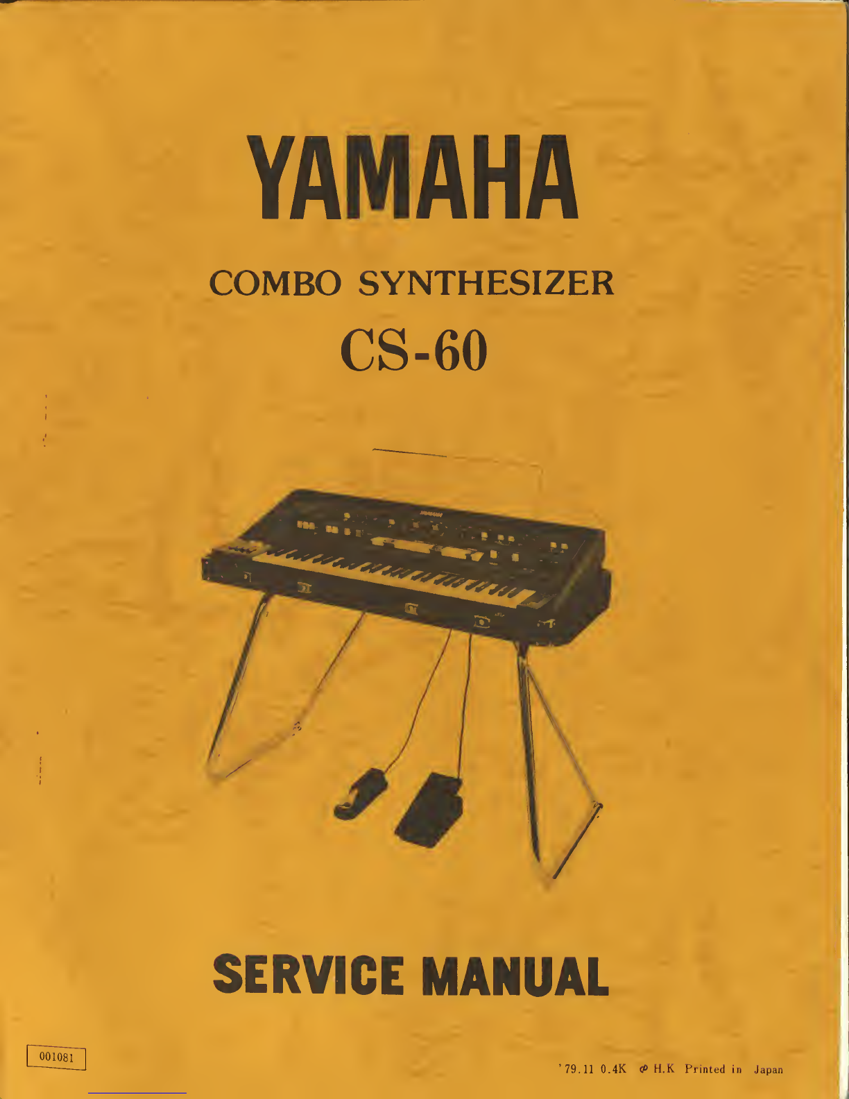
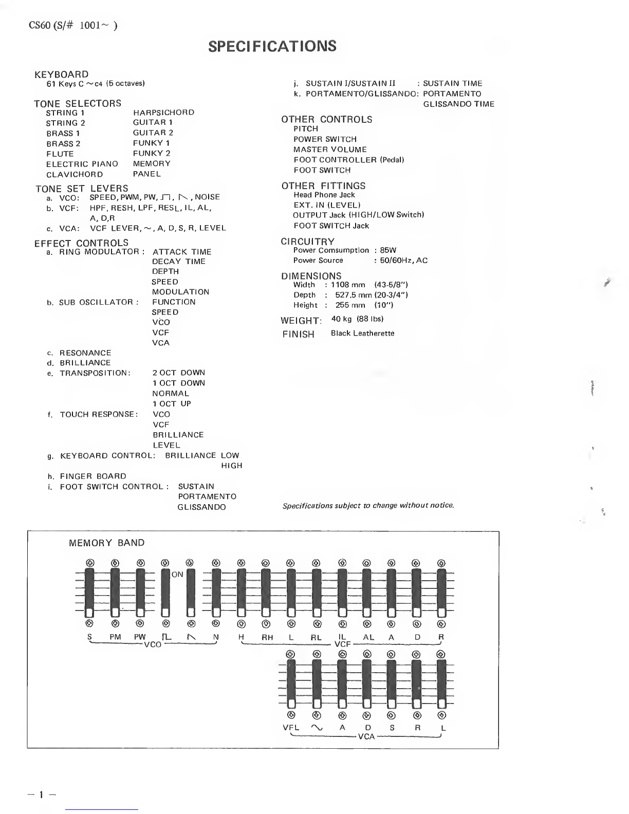
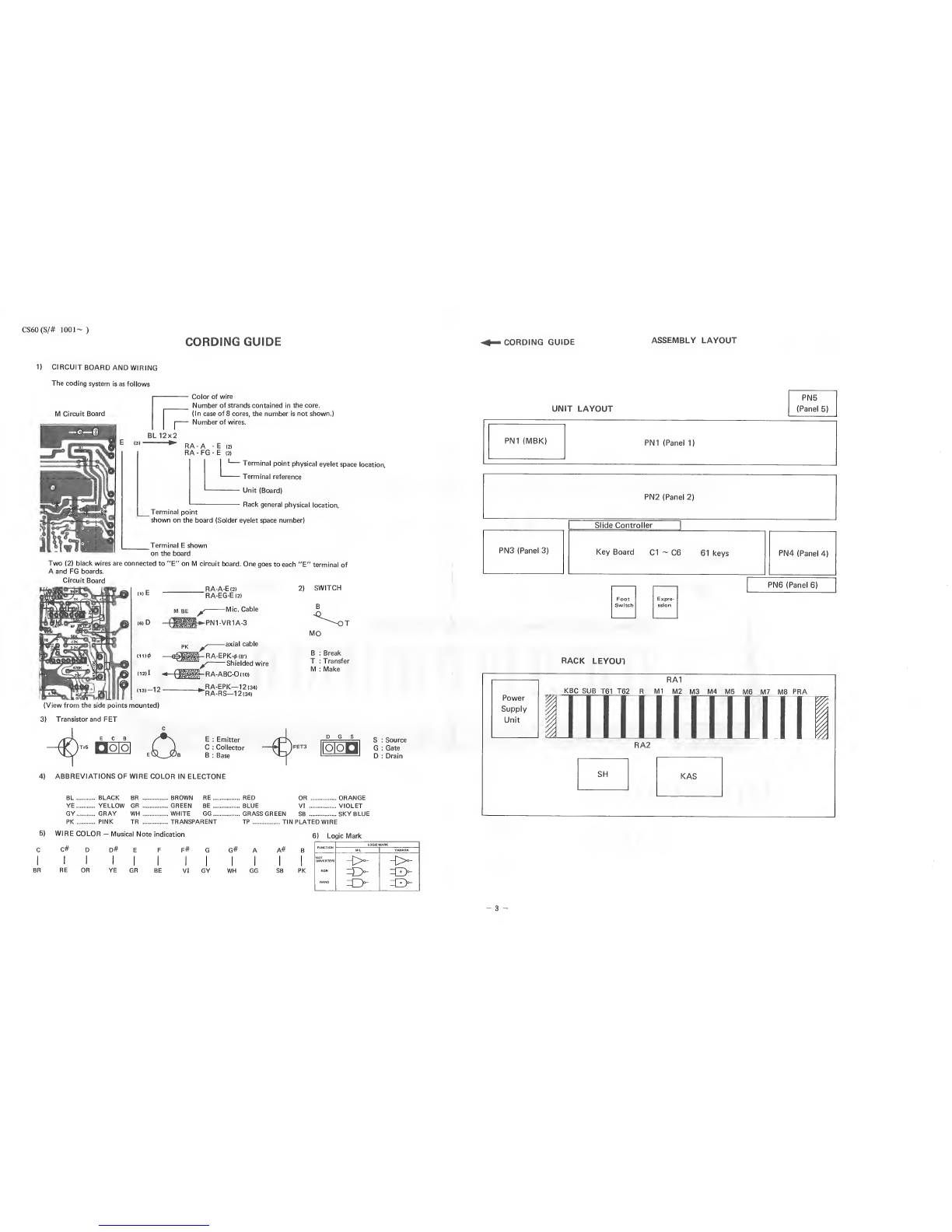
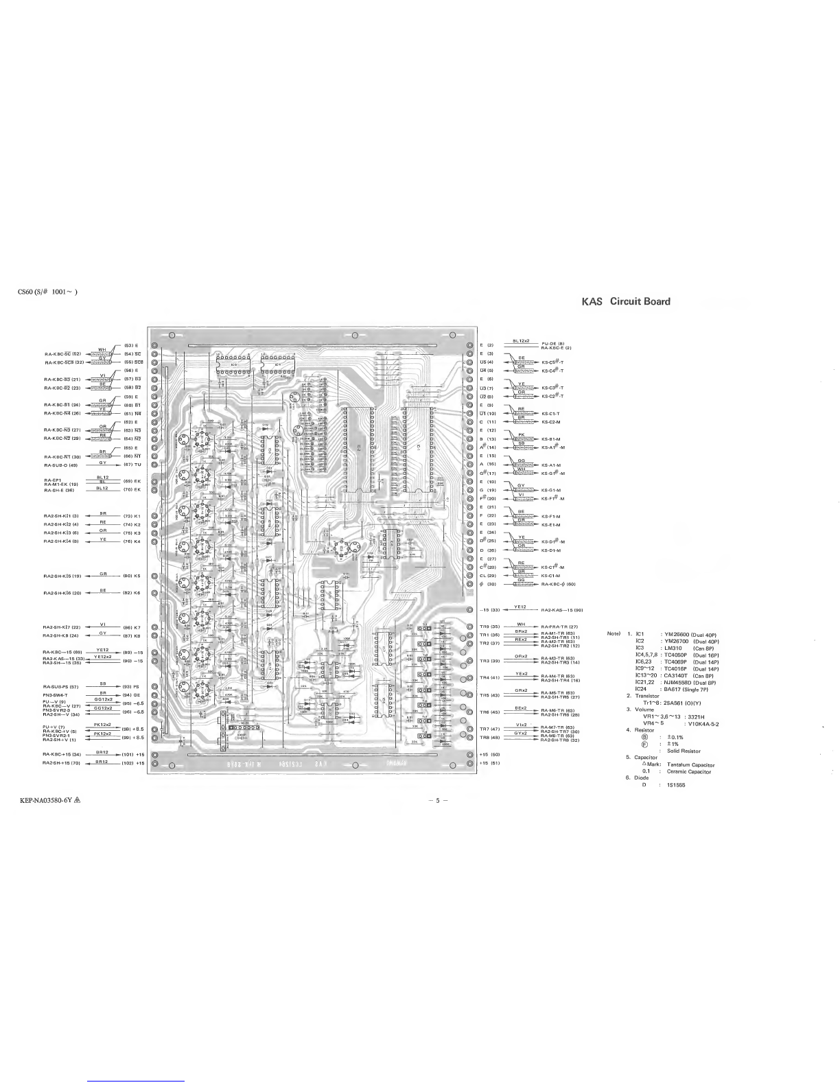
Yamaha CS-60 User manual

YAMAHA
COMBO SYNTHESIZER
CS-60
SERVICE MANUAL
79.11 0.4K <P H.K Printed in Japan

CS60(S/# 1001- )
INDEX
\
CS-60 SPECIFICATIONS 1
CS-60 PANEL LAYOUT 2
CS-60 CORDING GUIDE ASSEMBLY LAYOUT (UNIT &RACK) 3
KAS (Key Assigner) Circuit 4
SH (Sample Hold) Circuit 7
KBC Circuit 9
SUB (Sub Oscillator) Circuit 11
PRA (Pre-Amp) Circuit 13
M(Master) Circuit 15
R6 (Registor) Circuit 23
T61 (Tone Preset 1)Circuit 25
T62 (Tone Preset 2) Circuit 27
SVU Circuit 29
Power Supply NP0013Z (Primary) Circuit 30
PN i(Panel 1)Circuit 31
PN2 (Panel 2) Circuit 32
KS (Key Switch) Circuit 33
PN3,PNs, PNe, PU, EXP &FOOT SW Circuit 34
CIRCUIT ADJUSTMENT
CS-60 Parts List

CS60(S/# 1001- )
SPECIFICATIONS
KEYBOARD
61 Keys C~c4 (5 octaves)
TONE SELECTORS
STRING 1
STRING 2
BRASS 1
BRASS 2
FLUTE
ELECTRIC PIANO
CLAVICHORD
HARPSICHORD
GUITAR 1
GUITAR 2
FUNKY 1
FUNKY 2
MEMORY
PANEL
TONE SET LEVERS
a. VCO: SPEED, PWM,PW,n, |\ ,NOISE
b. VCF: HPF, RESH, LPF, RESL, IL, AL,
A, D,R
c. VCA: VCF LEVER, ~, A, D, S, R, LEVEL
EFFECT CONTROLS
a. RING MODULATOR :ATTACK TIME
DECAY TIME
DEPTH
SPEED
MODULATION
FUNCTION
SPEED
VCO
VCF
VCA
b. SUB OSCILLATOR
RESONANCE
BRILLIANCE
TRANSPOSITION: 2OCT DOWN
1OCT DOWN
NORMAL
1OCT UP
f. TOUCH RESPONSE: VCO
VCF
BRILLIANCE
LEVEL
g. KEYBOARD CONTROL: BRILLIANCE LOW
HIGH
FINGER BOARD
FOOT SWITCH CONTROL SUSTAIN
PORTAMENTO
GLISSANDO
j. SUSTAIN I/SUSTAIN II :
k. PORTAMENTO/GLISSANDO: SUSTAIN TIME
PORTAMENTO
GLISSANDO TIME
OTHER CONTROLS
PITCH
POWER SWITCH
MASTER VOLUME
FOOT CONTROLLER (Pedal)
FOOT SWITCH
OTHER FITTINGS
Head Phone Jack
EXT. IN (LEVEL)
OUTPUT Jack (HIGH/LOW Switch)
FOOT SWITCH Jack
CIRCUITRY
Power Comsumption
Power Source
85W
50/60Hz, AC
DIMENSIONS
Width
Depth
Height
WEIGHT:
FINISH
1108 mm (43-5/8")
527.5 mm (20-3/4")
255 mm (10")
40 kg (88 lbs)
Black Leatherette
Specifications subject to change without notice.
MEMORY BAND
®®
pm pw n_
VCO —(X
s> ®©©®© © ©©
1RH LRL IL AL
©
A
©
D
©
n
©©©©
©®©®©©©
VFL
v. 'V AD
-VCA- SRL
j

Panel Layout
CS60(S/# 1001- )
_G BIBS MOBUUTDB 1„'rr, SUB BStlliim ,tsmun Hallux
mm BEtAT DEPTH SPEED HOOUUIIC* FIICTIM SPEED VCO »EF VGA BESMMCE BS1LUMCF
fWrV.il9W 9
TFUISFDEnill —
.
T^™ffiiia ""SSSST1"""
9Tf9
VFL -V ADSRL
1VCA '
2-

CS60(S/# 1001- )CORDING GUIDE CORDING GUIDE ASSEMBLY LAYOUT
1) CIRCUIT BOARD AND WIRING
The coding system is as follows
MCircuit Board
Color of wire
Number of strands contained in the core.
(In case of 8cores, the number is not shown.)
Number of wires.
E(3)' BL12x2 RA -A-E(2)
RA -FG -E(2)
_Terminal point
shown on the board (Solder eyelet space number)
Terminal Eshown
on the board
Terminal point physical eyelet space location.
Terminal reference
Unit (Board)
Rack general physical location.
Two (2) black wires are connected to "E" on IV! circuit board. One goes to each "E" terminal of
Aand FG boards.
Circuit Board
d)E
(6)D
(11)0
(12)1
(13J-12
(View from the side points mounted)
3) Transistor and FET
RA-A-E(2)
RA-EG-E(2)
MBE A-Mic Cable
2) SWITCH
B
|§*-PN1-VR1A-3
PK jT -axial cable
|-RA-EPK-0(ff)
Shielded wire
jr
Hj-RA-ABC-Odo)
MO
B:Break
T:Transfer
M:Make
RA-EPK—12(34)
RA-RS—12(34)
ECB
Tr5 oo E:Emitter
C:Collector
B:Base -€> D G S
FET3 OO S:Source
G:Gate
D:Drain
4) ABBREVIATIONS OF WIRE COLOR IN ELECTONE
BL BLACK BR BROWN RE RED OR ORANGE
YE YELLOW GR GREEN BE BLUE VI VIOLET
GY GRAY WH WHITE GG GRASS GREEN SB SKY BLUE
PK PINK TR TRANSPARENT TP TIN PLATED WIRE
5) WIRE CO LO R-Musical Note indication
CC# DD# EFF#
6) Logic Mark
BR
I
RE OR YE GR BE VI GY
G#
WH GG
A# B
SB PK
FUNCTION LOGIC MARK
MIL YAMAHA
NOT
(INVERTER)
NOR
NAND
->-
UNIT LAYOUT PN5
(Panel 5)
PN1 (MBK) PN1 (Panel 1)
PN3 (Panel 3)
Power
Supply
Unit
Key Board C1 ~C6 61 keys PN4 (Panel 4)
Foot
Switch Expre-
ssion
PN6 (Panel 6)
RACK LEYOU1
RA1
KBC SUB T61 T62 RM1 M2 M3 M4 M5 M6 M7 M8 PRA
!I I 1
RA2
SH KAS

KAS (Key Assigner) Circuit
CS60(S/# 1001- )
Note) 1. IC1 YM26600 (Dual 40P)
IC2 YM26700(Dual40P)
IC3 LM310 (Can8P)
IC4,5,7,8 TC4050P (Dual 16P)
IC6,23 TC4069P (Dual 14P)
IC9~12 TC4016P (Dual 14P)
IC13~20 CA3140T(Can8P)
IC21.22 NJM4558D (Dual 8P)
IC24 BA617 (Single 7P)
2. Transistor
Tr1~8 2SA561 (0)(Y)
3. Volume
VR1~3,(5~13 :3321H
VR4,5 :V10K4A-5-2
4. Resistor
(D Mark :±0.1%
©Mark :+1%
•X Mark :Solid Resistor
5. Cananitnr
0.1 :Ceramic Capacitor
AMark Tantalum Capacitor
6. Diode
D:1S1555
7. Power Suppl
Dual 14Pysill
1«*» §££ 00
/-6.5 ^-1
Dual 16P 1+8.5
8-6.5
Connect 3, 5, 7pins of IC5 to —6.5
Connect 7, 9pins of IC7 to -6.5
Connect 7, 9pins of IC8
Connect arrow-marks in this circuit as below
AMark to +15
AMark to -15
I50H51)
0+15(101)1102)
O-15(891(90)
OEK (691(70)
KEC-4455-69A

CS60(S/# 1001- )KAS Circuit Board
RA-KBC-SC (52)
RA-KBC-SC8 (32) -
RA-KBC-B3 (21)
RA-KBC-B2 (23)
RA-KBC-B1 (24)
RA-KBC-N4 (26)
RA-KBC-N3 (27)
RA-KBC-N2 (29)
RA-KBC-N1 (30)
RA-SUB-O (49)
RA-EP1
RA-M1-EK (19)
RA-SH-E (36)
RA2-SH-KI1 (3) -*-
RA2-SH-KI2 (4) —-
RA2-SH-KI3 (6) -»-
RA2-SH-KI4 (8) -»-
RA2-SH-KIS (19) -*-
RA2-SH-KI6 (20)
RA2-SH-KI7 (22) -*-
RA2-SH-K8 (24) -*-
RA-KBC—15 (69)
RA2-KAS—15 (33)-»-
RA2-SH—15 (35) -*-
RA-SUB-PS (57)
PN3-SW4-T
PU—V(9)
RA-KBC—V(27)
PN3-SVR2-3
RA2-SH—V(34)
PU-+V (7)
RA-KBC-+V (5)
PN3-SVR2-1
RA2-SH-+V (1)
RA-KBC-+15 (34)
RA2-SH-+15 (70)
YE
^^
(53) E
(54) SC
(55) SCS
(56) E
(57) B3~
(58) H2
(59) E
(60) B1
(61) N4
(62) E
(63) N3
(64) N2
(65) E
(66) NT
(67) TU
(69) EK
(70) EK
(73) K1
(74) K2
(75) K3
(76) K4
(80) K5
(82) K6
(86) K7
(87) K8
-— (89)
(90)
-16
-15
(93) PS
-»- (94) GE
(95) -6.5
(96) -6.5
;(98) +8.5
;(99) +8.5
(101) +15
.(102) +15
ooo
o
SO J
JJIIIIIIlll o
22 Kc•III n
22K c)
o
o's o
<)
22K
22K o)
22K 3
22K SO o
1^v. fl >
22K o o
22K
22K o^t* i
n•^ v-'i]o
22 Kuo
J
-o r~*> o
22 K
22K
1.
r
100F
<XS\JD--
«>C oJ-
)
3
3
c
.
::•
soLrx. 3
=li
8I*
J"
J
1C-24 7
Upo OP]
<
3)
1000P
—Ih-
CD
^
i
»< J«
o
o3
'i
3
3
J
mm S~\-l 0-
hi- io on
loon
-ii- io on
io on
hh loon
33 K
ip on
0.01 Tr?
hi- loon
io on
©
o
0°
o®
o@
°®
o
o@
Ooo
E(2)
e: (3)
D5 (4)
03 (5)
E(6)
03 (7)
02 (8)
E(9)
UT (10)
C(11)
E(12)
B(13)
A# (14)
E(15)
A(16)
G#(17)
E(18)
G(19)
F# (20)
E(21)
F(22)
E(23)
E(24)
D# (25)
D(26)
E(27)
C#(28)
CL (29)
(30)
-15 (33)
TR9 (35)
TR1 (36)
TR2 (37)
TR3 (39)
TR4 (41)
TR5 (43)
TR6 (45)
TR7 (47)
TR8 (48)
+15 (50)
+15 (51)
^
-m
PU-DE (8)
RA-KBC-E (2)
BE KS-C5#-T
KS-C4#-T
KS-C3#-T
KS-C2#-T
£»" KS-C2-M
WH
VI
)•,
'.: ='
.BR
KS-B1-M
KS-A1*-M
KS-A1-M
KS-G1#-M
KS-G1-M
KS-F1#-M
KS-F1-M
KS-E1-M
KS-D1#-M
KS-D1-M
KS-Cfff-M
KS-C1-M
RA-KBC-0 (60)
RA2-KAS—15 (90)
-»- RA-PRA-TR (27)
-m- RA-M1-TR (63)
-"- RA2-SH-TR1 (11)
-»- RA-M2-TR (63)
-"- RA2-SH-TR2 (12)
RA-M3-TR (63)
RA2-SH-TR3 (14)
-»- RA-M4-TR (63)
-•* RA2-SH-TR4 (16)
-»- RA-M5-TR (63)
-*" RA2-SH-TR5 (27)
-»- RA-M6-TR (63)
"*" RA2-SH-TR6 (28)
-»- RA-M7-TR (63)
"*" RA2-SH-TR7 (30)
-»- RA-M8-TR (63)
-*" RA2-SH-TR8 (32)
Note) IIC1 :YM 26600 (Dual 40P)
IC2 :YM26700 (Dual 40P)
IC3 :LM310 (Can8P)
IC4,5,7,8 :TC4050P (Dual 16P)
IC6,23 TC4069P (Dual 14P)
IC9~12 TC4016P (Dual 14P)
IC13~20 CA3140T (Can8P)
IC21,22 NJM4558D (Dual 8P)
IC24 BA617 (Single 7P)
'?.. Transistor
Tr1~8 2SA561 (OXY)
3. Volume
VR1~ 3,6~13 :3321H
VR4~ 5:V10K4A-5-2
4. Resistor
®±0.1%
©±1%
Solid Resistor
5. Capacitor
AMark Tantalum Capacitor
0.1 Ceramic Capacitor
6. Diode
D1S1555
KEP-NA03580-6Y A5

CS60(S/# 1001- )
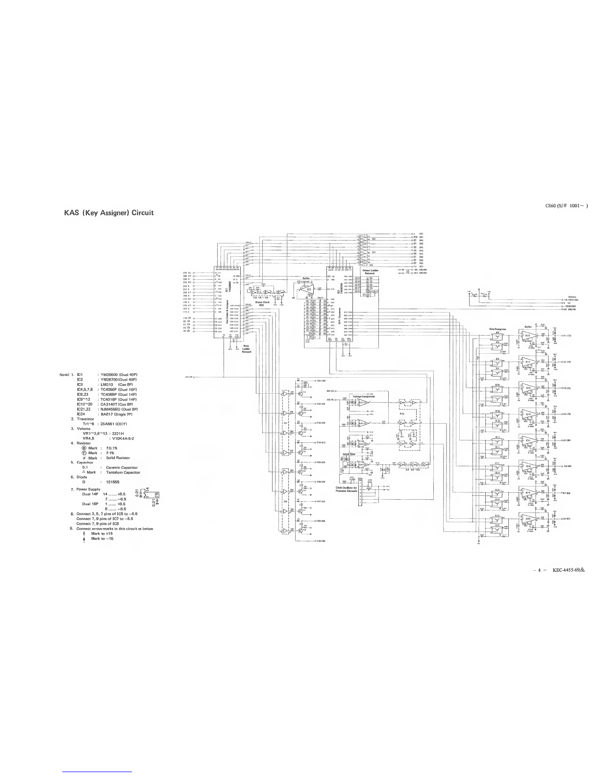
KEY CODER &KEY ASSIGNER LSI (YM26600) DA CONVERTER LSI (YM26700)
The LSI detects what keys are held down by judging the
pulse combination of the octave and note.
It also generates the seven bit key code, which is processed
by time sharing, in accordance with the key held down.
Pin. Pin
No. Name
VSS +8. 5V Power Supply
(p Master Clock Input
SC~ Synchro-clock Output
SC8 Synchro-clock Output on the first channel.
1.
2.
3.
4.
*jirinnjuuiJ¥uuuiiin-Mis KHZ
_1 29(1)
scfl TL_ _TL1/^
1Apulse is generated on the timing ofS
SCSflthe first channel. .,„ _
—'
''0-1 /8 SC
IC Initial Clear Input
Power SW ON
1
o[<-2±1 sec |J
On this timing, C4TTcode is memoried.
6. VDD —6.5V Power Supply Input
7.
8.
19.
20.
24.
25.
C#l Note on data input
When the key is depressed, the pulse is
supplied the corresponding pin of the note.
|*-H0.2mS
_TlMJl-JUn8'
-6.5
nKEY-ON
Octave on data input OFF
V5'
N1
When the key is depressed, the pulse is
supplied to the corresponding pin of the octave.
JlfUUl-JUE+8.5
-6.5
28. N4
KEY-ON
Note code data output
OFF
1:-6.5V 0: +8.5
V
C# DD# EFF# GG# AA# BC
N1 11111111
N2 1111111 1
N3 111111
N4 111111
29.
31.
B1
B3
Octave Code Data Output
1: -6.5V 0:+8.5V
C2 C2#-'C3 C3#~C4 C4#~C5 C5#~C6
B1 11
B2 111
B3 1 1 1
32.
39.
K01-1
)L.„. Key on
K08/ Data Output
OFF
KEY-ON
+8.5 (0)
-6.5V (1)
The time shared key data is supplied to the LSI. Analog
DC voltage is produced in corporation with key by the data
and supplied to each channel.
VSS +8. 5V Power Supply
SC8 Synchro-clock input on the first channel.
POR Portamento and Glissando operation. When
the portament VR is turned on, +8.5V is
supplied to the pin and actuate.
PC Clock input for Portament and Glissando
operation.
U1 .4sec.~1 .4msec.»|
_r
—
ljr
—J ''L— -6.5V
The frequency is variable by Changing the
portamento VR.
N1
11. B3
Note code data input
Note code data is supplied to the pins from
key coder LSI.
.Octave code data input
Octave code data is supplied to the pins
from key coder LSI.
12. OO Output for octave key voltage. (8ch time
sharing)
Provided the output key voltage for the
octave selected from octave code.
13. OCT0\ Input for octave key voltage.
18. OCT5'
*TU pin: 4.0V
OCT0 OCT1 OCT2 OCT3 OCT4 OCT5
Voltage 0.25V 0.5V 1.0V 2.0V 4.0V 4.0V
19. C#
I
30. C
The voltage of TU line is divided by the
ladder composed resistors and supplied to
each pin constantly.
Input for note key voltage
OO pin: 4.0V
C# DD# EFF#
Voltage 2.119 2.245 2.378 2.520 2.670 2.828
GG# AA# BC
Voltage 2.997 3.175 3.364 3.564 3.775 4.0V
31.
38.
39.
40.
CH81
cm'
VDD
....
The voltage of OO line is divided by the
ladder composed resistors and supplied to
each pin constantly.
Key voltage output
The output of voltage determined by each
key is provided in accordance with the
channel key code.
—6.5V Power Supply, Input
Master Clock Input f=94±5KHz
The number of note sounded is variable byusingthis pin.
i.e.) Up to 4notes: Supply -6.5V to KQ5.
Up to 3notes: Supply -6.5V to K04.
40. Mode .... Switching output for sound model
For 8notes .... Supply -6.5V (1)
For 7notes .... Supply +8.5V (0)

CS60(S/# 1001- )
SH (Sample Hold) Circuit
(3i kii a
(11) TR1 O
(4) KI2 O
(12) TR2 O
(32) TR8 O
(33) SUS O
OK1 (38)
OK2 (42)
OK3 (46)
OK4 (50)
Note) 1. IC5~1C12 :CA4016P
+15
22K
+8.5 4VA—
I
7-KEC4860-67A
—fc 2. IC1,3: TC4011P
15 IC2,4: TC4016P
Power supply of IC
7Pin -6.5
14 Pin +8.5
6 6
+V -V +15 E-15
(1) (34) (70) (36) (35) IC5~ IC12 :CA3140T
3. Capacitor
0.1 Ceramic Capacitor
0.22 .... Mylar Capacitor
47/16 ... Electrolytic Capacitor

SH Circuit Board CS60(S/# 1001- )
BL12
RA2-KAS-EK (70) »- (36) EK
RA-M1-K (37)
RA-M3-K (37)
RA-M4-K (37)
RA-M5-K (37)
RA-M6-K (37)
RA-M7-K (37)
RA-M8-K (37)
BR
OR
YE
GR
BE
GY
(38) K1
}A-M2-K (37) ——(42) K2
(46) K3
(50) K4
(54) K5
(58) K6
(62) K7
(66) K8
B R 12
RA2-KAS-+15 (102) •- (70) +15
+V(1)
KI1 (3)
Kl2 (4)
Kl3 (6)
Kl4 (8)
TRK11)
TR2I12)
TR3 (14)
TR4 (16)
SUSI17)
Kl5 (19)
Kl6 (20)
Kl7 (22)
Kl8 (24)
PK12
BR
RE
OR
YE
BR
RE
OR
YE
SB
GR
VI
GY
TR5 (27)
TR6 (28)
TR7 (30)
TR8 (32)
SUS (33)
BE
VI
SBx2
RA2-KAS-+V (99)
RA2-KAS-K1 (73)
RA2-KAS-K2 (74)
RA2-KAS-K3 (75)
RA2-KAS-K4 (76)
RA2-KAS-TR1 (36)
RA2-KAS-TR2 (37)
RA2-KAS-TR3 (39)
RA2-KAS-TR4 (42)
RA2-SH-SUS (33)
RA2-KAS-K5 (80)
RA2-KAS-K6 (82)
RA2-KAS-K7 (86)
RA2-KAS-K8 (87)
RA2-KAS-TR5 (43)
RA2-KAS-TR6 (45)
RA2-KAS-TR7 (47)
RA2-KAS-TR8 (48)
-RA2-SH-SUS (17)
PN3-SW3-T
GG12
-6.5(34) -* RA2-KAS—6.5(96)
YE12
-15 (35) -« RA2-KAS—15 (90)
.
•
Note) 1. *Mark
2. Volume
3. IC1.3
IC2,4
IC5~12
Ceramic Capacitor 0.1
332H
TC4011P
TC4016P
CA3140T
4. Print Board #22544
8-KEP-NA03793-67A

CS60(S/# 1001- )KBC Circuit
Note) 1. IC1,2 CD4006AE (14)
IC3 TC4019P (16)
IC4,5 TC4013P (14)
IC6.7 TC4073P (14)
IC8 TC4069P (14)
IC9.10 TC4016P (14)
IC11 YM26700 (40)
IC12 LM310 (CAN 8)
IC13~22 NJM4558 (DUAL8)
2. Diode
1S15!55
3. Capacitor
*Mark :Ceramic Capacitor
Other :Mylar Capacitor
4. Resistor
22K :±5%
Other :±2%
5. VR
6. Power Supply
14 pin/ 7-6.5V
14 +8.5V
16 pin,- 8-6.5V
*• 16 +8.5V
7. Connect to -6.5V
IC2 5,6
IC3 1, 15
IC4 4,6,8,10
IC5 4,6,8,9,10,11
IC9,10 12
(3oi mooSCB (32)
o0 (60)
304 (66)
07 (62)
08 (61)
KEC-4438-65A

KBC Circuit Board
cs60(s/#riooi~ )
RA2-KAS—6.5 (94)
RA2-KAS-SC (54)
PN2-VR18-2
PN2-VR17-2
RA2-KAS-0
RA-R6-KC8 (68)
RA-R6-KC7 (67)
RA-R6-KC1
RA-R6-KC2 (56)
RA-R6-KC3 (59)
RA-R6-KC4 (60)
nA-R6-KC5 (63)
RA-R6-KC6 (64)
RA-SUB—15 (59)
RA-KAS—15 (89)
PN3-SW2-B
+15(34)
+15(35)
BL12x2
PK12
PK12
-eVI
BE
GR
YE
^s
OR
()•: -. •.
RE
GY
BR12
RA2-KAS-E (2)
RA-SUB-E (2)
RA2-KAS-+8.5 (98)
RA-SUB-+8.5 (55)
RA2-KAS-B3 (57)
+r— RA2-KAS-B2 (58)
-RA2-KAS-B1 (60)
RA2-KAS-N4 (61)
RA2-KAS-N3 (63)
8BEE55B—ra2-kas-n2 (64)
BR
():•• •' .•• —RA2-KAS-N1 (66)
_, BR12
-m- RA2-KAS-+15 (101)
RA-SUB-+15 (35)
DA CONVERTER LSI (YM26700)
The time shared key data is supplied to the LSI. Analog
DC voltage is produced in corporation with key by the data
and supplied to each channel.
VSS +8. 5V Power Supply
SC8 Synchro-clock input on the first channel.
POR Portamento and Glissando operation. When
the portament VR is turned on, +8.5V is
supplied to the pin and actuate.
PC Clock input for Portament and Glissando
operation.
U1.4sec.~1 .4msec. »)
jir_.... +8.5
I— -6.5V
N1
N4
The frequency is variable by Changing the
portamento VR.
Note code data input
Note code data is supplied to the pins from
key coder LSI.
11.
B1V Oc
If -
B3
Octave code data input
ctave code data is supplied to the pins
mkey coder LSI.
12. OO ...... Output for octave key voltage. (8ch time
sharing)
Provided the output key voltage for the
octave selected from octave code.
13. OCT0\ Input for octave key voltage.
18. OCT5'
*TU pin: 4.0V
OCT0 OCT1 OCT2 OCT3 OCT4 OCT5
Voltage 0.25V 0.5V 1.0V 2.0V 4.0V 4.0V
The voltage of TU line is divided by the
ladder composed resistors and supplied to
each pin constantly.
19. C$\ .... Input tor note key voltage
30. C
OO pin: 4.0V
C# DD# EFF#
Voltage 2.119 2.245 2.378 2.520 2.670 2.828
GG# AA# BC
Voltage 2.997 3.175 3.364 3.564 3.775 4.0V
Note) 1. Print Board LC21216 5. IC1,2 CD4006AE
2. Resistor IC3 TC4019P
22K :±5% IC4.5 TC4013P
Other :±1% IC6,7 TC4073P
3. Diode 1S1555 IC8 TC4069P
4. VR1,2 (V10K4A-5-2) IC9.10 TC4016P
IC11 YM26700
IC12 LM310
IC13~22 NJM4558
6. *Mark Ceramic Capacitor
Other Mylar Capacitor
31.
38.
39.
40.
CH81
CH1 y
VDD
The voltage of OO line is divided by the
ladder composed resistors and supplied to
each pin constantly.
Key voltage output
The output of voltage determined by each
key is provided in accordance with the
channel key code.
—6.5V Power Supply, Input
Master Clock Input f=94±5KHz
10-KEP-NA03562-72 A

CS60(S/# 1001- )SUB (Sub Oscillator) Circuit
VR4
10K B50K 10K
SUl (5) a
TRl (4)
rfrr mr ftn \
PWM Oscillator
VR12
82K B-50K
VC1 (1DO
—
Mt-yf—*—
^100K
—AV
—
(43)
vW »--1B
13 (22) 11 (241+15 12 (23)
9pip
\
®100K
+1S
ATP1 (63)
O+15
ATP2 (64)
Q470
-MS—
115
A
5)1 00K
-vW
Tl (60)
Q
100K
-VW
TS1
(30) 1RTS4TV2TS2 +8.5 PS 2DF 2F02DA 2AO
(32) (29) '°(33)(56)(53) (65) (57) (65) +15 (66) (68) +15 (67)
UQ6I, p
100K s-4:
L-VW—(g)™
Inverter Gate
ii p p p
,te® mM
ttj*
t°;;
Inverter Hg> Hg
SUB Oscillator
+15
II 100K
-15 -15
Waveshape Converter
0-1~^>—IOSO (1S
VC2 (6)
Noise Generator Pre Amp
+15 o(49)
AQ
1.Transistor
Tr1~Tr4
Tr5
FET1~5
2SC458 (C)(D)
2SA561 (Y)(0)
2SK30A (Y)
4. Volume
VR1,2,12
Other
5. IC
3321
H
10KVR
2. Diode
D
ZD
3. Resistor
BMark
Mark
:1S1555
:1S1715P
:0.1% Metal Film Resistor
:Solid Resistor
IC12 :TA7504M
IC13 :CA3140T (RCA)
IC1~3,10,1 1,14,15 :NJM4558D
IC4,5,6,8 :IG00151 (A)(B)
IC7,9 :IG00150
KEC-4578-69A 11

SUB Circuit Board
PN2-VR13-2
RA-R6-V2 -«-
RA-R6-VCF (70) -»-
PN2-VR14-2
OR
BE
BR
RE
•-(38) OD
-(39) OO
-(40) FO
.- (41) FD
RA-T61-b (32) RE -»- (43) D
RA-M1-PWM (41) -*
RA-T61-f (28)
YE
BE
RA-M1-NI (43)
RA-KAS-TU (67) -»
PN2-VR1A-2 —
PN2-VR1A-1 -»
PN3-SW2-T —
PN2-SW1-5 -»
RA-KBC-+8.5(6) —
PN3-SVR2-2 —
RA2-KAS-PS (93) -»
PU—15S (4) -»
PU—15 (5) —
RA-M1—15(39) -»
RA-KBC—15 (69) —
PN2-VR1B-3 -*
BR /~
GY
BR
OR
GR
WH
PK12
VI
SB
YE12x2
YE12x2
WH
(45) P
(46) C
(47) E
(48) NO
(49) O
(50) I
(51) E
(52) PL
(53) TS2
(54) N
(55) +8.5
(56) TV2
(57) PS
(58) -15
(59) -15
(60) Tl
nM- lDl-u (171 OF
RA-M1-RF (60) -*- BE
RA-M1-RA(65) -*-
RA-T61-U (10)
RE
(63) TP1
(64) TP2
vG5; 2DF
(66) 2FO
(67) 2AO
WH -*-(68) 2DA
res 1
loooooooEl
am seok
:•
510QK 1
J
1/16 ,£ I2
100K
Note) 1. Print Board LC41338
2. Transistor
Tr1 ,2,3,4; 2SC458
Tr5 :2SA561
FET1~5: 2SK30A
3. Diode
D:1S1555
ZD :1S1715P
4. Volume
VR1,2,14: 3321
H
Other :10KVR
E(1)
E(2)
TRO(3)
TRl (4)
SUl (5)
SUO(6)
+15 (7)
+15 (8)
VC1
TP3
TS3 (29)
TS1 (30)
SUS (31)
TV1 (32)
TS4 (33)
+15 (34)
BL12x2
VC2 (16)
PO (17)
SO (18)
SO (19)
SlO (20)
13 (22)
12(23)
I 1 (24)
BR
RE12
OR
YE
(11) ~m &B-
RE
GR
GY
BE
OR
RE
BR
VI
BE
VI
+15 (35) ~
-RA-KBC-E (2)
-RA-EP2
-PN2-VR13-3
-TS-4
-PN2-SW1-7
PN2-VR8-3
RA-T61-a (33)
PN2-VR7-2
•PN2-SW1-4
-•-PN2-SW1-2
-»- PN2-SW1-3
-•- PN2-SW1-1
SC-I3
SC-I2
-»- SC-H
PN5-EJ3-1
PN3-SW1 -T
PN3-SVR1-2
-w- PN3-SW1-M
BR12x2 •- RA-M1-+15 (35)
—RA-KBC-+15 (35)
5. IC
IC12 :TA7504M
IC13 :CA3140T(RCA)
IC1~3,10,11,14,15 :NJM4558D
IC4~6,8 :IG00151
IC7.9 :IG00150
6. Resistor
(B) Mark :0.1% Metal Film Resistor
XMark :Solid Resistor
1. El
VCA IC (IG00151)
.Input voltage for level control.
Input of the control voltage is pro-
vided for changing the level expotenen
tially.
OdB
Fixed
2. LI Input of level control voltage.
Input of the control voltage is pro-
vided for linear change of the level.
dB out
3. +IN Input
Input of the level modulated signal
is provided.
INPUT OUTPUT
From LI
VCA-EG'
4. -IN Negative feed back.
Normally unused.
5. Vee —15V input power source.
6. Vcc +15V input power source.
7. GND Earth
8. OUT Output
Output of the following wave shape
is produced.
Output
Wave Shape
For checking, connect the
resistor of 10K~30K ohm
as illustrated.
VCOII IC (IG00150)
1. VI Input of the control voltage.
The frequency is variable in accord-
ance with the voltage supplied.
vcon
VC1 100K
(5V—\r^—
input ot tne
voltage 0-1 OV
is provided.
2. GND Earth
3. CCapacitor for determination of the
frequency.
4. Vee —15V input power source.
5. Vcc +15V input power source.
6. SlO Output of sine wave.
/^\y N3.20Vpp
7. SO Output of sawtooth wave
8. ladj
3.5Vpp
Setting for standard electric current.
The standard electric current is set
so as to be the output 200Hz when
VC1 is 10V and VC2 is zero volt.
CS60(S/# 1001- )
-12- KEP-NA03700-69A

CS60(S/# 1001- )PRA (Pre-Amp) Circuit
(38)
PH ,37)
1
ITV4
(50) (49)
TP1 E1
Q
Ring MOD. Envelope Generator
Note)
IL NC
BI fi> SL
OUT «U) NC
GND UJ
<
o
o
oLC
vcc TC
>o2DT
G2 IDT
VEE AT
1. IC
TT~i
IC1.2 :HA1452
IC3,4,9 :NJM4558D
IC5 :IG00150
IC6 :IG00151
IC7 :IG00159
IC8 :fj, A796HC
2. Tr
Tr1,5,6 :2SC458
Tr2 :2SD234
Tr3 :2SA561
Tr4 :2SA490
3. %Mark :2W Metal Oxide Resistor
4. VR :V10K
5. AMark :Tantalum Capacitor
6. D:IS1555
7. IC9 is used for CS-60 only
8. Value of Ri
CS-50 :270K
CS-60 :470K
Value of R2
CS-50 :150K
CS-60 :470K
-15 13

PRA Circuit Board
PN6-1
PN5-SW-M
PN5-SW-B
PN2-VR19-6
PN2-VR19-2
PN5-EJ2-1
PN2-VR6-2
PN5-VR-2
PN2-VR19-3
PN2-SW1-6
RA-T61-9 (23)
PN1-VR7-2
RA-T61-7 (26'!
PN1VR5-2
or y~(37) E
(38) PH
RE
'-rLlD (44) LO
OR
1••.'•» (45) HO
BL12 -*- (46) E
BR
^^T) -(47) 12
BE12 (48) E
(49) El
(50) TP1
BR
:,,.,';» -(51) Ml
OR
^3-
RE
VI
BE
SB
VI
RA-T62-9 (23') -»-
PN1-MVR7-2
RE
WH
RA-T62-7 (26) -«-
PN1-MVR5-2
OR
(53) EXl
(55) MO
(56) EXO
(57) fLO
-»- (58) fLi
(59) fHO
-~- (60) fHl
(64) fLO'
-»- (65) fLP
(66) fHO'
-~- (67) fHP
Note)
33Y
M8H0S-3Y
1. Print Board .C41384
2. Transistor
Tr1,5,6 2SC458
Tr2 2SD234
Tr3 2SA561
Tr4 2SA490
3. IC
IC1.2 MA1452
IC3,4,9 NJM4558
IC5 IG00150
IC6 IG00151
IC7 IG00159
IC8 JUA796HC
E(1)
E(2) BL12 RA-M8-E (2)
11 (4) -•- WH RA-M8-0 (33)
01 (6)
RMO (8)
PN2-VR6-1
GY -•-PN2-VR6-3
TP2 (19)
VC1 (20) BE
VC2 (22) —
-
GR
PN2-VR5-2
PN2-VR4-2
TR (27) WH
EO (28) YE
AT (29) RE
DT (30) OR
-15 (31) YE12x2
-15 (32) -
RA2-KAS-TR9 (35)
•-PN2-VR4-3
PN2-VR2-2
PN2-VR3-2
n*"v-tvio ii
PN5-EJ2-2
H5 (34)
+15(35) —BR12 RA-M8-+15 (35)
4. Diode
D
5.
•X Mark
:1S1555
:2W Metal Film Resistor
AMark :Tantalum Capacitor
VCA-EG IC (IG00159)
This IC generates envelope wave shape wh ich
supplied to VCA and control the tone volume.
1. IL Input of initial level.
Fixed to OV
Input of buffer amplifier.
The buffer amplifier is built in for
the purpose of matching inpedance.
Output wave shape.
1DT
4. GND Earth
5. Vcc +15V input power source.
6. Gl Gate 1
7. G2 Gate 2
KEY-ON S~\ KEY-OFF
2DT(I
:3
OV
1_ AT starting data
r*
Key ON-OFF data
Vee +15V input power source.
AT Input of buffer voltage for determi-
nation of attack time,
input of the voltage between zero V
and 10V is provided and the attack
time is controlled from 1mS until
IS. kAT*<
10. 1DT Input of buffer voltage for determi-
nation of decay time.
Input of the voltage between zero V
and 10V is provided and the decay
time is controlled from 10 msecond
until 10 second. r*-HlDT
Mj^
11. 2DT Input of buffer voltage for determi-
nation of release time.
Input of the voltage between zero V
and 10V is provided and the time
key-off untill release is controlled
from 10 mS until 10 S.
12DT (R)
r-4$
.Output of time control.
Output of the DC voltage is pro-
duced so that the each time of
Attack, 1st Decay and 2nd Decay are
controlled.
KEY-ON IOFF
AVKTStDT '2ndDT
TN
Time i11ii
control i111
VOlt-jQC T1' '
Tho hinhor tho un|lM,
shorter the time and the
tower the voltage, the lon-
ger the time.
13. LC Output of level control
/mS
Level f(fsLlN
control
voltage ^H^.-.ov
Output of the DC voltage
for AL and SL control is
provided.
The higher the voltage ,the
higher the level and the
lower the voltage, the lower
the level.
14. NC ...... .Not connected.
15. SL. ....... Input of buffer voltage for determi-
nation of the sustain level.
Input of the voltage between zero V
and 10V is provided so that the
sustain level can be controlled.
S-K ~10
IS
16. NC Not connected.
CS60(S/# 1001- )
VCA IC (IG00151)
.Input voltage for level control.
Input of the control voltage is pro-
vided for Clanging the level expotenen
tially.
OdB
Fixed
2. LI Input of level control voltage.
Input of the control voltage is pro-
vided for linear change of the level.
Input
wave
-shape
dB
.Input
Input of the level modulated signal
is provided.
INPUT OUTPUT
-IN ..
Vee ..
Vcc ..
GND
From LI^-4
/VCA-EG \
Negative feed back.
Normally unused.
—15V input power source.
+15V input power source.
Earth
OUT Output
Output of the following wave shape
is produced.
For checking, connect the
resistor of 10K"-30K ohm
as illustrated.
VCOII IC (IG00150)
1. VI Input of the control voltage.
The frequency is variable in accord-
ance with the voltage supplied.
VC1 10ok ,
Input of the Cr-VV—cpT
voltage 0-10V 'o
is provided. o|yCOI[>
2. GND Earth
3. CCapacitor for determination of the
frequency.
4. Vee —15V input power source.
5. Vcc +15V input power source.
6. SIO Output of sine wave.
/^\/^3.20Vpp
7. SO Output of sawtooth wave
SK3.5Vpp
8. ladj .Setting for standard electric current.
The standard electric current is set
so as to be the output 200Hz when
VC1 is 10V and VC2 is zero volt.
14- KEP-NA03704-66A

CS60(S/# 1001- )M(Master) Circuit
O(31) LC
O(32) CP5
66 6 6 6
(62)(61)(60)(59)(58)
AF DF RF AL IL
6 6 6
(67)(66)(S5)(64)
AA DA RA SL
CS-80 CS-60,50
R1 (D 10K ®20K
R2 (§) 20K ®40K
R3 (D 40K (b) 80K
R4 ®80K (D 160K
R5 100 180
VR4 B-500 B-1K
VR5 B-1K B-2K
VR6 B-2K B-5K
Note!
1. Tr1~Tr5,Tr8 2SC458
Tr6, Tr7 2SA561
FET1~7 2SK30
2. DIS1555
3. VR1 :3321 Htype
VR3 :3006 type
Other VR :V10K8-1-2 (3 terminals)
:V10K4A-5-2 (2 terminals)
4. ©Mark Metal Film Resistor (2%)
(©Mark .. (0.1%)
5. KMark Ceramic Capacitor (1000P)
6. IC
IC views show the pir disposition
looked from upper. (Opposite to Pattern)
7. IC
IC1~6 IG00151 (VCA)
IC7
IC8
TA7504M
IG00153 (VCOIII)
IC9 IGOO158
IC10,11: IG00156
IC12 :IG00152
IC13 GO0 159
Constant value of R6, R7 in IC10.11 according to rank
CS80 CS50.60
A2.7K 2.7K
R6B2.2K 2.2K
C1.8K 1.8K
A3.3K 3.0K
R7
B2.7K 2.4K
C2.2K 2.0K
15-

VCO III IC (IG00153) WSC IC (IG00158)
CS60(S/# 1001- )
This IC is used for voltage controlled oscillator.
Many defferent frequencies are produced by the vol-
tage supplied.
1. FT
2. KV
Resistor for determination of the feet.
The electric current is provided to
the pin from transposition changing
circuit so that the octave can be
determined.
Input of the key voltage
The input of the voltage is provided
to the pin in corporation with the
keys held down.
High voltage High frequency
Low voltage Low frequency
Input Voltage Output Frequency
0.250V 130.8Hz (C2)
0.500V 261.6Hz (C3)
1.000V 523.2Hz (C4)
2.000V 1046.0Hz (C5)
4.000V 2093.0Hz (C6)
Transposition "normal'
3/ VOFF-SET .... Zero adjustment of input
4.
J
buffer circuit
5. Vee —15V input power source.
6. Com .... Phase compensation for input buffer
amplifier.
Normally, the output (KV +1V) is
supplied to the pin.
7. OUT .... Output
f\ IK—
T
7"
\\3.5Vp-p As to the frequency,
N\i— refer to the Pin No.
2
(KV).
8. GND Earth
9. Vref Input of the standard voltage.
10. CT Circuit for time constant.
The following wave shape is produced.
INNJl
11. RT Circuit for time constant.
RT
Determines the discharging voltage
level.
12. T1 Input for the comparator.
Input of the wave shape (|\N )is
provided, from the pin no. 14 (TO).
13. Iref Input of the standard electronic current
14. TO Output from time constant circuit.
f\f\| The following wave shape is
produced.
15. VIB Input for vibrato control wave.
Input of the control wave is provided
by VCO lever of SUB-OSC.
16. Vcc +15V input power source.
1. Vcc +15V input power source
2. SIO Output of the sine wave
s/V.£
3. TO Output of triangular wave.
AA W"
4. SL Input of slice level.
Input of the DC voltage is provided
to the pin for determination of the
inverting level which makes triangular
wave from sawtooth wave.
Triangular wave
-Slice level
5. SO.
^m Si
Sawtooth wave
Output of the inverter wave
Output of inverted sawtooth wave is
produced.
Sawtooth wave
s>
Inverted sawtooth wave
6. 2TO Output of double triangle wave
Double triangle wave is produced
from triangle wave.
7. PO Output of pulse wave.
"LTL
8. Vee —15V input power source.
9. PI Input of pulse wave
Input of sawtooth wave is provided.
rtTLTL
10. PWO Output of OP amplifier.
11. PWI Input of OP amplifier.
l\T\r\ Input of the voltage is pro-
I—jII—iI—|'vided for determination of
ILLI LU Li. the sensitivity of PWM lever
|"so that the pulse width is
UUUchanged.
13. 5T
ing double triangular wave shape.
Input of triangular wave
/\/\/ (TO) is provided for making
double triangular wave
shape.
... Input of the pulse for producing in-
verted sawtooth wave.
Input of the sawtooth wave
is provided from VCO HI
for producing inverted saw-
tooth wave shape.
N\N
14. Tl Input of the wave is provided for
producing triangular wave shape.
MN\i
15. STI Input of the wave for producing sine
wave.
Input of the triangular wave
(TO) is provided for pro-
ducing sine wave.
16. GND Earth
1. Al
2. KV
3. fc
4. Vf
5. Vcc
6. Q0 .
VCF IC (IG00156)
Signal Input
Input signals from VCO and WSCare
provided to this pin.
.Key voltage input
In order to change the tone color
according to the tone range of key-
board, the degignated voltage of the
key will supplied to the pin. (0.25-
4.0V)
Adjustment of the cut off frequency.
Set the control currency of the cut
off frequency.
Input of the cut off voltage.
Input voltage of cut off frequency is
supplied to this pin so that the tone
color can be changed. The center
point of the cut off frequency can be
also set.
When the VK is 0.25V and Vf is
5V, the cut off frequency is set to
just 1KHz.
+15V input power source
Qadjustment.
The Qcontrol current sets the Q
equal to 5, when VQ is volt.
7. VQ.
8. GND
9. FB ...
10. LP
11. C2 .
12. Vee
13. BP ..
.Input of the voltage for Qcontrol.
Qis variable according to the control
voltage supplied.
When the control voltage is
0V (Max.), Q=5
10V (Min.), Q=0.5
.Earth
.. Qfeed back
This is the feed back output pin for
the Qcontrol by which the Qis
determined.
... Low-pass output
-6dB/1V The output of lower fre-
quencies are produced.
.Cpin for determination of the cut
off frequency.
.—15V power source.
.Band-pass output.
-12dB/1V TU
The output of intermediate
frequences are produced.
14.
15.
16.
C1 Cpin for determination of the cut
off frequency.
HP Hi-pass output
+6dB/1V The output of higher fre-
quencies are produced.
11. 2DT
IN Input of feed back
The input signal for determination of
cut off frequency.
VCF-EG IC (IG00152)
This IC generates envelope wave shape which is
supplied to VCF and control the tone color.
1. NC Not connected
2. Bl Input of buffer amplifier.
3. OUT .... Output of buffer amprifier.
The buffer amplifier is built in for
the purpose of matching inpedance.
Output wave
shape
KEY-OFF
4. GND .... Earth
5. Vcc +15V input power source.
6. G1 Gate 1
7. G2 Gate 2
~T\
cry
G2~L
i
rAT starting data
Key ON-OFF data
8. Vee —15V input power source.
9. AT Input of buffer voltage for determi-
nation of the attack time.
Input of the voltage between zero V
and 10V is provided and the attack
time is controlled from 1mS until
1S.
)*AT- '
10. 1DT Input of buffer voltage for determi-
nation of the decay time.
Input of the voltage between zero
Vand 10V is provided and the first
decay time is controlled from 10mS
until 10 S.
,1DT
Input of buffer voltage for determi-
nation of the release time.
Input of the voltage between zero
Vto 10V is provided and the time
from KEY-ON until release is con-
trolled from 10m second until 10
second. KEY-OFF
12. TC
2DT
(R)
Output of the time control.
Output of DC voltage is produced
so that the each time of attack, 1DT
and 2DT are controlled.
iA! !'
i/vi i
Time
control
voltage
T\:
The higher the voltage, the shorter the time and
the lower the voltage the longer the time.
13. LC Output of level control.
+5y^^ Output of DC voltage
in produced so that
the AL and SL is
-5V
level
control
voltage
The higher the voltage, the higher the level and
the lower the voltage the lower the level.
14. AL Input of butter voltage for determi-
nation of attack level.
Input of the voltage between (0V~
10V is provided and the attack level
is controlled from 0V until +5V.
15. SL. Input of buffer voltage for determi-
nation of the sustain level.
Normally fixed to zero(0) volt.
+5V
J*--5V
16. IL Input of buffer voltage for determi-
nation of the initial level.
Input of the voltage between zero 0V
and ten 10V is provided and the initial
level is controlled from zero to minus
5volt.
-B-l
-16

CS60(S/# 1001- )
VCA IC (IG00151)
.Input voltage for level control.
Input of the control voltage is pro-
vided for changing the level expotenen
tially.
OdB
Fixed
2. LI Input of level control voltage.
Input of the control voltage is pro-
vided for linear change of the level.
Input
wave
-shape
dB
3. +IN Input
Input of the level modulated signal
is provided.
INPUT OUTPUT
From Ll^l
/VCA-EG \
4. —IN Negative feed back.
Normally unused.
5. Vee —15V input power source.
6. Vcc +15V input power source.
7. GND Earth
8. OUT Output
Output of the following wave shaj
is produced.
For checking, connect the
resistor of 10K*~30K ohm
as illustrated.
VCOE IC (IG00150)
VI Input of the control voltage.
The frequency is variable in accord-
ance with the voltage supplied.
VCJ 100K
Input of the
voltage 0-10V
is provided.
GND Earth
©-VV oVI
t°
oVCOD
3. CCapacitor for determination of the
frequency.
4. Vee —15V input power source.
5. Vcc +15V input power source.
6. SIO Output of sine wave.
/~\ y^3.20VPP
7. SO Output of sawtooth wave
sx3.5Vpp
.Setting for standard electric current.
The standard electric current is set
so as to be the output 200Hz when
VC1 is 10V and VC2 is zero volt.
VCA-EG IC (IG00159)
This IC generates envelope wave shape which
supplied to VCA and control the tone volume.
1. |L Input of initial level.
Fixed to 0V
OV.-t
2. Bl Input of buffer amplifier.
3. OUT .The buffer amplifier is built in for
the purpose of matching inpedance.
Output wave shape.
1DT
-AT 3
4. GND Earth
5. Vcc +15V input power source.
6. G1 Gate 1
7. G2 Gate 2
KEY-ON
0V
G1 —
KEY-OFF
T\
YAT starting data
r«
Key ON-OFF data
Vee +15V input power source.
AT Input of buffer voltage for determi-
nation of attack time.
Input of the voltage between zero V
and 10V is provided and the attack
time is controlled from 1mS until
IS. KAT-*
10. IDT Input of buffer voltage for determi-
nation of decay time.
Input of the voltage between zero V
and 10V is provided and the decay
time is controlled from 10 msecond
until 10 second. }•—*|lDT X
11. 2DT Input of buffer voltage for determi
nation of release time.
Input of the voltage between zero V
and 10V is provided and the time
key-off until Irelease is controlled
from 10 mS until 10 S.
H2DT (R)
^
12. TC Output of time control.
Output of the DC voltage is pro-
duced so that the each time of
Attack, 1st Decay and 2nd Decay are
controlled.
KEY-ON iOFF
1st DT 2ndDT
The higher the voltage, the
shorter the time and the
lower the voltage, the lon-
ger the time.
13. LC Output of level control
Level
control j.
voltage fL
7iu\
10
Output of the DC voltage
for AL and SL control is
provided.
The higher the voltage ,the
higher the level and the
lower the voltage, the lower
the level.
14. NC Not connected.
15. SL Input of buffer voltage for determi-
nation of the sustain level.
Input of the voltage between zero V
and 10V is provided so that the
sustain level can be controlled.
—10
3=SI
16. NC Not connected.
Pitch Adjustment
"Before earring out pitch adjustment, be sure to stabilize electrical circuits of your synthesizer more than 10 minutes after power switch
is turned on.
1. Adjust the following variable resistors, when tuning knob on the panel is in the center position, so that the voltage of TU terminal
is +4V ±0.1% between the terminals TU (67) and Eon KAS circuit board.
5.
CS-50
CS-60
CS-80
Circuit Board
SUB
SUB
BA
VR No.
VR11
VR14
VR3
B-200J2
B-100KS7
B-100KS2
*Make sure, all the levers on the panel are in "OFF" position.
Short circuit terminals EK (19) and E(1)(2) on Mcircuit board when tone selector is set to "FLUTE" and transposition lever is
in OCT-UP (2' on CS-80) (+15V, terminal VIII on Mcircuit board) position. Then, adjust VR1 (B-10K) on Mcircuit board so that
the voltage of terminal Cp (5) is within 0V ±120/jV.
With checking the output frequency from the 9th pin of IC9 (WSC) on Mcircuit board, adjust the VR3 (B-5K) to have the certain
highest note.
CS-50, 60 C7 to be 4186 Hz +1cent when C6 key is depressed.
CS-80 C8 to be 8372 Hz ±1cent when C6 key is depressed.
In the same manner, set the lowest note by adjusting the VR2 (B-500) as follows.
CS-50 C3 to be 261 .6Hz ±1cent when C2 key is depressed.
CS-60 C2 to be 130.8Hz ±1cent when C1 key is depressed.
CS-80 C3 to be 261.6Hz ±1cent when C1 key is depressed.
Note:
(1 )You can easily find out which Mcircuit board is corresponding to the key depressed by hearing the subtle change of the
tone with hum modulation when you are adjusting VR2 on AMcircuit board.
(2) The order the possible sounds when keys are depressed in turn is:
©+©+©+©* ©+©*® *©
When keys are depressed at a time:
©+©*©*©*©>© +©+©*©
Therefore, when you adjust the M8 circuit board, depress the 8th key while 7th key is holding down, then release the 7th
key. In this way, you can take out the sound of 8th key depressed.
Adjust the following variable resisters, when transposition lever is in "NORMAL" ("4'" on CS-80) position (+15V at terminal
IV) as below.
CS-50, 60 VR4 (B-1K);C6 to be 2093Hz ±1cent when C6 key is depressed.
CS-80 VR4 (B-500): C7 to be 4186Hz ±1cent when C6 key is depressed.
Adjust the following variable resistors, when transposition lever is in "1 OCT-DOWN" ("8"' on CS-80) position (+15V at terminal
II) as below.
CS-50, 60 VR5 (B-2K);05 to be 1046Hz ±1cent when C6 key is depressed.
CS-80 VR5 (B-1 K); C6 to be 2093Hz ±1cent when C6 key is depressed.
Likewise, adjust the followings, when transposition lever is in "2 OCT-DOWN" ("16' "on CS-80) position (+15V at terminal I)
as below.
CS-50, 60 VR6 (B-5K); C4 to be 523.2Hz ±1cent when C6 key is depressed.
CS-80 VR6 (B-2K);C5 to be 1046.4Hz ±1 cent when C6 key is depressed.
Finally, adjust the generating circuit for tuning standard voltage, when A3 key is depressed, so that the output is 443 Hz.
Circuit Board
CS-50 SUB
CS-60 SUB
CS-80 BA
Mcircuit Board
PITCH
,ADJUSTMENT—
VR. No.
VR11
VR14
VR3
CS-50 SUB Board CS-60 SUB Board
B-200 Q.
B-1 00 £2
B-100KJ2
.JX r3 nEij VR 5c£Eb cS cEij cSVBlfcgj
VR2 VR4 VR6 VR11VR12VR13 VR21
VR3
VR18 VR20 VRJ7
VR7 VR8 VR9 VR10VR19VK15" "VR16 "
S3<==? <=^* •^ ==? "SI C^J
17

Mi, IVh Circuit Board
CS60(S/# 1001- )
RA-R6-VB2 (7')
RA2-SH-K2 (42)
RA-M1 —15 (38)
RA-M3—15 (38)
RA-M1-PW (40)
RA-M3-PW (40)
RA-M1-PWM (41)
RA-M3-PWM (41)
RA-M1-NI (43)
RA-M3-NI (43)
RA-M1-G2 (44)
RA-M3-G2 (44)
RA-M1-G1 (45)
RA-M3-G1 (45)
RA-M2-CP7 (53)
RA-R6-fH2 (22)
RA-R6-QH2 (12)
RA-M2-CP2 (46)
RA-R6-fL2 (54)
RA-M2-CP3 (29)
RA-R6-QL2 (43)
RA-M1-IL (58)
RA-M3-IL (58)
RA-M1-AL (59)
RA-M3-AL (59)
RA-M1-2F (60)
RA-M3-2F (60)
RA-M1-1F (61)
RA-M3-1F (61)
RA-M1-AF (62)
RA-M3-AF (62)
RA2-KAS-TR2 (37)
RA-M1-SL (64)
RA-M3-SL (64)
RA-M1-2A (65)
RA-M3-2A (65)
RA-M1-1A (66)
RA-M3-1A (66)
na.yi.fla (67)
RA-M3-AA (67)
M2
OR
RE
YE12x2
ORx2
YEx2
BRx2
.•,'
v
r*
GRx2
YEx2
-il-
RE
OR
BE
YE
VI
GR
SBx2
PKx2
BEx2
REx2
BRx2
RE
GYx2
REx2 ^^
Vlx2
BEx2
-»- I
RA-R6-VB1 (7)
RA2-SH-K1 (38)
RA-M2—15 (38)
RA-SUB—15 (59)
TS-1
RA-M2-PW (40)
RA-T62-C (31)
RA-M2-PWM (41)
RA-SUB-P (45)
RA-M2-NI (43)
RA-SUB-NO (41)
RA-M2-G2 (44)
RA-T62-e (29)
RA-M2-Q1 (45)
RA-T62-d (30)
RA-M1-CP7 (53)
RA-R6-fH1 (21)
RA-R6-QH1 (11)
RA-M1-CP2 (46)
RA-R6-fl_1 (53)
RA-M1-CP3 (29)
RA-R6-QL1 (42)
RA-M2-lL(58)
RA-T62-K (22)
RA-M2-AL (59)
RA-T62-L (21)
RA-M2-RF (60)
RA-SUB-2FO (66)
RA-M2-DF (61)
RA-T62-n (18)
RA-M2-AF (62)
RA-T62-m (19)
RA2-KAS-TR1 (36)
RA-M2-SL (64)
RA-T62-t (11)
RA-M2-2A (65)
RA-SUB-2AO (67)
RA-M2-1A (66)
RA-T62-S (12)
DA_Hfl1_AA /C"7\
RA-T62"7l3)"
M1
RE
BR
YE12
YE12x2
ORx2
(36) V
(47) K
(38) -15
(39) -15
(40) PW
^(41) PWM
BRK2 (42) E
'
;i':'-':';^H ~(43) Nl
r^(44)G2
(45) G1
(46) CP2
YEx2
BE
BR
OR
VI
YE
SBx2
PKx2
BEx2
REx2
BR
GYx2
REx2
BEx2
(51) F1
(52) Q1
(53) CP7
(55) F2
(56) CP8
(57) Q2
(58) IL
(59) AL
(60) RF
(61) DF
(62) AF
(63) TR
(64) SL
(65) RA
(66) DA
(67) AA
TP2
anaa-x
E(1)
E(2)
CP6
I(15)
III (16)
IV (17)
VIIK18)
EK (19)
CP1
TP1
LP2 (24)
LP1 (27)
CP4 (28)
CP3 (29)
LC (31)
CP5
O(33)
+15 (34)
+15 (35)
M1
BL12X2
BR
RE
OR
YE
BLx2
GRx2
YEx2
RA-T62-E (2)
RA-M2-E (2)
RA-M2-I (15)
RA-M2-II (16)
RA-M2-IV (17)
RA-M2-VIII (18)
RA2-KAS-EK (69)
RA-M2-EK (19)
VI
BR
WH
BR12x2
RA-M2-LP2 (24)
RA-T62-q (15)
RA-M2-LP1 (27)
RA-T62-P (16)
RA-M1-CP8 (56)
RA-R6-LC1 (3)
RA-M2-0 (33)
RA-SUB-+15 (35)
RA-M2-+15 (35)
M2
BL12x2
BRx2
REx2
ORx2
YEx2
BLx2
GRx2
YEx2
VI
RE
WHx2
—RA-M1-E (2)
*- RA-M3-E (2)
RAM1-I (15)
RA-M3-I (15)
RA-M1-II (16)
RA-M3-II (16)
RA-M1-IV (17)
RA-M3-IV (17)
RA-M1VIIK18)
RA-M3-VIII (18)
RA-M1-EK (19)
.RA-M3-EK (19)
—RA-M1-LP2 (24)
-*- RA-M3-LP2 (24)
RA-M1-LP1 (27)
RA-M3-LP1 (27)
RA-M2-CP8 (56)
RA-R6-LC2 (3')
RA-M1-0 (33)
RA-M3-0 (33)
BR12x2 RA-M1-+15 (35)
*~ RA-M3-+15 (35)
18
Other manuals for CS-60
2
Table of contents
Other Yamaha Synthesizer manuals

Yamaha
Yamaha SY99 User manual

Yamaha
Yamaha SY55 User manual

Yamaha
Yamaha CS-3 0 User manual

Yamaha
Yamaha CS-15 User manual

Yamaha
Yamaha 20M User manual

Yamaha
Yamaha S90 User manual

Yamaha
Yamaha PortaTone PSR-450 User manual

Yamaha
Yamaha JOGR JOGRR CS50 User manual

Yamaha
Yamaha Portable Grand DGX-220 User manual

Yamaha
Yamaha Electone D-3 User manual

Yamaha
Yamaha DX100 Operating instructions

Yamaha
Yamaha VL7 User manual

Yamaha
Yamaha MOTIF X5 Quick start guide

Yamaha
Yamaha SY.22 User manual

Yamaha
Yamaha JOGR JOGRR CS50 User manual

Yamaha
Yamaha DX21 User manual

Yamaha
Yamaha DX7II-FD/D User manual

Yamaha
Yamaha RX-11 User manual

Yamaha
Yamaha CP-30 User manual

Yamaha
Yamaha DS-55 User manual