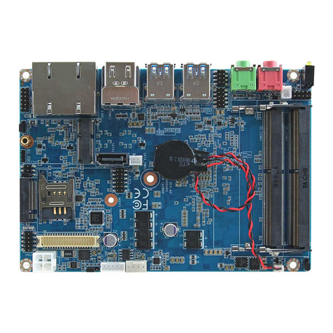
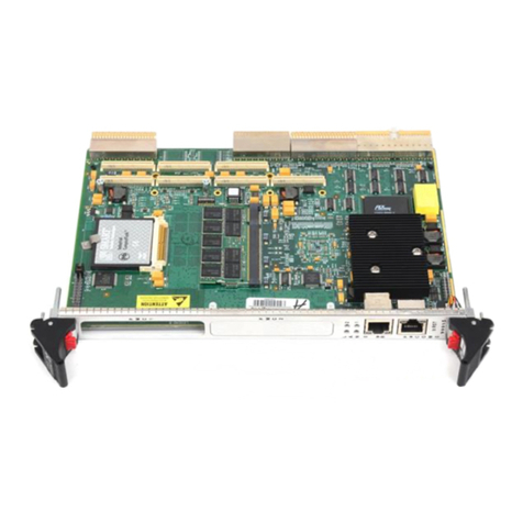
Acrosser Technology AR-B1842-G User manual

AR-B1842-G
Socket 479 Pentium®M
INDUSTRIAL GRADE
CPU BOARD
User’ s Guide
Edition: 2.01
Book Number: AR-B1842-07.0115

2
Table of Contents
0. PREFACE.................................................................................................................................................................... 3
0.1 COPYRIGHT NOTICE AND DISCLAIMER.....................................................................................................................................3
0.2 WELCOME TO THE AR-B1842-G CPU BOARD............................................................................................................................3
0.3 BEFORE YOU USE THIS GUIDE...................................................................................................................................................3
0.4 RETURNING YOUR BOARD FOR SERVICE.................................................................................................................................3
0.5 TECHNICAL SUPPORT AND USER COMMENTS........................................................................................................................3
0.6 STATIC ELECTRICITY PRECAUTIONS ........................................................................................................................................4
1. INTRODUCTION.......................................................................................................................................................... 5
1.1 PACKING LIST................................................................................................................................................................................5
1.2 SPECIFICATIONS...........................................................................................................................................................................6
1.3 BLOCK DIAGRAM...........................................................................................................................................................................7
2. INSTALLATION........................................................................................................................................................... 8
2.1 AR-B1842-G'S BOARD DIMENSIONS ...........................................................................................................................................8
2.2 CPU INSTALLATION ......................................................................................................................................................................9
2.3 MEMORY INSTALLATION (DDR2 SODIMM MEMORY SIZE) ....................................................................................................10
2.4 POWER INSTALLATION ..............................................................................................................................................................10
3. CONNECTION........................................................................................................................................................... 11
3.1 PS/2 KEYBOARD & MOUSE(CN1).......................................................................................................................................11
3.2 KEYBOARD & MOUSE HEADER (J6)..........................................................................................................................................11
3.3 KEYBOARD LUCK/UNLCK HEADER (JP5).................................................................................................................................11
3.4 SERIAL PORT CONNECTOR(COM1).....................................................................................................................................11
3.5 INTERNAL SERIAL PORT HEADER (COM2)........................................................................................................................11
3.6 COM2 FOR RS232 / RS422 / RS485 SELECT (JP3).............................................................................................................12
3.7 RS422 / RS485 HEADER(J8)...................................................................................................................................................12
3.8 IRDA HEADER(J4)................................................................................................................................................................12
3.9 VGA CONNECTOR(VGA1)......................................................................................................................................................12
3.10 ETHERNET RJ-45 CONNECTOR(LAN1)..............................................................................................................................12
3.11 PARALLEL PORT HEADER(J2)............................................................................................................................................13
3.12 CPU FREQUENCY SELECT TABLE (J10)..............................................................................................................................13
3.13 HARD DISK CONNECTOR (IDE1) .............................................................................................................................................13
3.14 COMPACT FLASH CONNECTOR(CF1)................................................................................................................................14
3.15 COMPACT FLASH CONNECTOR MASTER∕SLAVE SELECT HEADER(JP6)..................................................................14
3.16 AUDIO LINE IN / LINE OUT / MIC HEADER (AUDIO1)........................................................................................................14
3.17 CD IN HEADER(J1)................................................................................................................................................................15
3.18 CPU FAN POWER CONNECTOR(FAN1, FAN2)..................................................................................................................15
3.19 COMS BATTERY HEADER(JP4)...........................................................................................................................................15
3.20 18, 24 BITS LVDS CONNECTOR(LCD1)..............................................................................................................................15
3.21 LVDS INTERVER CONNECTOR(LCDPW1)..........................................................................................................................15
3.22 USB PORT HEADER (USB1, USB2)....................................................................................................................................16
3.23 DDR2 SOCKET(DDR2SODIMM1).........................................................................................................................................16
3.24 MINI PCI SLOT(MINIPCI1).....................................................................................................................................................16
3.25 SATA CONNECTOR(SATA1, SATA2)...................................................................................................................................16
3.26 GPIO PORT HEADER(J9)......................................................................................................................................................16
3.27 CPU VOLTAGE SELECT HEADER(JP1)..............................................................................................................................16
3.28 PROTECT U HEADER(JP2)..................................................................................................................................................17
3.29 PANEL HEADER(J3)..............................................................................................................................................................17
3.30 AT POWER CONNECTOR(PW1)..........................................................................................................................................17
4. WATCHDOG TIMER CONFIGURATION.................................................................................................................. 18
4.1 WATCHDOG TIMER SETTING ....................................................................................................................................................18
5. BIOS CONSOLE........................................................................................................................................................ 20
5.1 MAIN SETUP.................................................................................................................................................................................20
5.2 ADVANCED CHIPSET SETUP.....................................................................................................................................................22
5.3 POWER SETUP............................................................................................................................................................................23
5.4 PERIPHERALS SETUP ................................................................................................................................................................24
5.5 PNP/PCI SETUP...........................................................................................................................................................................26
5.6 PC HEALTH SETUP .....................................................................................................................................................................27
5.7 BOOT SETUP ...............................................................................................................................................................................28
5.8 EXIT SETUP..................................................................................................................................................................................29
5.9 BIOS UPDATE ..............................................................................................................................................................................30
APPENDIX A. ADDRESS MAPPING............................................................................................................................ 31
IO ADDRESS MAP..............................................................................................................................................................................31
APPENDIX B. INTERRUPT REQUEST (IRQ)............................................................................................................... 32

3
0. PREFACE
0.1 COPYRIGHT NOTICE AND DISCLAIMER
This document is copyrighted, 2006, by Acrosser Technology Co., Ltd. All rights are reserved. No part
of this manual may be reproduced, copied, transcribed, stored in a retrieval system, or translated into
any language or computer language in any form or by any means, such as electronic, mechanical,
magnetic, optical, chemical, manual or other means without the prior written permission or original
manufacturer.
Acrosser Technology assumes no responsibility or warranty with respect to the content in this manual
and specifically disclaims any implied warranty of merchantability or fitness for any particular purpose.
Furthermore, Acrosser Technology reserves the right to make improvements to the products described
in this manual at any times without notice. Such revisions will be posted on the Internet
(WWW.ACROSSER.COM) as soon as possible.
Possession, use, or copy of the software described in this publication is authorized only pursuant to
valid written license from Acrosser or an authorized sub licensor.
ACKNOWLEDGEMENTS
Acrosser,AMI, IBM PC/AT, ALI, Windows 3.1, MS-DOS…are registered trademarks.
All other trademarks and registered trademarks are the property of their respective owners.
0.2 WELCOME TO THE AR-B1842-G CPU BOARD
This guide introduces the Acrosser AR-B1842-G CPU Board.
Use information provided in this manual describes this card’s functions and features. It also helps you
start, set up and operate your AR-B1842-G. General system information can also be found in this
publication.
0.3 BEFORE YOU USE THIS GUIDE
Please refer to the Chapter 3, “Setting System,” in this guide, if you have not already installed this
AR-B1842-G. Check the packing list before you install and make sure the accessories are completely
included.
AR-B1842-G CD provides the newest information regarding the CPU card. Please refer to the files of
the enclosed utility CD. It contains the modification and hardware & software information, and adding
the description or modification of product function after manual printed.
0.4 RETURNING YOUR BOARD FOR SERVICE
If your board requires any services, contact the distributor or sales representative from whom you
purchased the product for service information. If you need to ship your board to us for service, be sure
it is packed in a protective carton. We recommend that you keep the original shipping container for this
purpose.
You can help assure efficient servicing for your product by following these guidelines:
1. Include your name, address, daytime telephone, facsimile number and E-mail.
2. A description of the system configuration and/or software at the time of malfunction.
3. A brief description of the problem occurred.
0.5 TECHNICAL SUPPORT AND USER COMMENTS
Users comments are always welcome as they assist us in improving the quality of our products and the
readability of our publications. They create a very important part of the input used for product
enhancement and revision.
We may use and distribute any of the information you provide in any way appropriate without incurring
any obligation. You may, of course, continue to use the information you provide.
If you have any suggestions for improving particular sections or if you find any errors on it, please send
your comments to Acrosser Technology Co., Ltd. or your local sales representative and indicate the
manual title and book number.
Internet electronic mail to: Sales@acrosser.com

4
0.6 STATIC ELECTRICITY PRECAUTIONS
Before removing the board from its anti-static bag, read this section about static electricity precautions.
Static electricity is a constant danger to computer systems. The charge that can build up in your body
may be more than sufficient to damage integrated circuits on any PC board. It is, therefore, important to
observe basic precautions whenever you use or handle computer components. Although areas with
humid climates are much less prone to static build-up, it is always best to safeguard against accidents
that may result in expensive repairs. The following measures should be sufficient to protect your
equipment from static discharge:
Touch a grounded metal object to discharge the static electricity in your body (or ideally, wear a
grounded wrist strap).
When unpacking and handling the board or other system components, place all materials on an
anti-static surface.
Be careful not to touch the components on the board, especially the “golden finger” connectors on
the bottom of the board.

5
1. INTRODUCTION
Welcome to the AR-B1842-G Embedded AT/ATX Single Board Computer. The AR-B1842-G Pentium®
M embedded board incorporates the Intel®advanced 915GME Chipset that supports processors from
600MHz to 2.0MHz in 478-ball Micro-FCBGA package with a front side bus of 400/533MHz.
Graphics display functionality is provided by Build-in Intel Graphics Media Accelerator(GMA) that
supports CRT display and LVDS interface with 2X18-bit panel specifications. Ethernet connectivity
comes from the ICH6M-integrated Ethernet 10/100 Ethernet controller.
One DDR II SO-DIMM sockets supports up to 1GB of memory. Two Serial and two SATA ports are
supported. There is one IDE connectors – IDE1 supporting UDMA33/66/100 while supporting a CF
Type II socket for its slave channel.
Other I/O features include four USB ports connector with pin headers. Expansion slots composed of
one Mini PCI slot. AR-B1842-G uses a 20-pin ATX power and a big 4-pin AT input connector.
1.1 PACKING LIST
In addition to this User's Manual, the AR-B1842-G package includes the following items:
The quick setup manual
1 AR-B1842-G CPU board
1 Software utility CD
1 5.25” IDE HDD ATA 100Cable
1 Audio interface Cable
1 Serial port Cable
1 Print port Cable
1 PS2 to PS2 Y Cable
1 JST to PS2 Y Cable(optional)
1 USB ports on one bracket Cable
1 SATA cable

6
1.2 SPECIFICATIONS
Model Name AR-B1842-G V 2.0
Product
Descriptions PCI-E Half Size Pentium M CPU card with Intel 915GME chipset, VGA, 10/100 LAN,
CF, Mini PCI, 2 Serial ports, 4 USB 2.0
General Note
CPU Grade Socket 478 FSB533/400 MHz Pentium M/ Celeron M (90nm
and 130nm)
CPU Fan Slim Cooling Fan with on board fan power connector
BIOS AWARD
System Chipsets Intel 915GME + ICH6M
System Memory DDR2 SDRAM SO-DIMM socket x1
Maximum up to 1GB
Watchdog Timer Software programmable 1~63 Seconds
Battery Lithium Battery, 3V 220mAH
Power
Requirements
AT/ATX
Need independent 5V/12V input by 2x5 pin connector Big 4 pin
Hardware
monitoring 1. CPU voltage
2. CPU Temperature
3. Voltage Monitoring
BIOS Support
OS DOS, WinCE, Linux Fedora 2.6.4/Redhat 2.4.x and above, Win
2000/XP, XPe
Video
Video Interface Build-in Intel Graphics Media Accelerator(GMA)
CRT 1 x VGA port D-Sub15
LVDS 18-bits LVDS Interface
LCD inverter power connector and ON/OFF control Support
3.3V
DF13
Audio
Audio Interface AC97 Codec, Realtek ALC 655, Line out
L/R Channel
Storage
IDE 1 x 40 pin IDE connector supports Ultra DMA 2x20x2.54mm
SSD 1 x Compact Flash support UDMA
Socket upward and CF surface with PCB Edge Type-II
Socket
SATA 2 x SATA connectors
Network Interface
Ethernet 1 x Intel 82562EZ (10/100 Mbps)
Support PXE function boot from LAN and Wake on LAN RJ-45
connector
I/O
Super I/O Winbond 83627EHG
Serial Port COM1 on board DB-9 (RS-232)
COM2 2 x10 pin head support RS-232/422/485 DB-9
Pin Header
Parallel Port On board 1 x 26 pin head for LPT1, support SPP/EPP/ECP
modes Pin header
GPIO 8 bit independent I/O Lines, TTL level Pin Header
USB 4 x USB 2.0 Pin Header
IrDA 1 x 4 x 2.5mm pin head (SIR mode) Pin Header
Audio Line out (L/R Channel) Pin Head
Expansion slot 1 x Mini PCI slot Slot
Keyboard
Mouse 1 x PS/2 for Keyboard and Mouse Mini Din
Pin head
Buzzer
Mechanical
Dimension 167mm x 121mm

7
Operating
Temperature 0~60oC (32~140oF)
Storage
Temperature -20~80oC (-4~176oF)
Relative Humidity 0 to 90% @ 45°C, non-condensing
EMC & Safety
EMC CE , FCC Class A
Safety N/A
1.3 BLOCK DIAGRAM
PRINTER Port
(533Mhz)*(8byte)=4.2GB/s
( pin header)
PS/2 KB/MS D-type
R,G,B (10)
IMVP_IV
DDR2 533/400
FSB 133 Mhz core clock
DDR2 SDRAM SO-DIMM X 1
PCI-E 8X Golden
Finger (1X4) Mini PCI Slot
LPC
FWH
Bios
2M Cache
DEF:4eh
GMCH Alviso
DDR2 BUS(2)
non-ECC
USB 4 Port
4 port with pin header
AC'97/Azalia
609 BGA
TV OUT
FW82801FBM
USB2.0(8)
Dothan Processor
DMI(direction media interface)
Serial ATA x2
Intel U21
82562ET
LVDS DUAL CH
Com1(RS232),
1257 PCBGA
Com2(RS232)
LAN Diff(7)
PCI-E Bus(3)
Express port
LVDS (9)
single 1GB
( pin header)
ICH6M
(533Mhz)*(16byte)=8.5GB/s
( pin header)
LAN PHY(6)
PCI Bus(6)
10/100 M LAN
(*1)x4
CRT D-type CONN
UDMA (40PIN/2.5mm)
& CF Card
SATA BUS(5)
PCI-E Bus(3)
CHANNEL A
USB 2.0 (8)
LPC
915GM
4 Lanes
Super I/O
AC97 codec ALC655
HOST BUS(1)
LAN1
RJ45
LPC/IF
Game port
SATA(2)
2005/09/21
2 GB/s point-to-point DMI to ICH6
(400Mhz)*(16byte)=6.4GB/s
PCI-E 16X
Golden
Finger
IrDA X1
8 bits GPI/O
ATA100(1)
(each direction 1GB/s)
HUB LINK(4)
( 9pin Connector )
478 uFCPGA
W83627EHF
(Line-out,Line-in,Mic.)
533 MT/s(133Mhz core clock)

8
2. INSTALLATION
This chapter describes how to install theAR-B1842-G.At first, the layout of AR-B1842-G is shown, and
the unpacking information that you should be careful is described. The jumpers and switches setting for
the AR-B1842-G’s configuration are as below.
2.1 AR-B1842-G'S BOARD DIMENSIONS

9
2.2 CPU INSTALLATION
The AR-B1842-G embedded board supports a Socket 478 processor socket for Intel®Pentium®M or
Celeron®M processors.
The processor socket comes with a screw to secure the processor. As shown in the left picture below,
loosen the screw first before inserting the processor. Place the processor into the socket by making sure
the notch on the corner of the CPU corresponds with the notch on the inside of the socket. Once the
processor has slide into the socket, fasten the screw. Refer to the figures below.
After you have installed the processor into the socket, check if the jumpers for the CPU type and speed are correct.

10
2.3 MEMORY INSTALLATION (DDR2 SODIMM MEMORY SIZE)
The AR-B1842-G board supports DDR2 400/533 MHz main memory. One 200-pin SODIMM connector on the
board supports unbufferedm nonECC, single and double-side DDR2 400/533 MHz SODIMMs. These SODIMMs
provide the ability to use up to maximum of 1 GBytes system memory.
To install the DDR2 modules, locate the memory slot on the embedded board and perform the following
steps:
1. Hold the DDR2 module so that the key of the DDR2 module align with those on the memory slot.
2. Gently push the DDR2 module in an upright position until the clips of the slot close to hold the DDR2
module in place when the DDR2 module touches the bottom of the slot.
3. To remove the DDR2 module, press the clips with both hands.
2.4 POWER INSTALLATION
The AR-B1842-G collocates with AR-MB3E-G, because there is no 3.3V power input on AR-B1842-G
board. To install the power ofAR-B1842-G, please see the install diagram.
Note: No matter what power input you select (AT or ATX), the big 4-pin power connector always need
+12V, +5V power input.

11
3. CONNECTION
The connectors on AR-B1842-G allows you to connect external devices such as USB devices, serial
port drives, hard disk devices, printers, etc. The following table lists the connectors on AR-B1842-G
and their respective functions.
3.1 PS/2 KEYBOARD & MOUSE(CN1)
3.2 KEYBOARD & MOUSE HEADER (J6)
3.3 KEYBOARD LUCK/UNLCK HEADER (JP5)
3.4 SERIAL PORT CONNECTOR(COM1)
3.5 INTERNAL SERIAL PORT HEADER (COM2)
PIN SIGNAL PIN SIGNAL
1 KBDAT 2 MSDAT
3 GND 4 +5V
5 KBCLK 6 MSCLK
PIN SIGNAL PIN SIGNAL
1 KBDAT 2 MSDAT
3 GND 4 +5V
5 KBCLK 6 MSCLK
PIN SIGNAL PIN SIGNAL
1 DCD1 6 DSR1
2 RXD1 7 RTS1
3 TXD1 8 CTS1
4 DTR1 9 RI1
5 GND
PIN SIGNAL PIN SIGNAL
1 DCD2 2 DSR2
3 RXD2 4 RTS2
5 TXD2 6 CTS2
7 DTR2 8 RI2
9 GND 10 GND

12
3.6 COM2 FOR RS232 / RS422 / RS485 SELECT (JP3)
1 2
65
3.7 RS422 / RS485 HEADER(J8)
1 4
3.8 IRDA HEADER(J4)
1 5
3.9 VGA CONNECTOR(VGA1)
3.10 ETHERNET RJ-45 CONNECTOR(LAN1)
PIN SIGNAL
1-2 ON RS232
(Factory Preset)
3-4 ON RS422
5-6 ON RS485
PIN SIGNAL
1 TX2+
2 TX2-
3 RX2+
4 RX2-
PIN SIGNAL PIN SIGNAL
1 +5V 2 N.C
3 IRRX 4 GND
5 IRTX
PIN SIGNAL PIN SIGNAL
1 RED 9 VCC
2 GREEN 10 GND
3 BLUE 11 N.C.
4 N.C. 12 VGADATA
5 GND 13 HSYNC
6 GND 14 VSYNC
7 GND 15 VGACLK
8 GND
PIN SIGNAL PIN SIGNAL
1 TX+ 2 TX-
3 RX+ 4 N.C.
5 N.C. 6 RX-
7 N.C. 8 N.C.

13
3.11 PARALLEL PORT HEADER(J2)
3.12 CPU FREQUENCY SELECT TABLE(J10)
3.13 HARD DISK CONNECTOR (IDE1)
1 39
2 40
PIN SIGNAL PIN SIGNAL
1 STB# 14 AFD#
2 PD0 15 ERROR#
3 PD1 16 INIT#
4 PD2 17 SLIN#
5 PD3 18 GND
6 PD4 19 GND
7 PD5 20 GND
8 PD6 21 GND
9 PD7 22 GND
10 ACK# 23 GND
11 BUSY 24 GND
12 PE 25 GND
13 SLCT 26 N.C.
PIN CPU_HOST_FREQUENCY
4_6,1_3 100MHz【BANIAS】
4_6,3_5 133MHz【DOTHAN】
PIN SIGNAL PIN SIGNAL
1 /RESET 2 GND
3 PDATA7 4 PDATA8
5 PDATA6 6 PDATA9
7 PDATA5 8 PDATA10
9 PDATA4 10 PDATA11
11 PDATA3 12 PDATA12
13 PDATA2 14 PDATA13
15 PDATA1 16 PDATA14
17 PDATA0 18 PDATA15
19 GND 20 N.C.
21 PDDREQ 22 GND
23 /PDIOW 24 GND
25 /PDIOR 26 GND
27 PIORDY 28 GND
29 /PDDACK 30 GND
31 IRQ14 32 N.C.
33 PDA1 34 P66DET
35 PDA0 36 PDA2
37 /PDCS1 38 /PDCS3
39 HDDLED 40 GND
1
2
5
2
4
6

14
3.14 COMPACT FLASH CONNECTOR(CF1)
50 1
NOTE: Compact flash (CF1) and IDE1 share the same IDE
channel. Since a compact flash card is installed, the IDE
device will become unstable. CF card and IDE1 cannot use at
the same time.
3.15 COMPACT FLASH CONNECTOR MASTER⁄SLAVE SELECT HEADER(JP6)
1
3.16 AUDIO LINE IN / LINE OUT / MIC HEADER (AUDIO1)
1 13
2 14
PIN SIGNAL PIN SIGNAL
1 GND 2 PDATA3
3 PDATA4 4 SDATA5
5 PDATA6 6 SDATA7
7 /PDCS1 8 GND
9 GND 10 GND
11 GND 12 GND
13 +5V 14 GND
15 GND 16 GND
17 GND 18 PDA2
19 PDA1 20 PDA0
21 PDATA0 22 PDATA1
23 PDATA2 24 GND
25 GND 26 GND
27 PDATA11 28 PDATA12
29 PDATA13 30 PDATA14
31 PDATA15 32 /PDCS3
33 GND 34 /PDIOR
35 /PDIOW 36 +5V
37 IRQ14 38 +5V
39 M/S
SELECT 40 N.C.
41 /RESET 42 PIORDY
43 N.C. 44 +5V
45 HDDLED 46 N.C.
47 PDATA8 48 PDATA9
49 PDATA10 50 GND
PIN SIGNAL
1-2 ON MASTER MODE
1-2 OFF SLAVE MODE
PIN SIGNAL PIN SIGNAL
1 MICIN2 2 LIN_L
3 N.C 4 LIN_R
5 +12V 6 VCC
7 LOUT_L 8 MICIN1
9 LOUT_R 10 PCBEEP
11 GND 12 GND
13 GND 14 GND

15
3.17 CD IN HEADER(J1)
1 4
3.18 CPU FAN POWER CONNECTOR(FAN1, FAN2)
1
3.19 COMS BATTERY HEADER(JP4)
1
3.20 18 BITS LVDS CONNECTOR(LCD1)
3.21 LVDS INTERVER CONNECTOR(LCDPW1)
PIN SIGNAL
1 CD-L
2 GND
3 GND
4 CD-R
PIN SIGNAL
1 GND
2 +12V
3 SENSE
PIN SIGNAL
1-2 ON NORMAL OPERATION
(Factory Preset)
2-3 ON CLEAR CMOS
PIN SIGNAL PIN SIGNAL
1 LVDS_PWR 2 GND
3 LVDS_CLKBN 4 LVDS_CLKBP
5 GND 6 LVDS_YBN2
7 LVDS_YBP2 8 GND
9 LVDS_YBN1 10 LVDS_YBP1
11 N.C. 12 N.C.
13 LVDS_YBP0 14 LVDS_YBN0
15 GND 16 RXOC+
17 LVDS_CLKAN 18 GND
19 LVDS_YAP2 20 LVDS_YAN2
21 DDPCLK 22 LVDS_YAP1
23 LVDS_YAN1 24 DDPDATA
25 LVDS_YAP0 26 LVDS_YAN0
27 N.C. 28 N.C.
29 LVDS_PWR 30 LVDS_PWR
PIN SIGNAL PIN SIGNAL
1 +12V 4 LVDS_BKLTEN
2 +12V 5 GND
3 GND 6 LVDS_BKLTCL

16
3.22 USB PORT HEADER (USB1, USB2)
3.23 DDR2 SOCKET(DDR2SODIMM1)
3.24 MINI PCI SLOT(MINIPCI1)
3.25 SATA CONNECTOR(SATA1, SATA2)
17
3.26 GPIO PORT HEADER(J9)
3.27 CPU VOLTAGE SELECT HEADER(JP1)
1
PIN SIGNAL PIN SIGNAL
1 VCC 5 GND
2 DATA- 6 DATA+
3 DATA+ 7 DATA-
4 GND 8 VCC
PIN SIGNAL PIN SIGNAL
1 GND 5 SATA RXP
2 SATATXP 6 SATARXN
3 SATATXN 7 GND
4 GND
PIN SIGNAL PIN SIGNAL
1 GND 6 OUT0
2 VCC 7 IN 3
3 OUT 3 8 IN 1
4 OUT 1 9 IN 2
5 OUT 2 10 IN 0
PIN SIGNAL
1-2 ON FORFSB133
【DOTHAN】
1-2 OFF FOR FSB100
【BANIAS】
(Factory Preset)

17
3.28 PROTECT U HEADER(JP2)
1 3
3.29 PANEL HEADER(J3)
3.30 AT POWER CONNECTOR(PW1)
PIN SIGNAL
1-2 ON WRITER FUNCTION
2-3 ON READ FUNCTION
(Factory Preset)
PIN SIGNAL
1-2 POWER LED
3-4 HDD LED
5-6 SPEAKER
7-8 RESET BUTTON
9-10 POWER BUTTON

18
4. WATCHDOG TIMER CONFIGURATION
4.1 WATCHDOG TIMER SETTING
The WDT (Watch Dog Timer) is used to generate a variety of output signals after a user programmable
count. The WDT is suitable for use in the prevention of system lock-up, such as when software becomes
trapped in a deadlock. Under these sorts of circumstances, the timer will count to zero and the selected
outputs will be driven. Under normal circumstance, the user will restart the WDT at regular intervals
before the timer counts to zero.
The watchdog timer is a circuit that maybe used from your program software to detect crash or hang up.
The Watchdog timer is automatically disabled after reset. Once you enabled the watchdog timer, your
program should trigger the watchdog timer every time before it times out. After you trigger the watchdog
timer, the timer will be set to zero and start to count again. If your program fails to trigger the watchdog
timer before times out, it will generate a reset pulse to reset the system or trigger the IRQ 9 signal in
order to tell your system that the watchdog time is out.
User could test watchdog function under ‘Debug’ program as follows:
C:>debug
o 4E 87 ;Extended Functions Enable Register
o 4E 87 ;Extended Functions Enable Register
o 4E 07 ;EFIR=EFER (Extended Functions Index Register)
point to Logical Device Number Reg.
o 4F 08 ; Select logical device 8, (Watchdog Function)
o 4E 30 ; Device Active register
o 4F01 ;update CR30 with value 01H
o 4E F6 ; Select Watchdog count mode seconds or minutes
o 4F 08 ;update CRF6 with value 08H ,(8sec reset)
q

19
Sample code as below:
IO_Port_Address = 0x4E;
outportb(IO_Port_Address,0x87); // (EFER) Extended Functions Enable Register
outportb(IO_Port_Address,0x87);
outportb(IO_Port_Address,0x2D); // Point to Global Reg.
// Select Multi-Function pin, (Bit0=0 Watchdog Function)
outportb(IO_Port_Address+1,(inportb(IO_Port_Address+1)&0xFE));
outportb(IO_Port_Address,0x07); // Point to Logical Device Number Reg.
outportb(IO_Port_Address+1,0x08); // Select logical device 8, (Watchdog Function)
outportb(IO_Port_Address,0x30); // Device Active register
outportb(IO_Port_Address+1,0x01);
outportb(IO_Port_Address,0xF5); // Select Watchdog count mode seconds or minutes
outportb(IO_Port_Address+1,Format); // Default is second
outportb(IO_Port_Address,0xF6); // Set Watchdog Timer Value
outportb(IO_Port_Address+1,Time);// 0x00 to disable, max 0xFF

5. BIOS CONSOLE
This chapter describes the AR-B1842-G BIOS menu displays and explains how to perform common
tasks needed to get up and running, and presents detailed explanations of the elements found in each
of the BIOS menus. The following topics are covered:
Main Setup
Advanced Chipset Setup
Power Setup
Peripherals Setup
PnP/PCI Setup
PC Health Setup
Boot Setup
Exit Setup
5.1 MAIN SETUP
The <Main Setup> choice allows you to record some basic hardware configuration in your computer
system and set the system clock and error handling. If the motherboard is already installed in a working
system, you will not need to select this option. You will need to run this Setup option, however, if you
change your system hardware configuration, the onboard battery fails, or the configuration stored in the
COMS memory was lost or damaged.
Setup Main Menu
About the button of the menu are the control keys for use on this menu. If you need any help in each
item field, you can press the <F1>key, It will display the relevant information to help you. The
memory display at the automatically according to the memory changed. The following describes each
item of this menu.
Date Setup
The date format is:
DAY:SUN to SAT
Table of contents
Other Acrosser Technology Single Board Computer manuals
Acrosser Technology
Acrosser Technology AR-B1641 User manual
Acrosser Technology
Acrosser Technology AR-B1684VSL2 User manual
Acrosser Technology
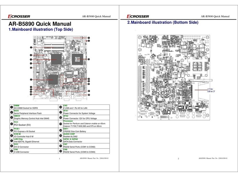
Acrosser Technology AR-B5890 Installation guide
Acrosser Technology
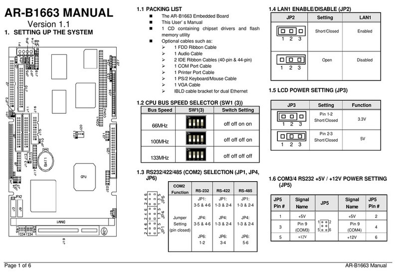
Acrosser Technology AR-B1663 User manual
Acrosser Technology
Acrosser Technology AR-B1831 User manual
