AMS AS3930 User manual

AS3930 Standard Board
ams Demo Kit Manual, Confidential
Page 2
[v1-02] 2014-Jul-10
Document Feedback
Table of Contents
1Introduction .......................................................................................................................... 4
1.1 Kit Content ........................................................................................................................... 4
2Getting Started..................................................................................................................... 4
3Hardware Description........................................................................................................... 5
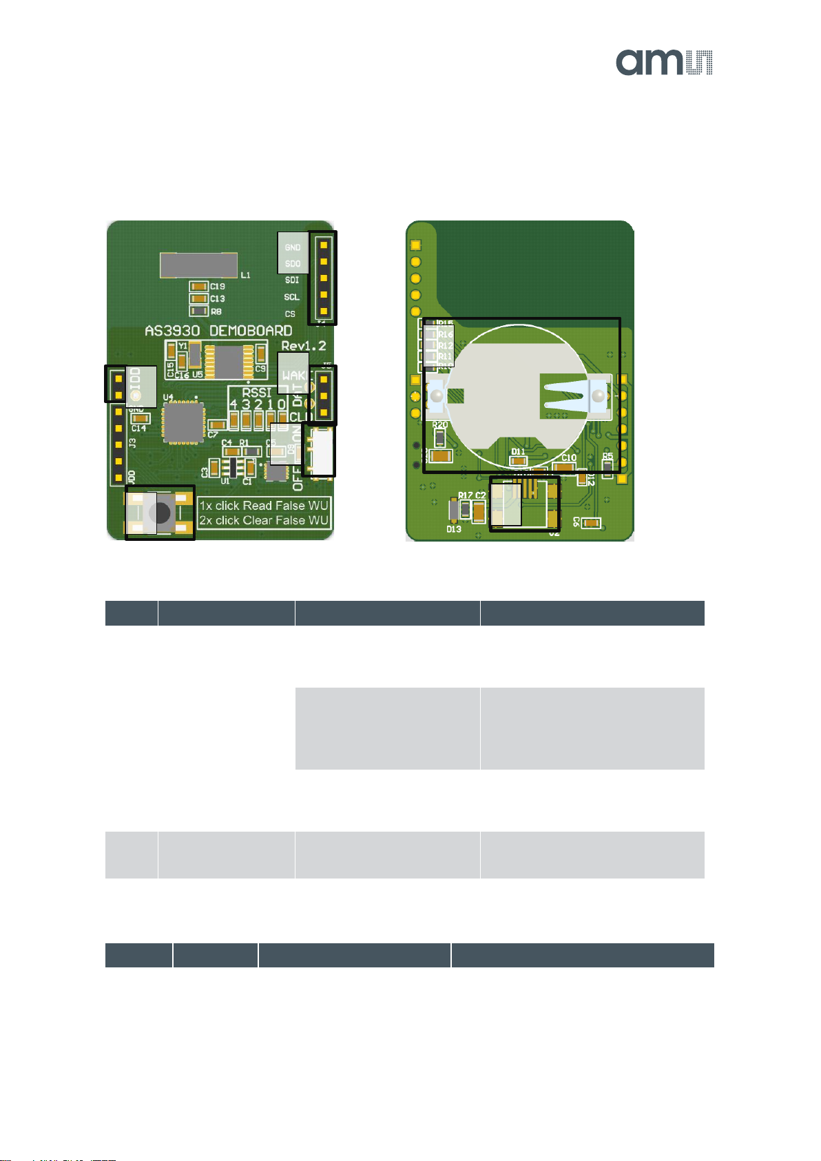
3.1 AS3930 Demoboard Description ......................................................................................... 5
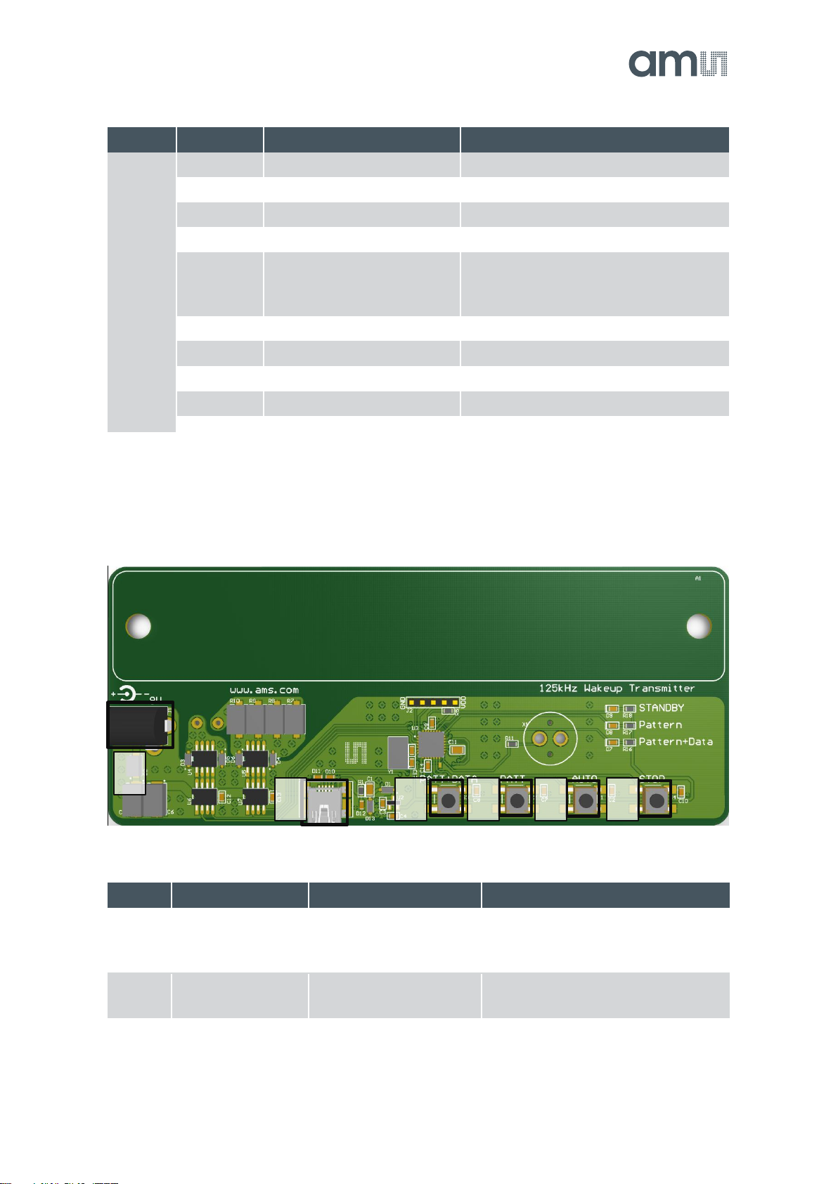
3.2 125 kHz Wakeup Transmitter Board.................................................................................... 6
4Software Description............................................................................................................ 7
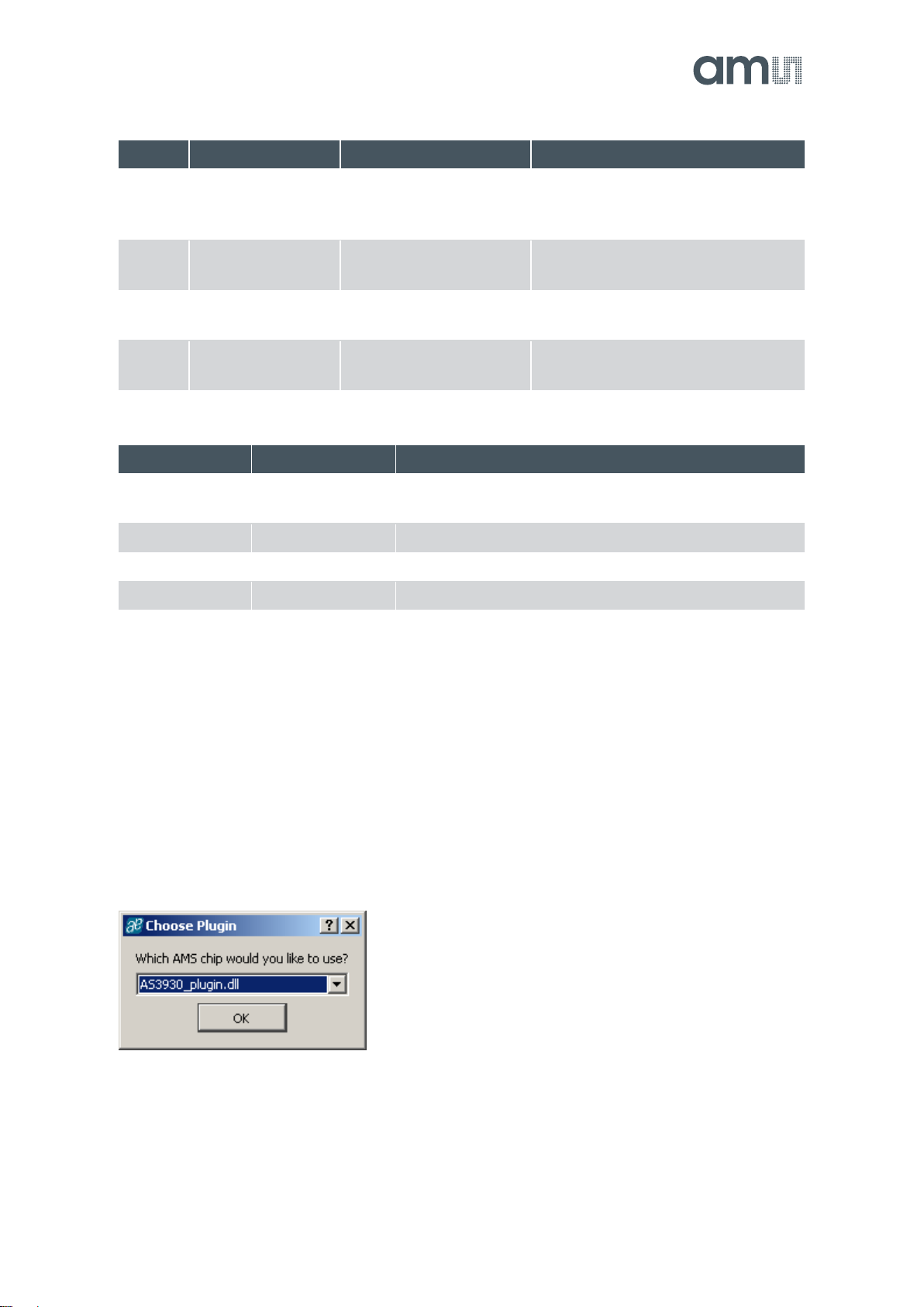
4.1 Install the GUI ...................................................................................................................... 7
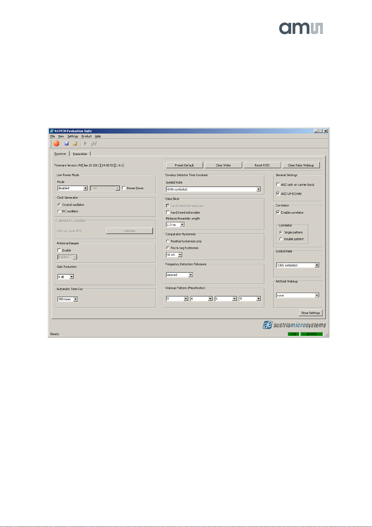
4.2 Description of the GUI of the Receiver ................................................................................ 8
4.2.1 Settings Description............................................................................................................. 9
4.2.1.1 Low Power Mode ................................................................................................................. 9
4.2.1.2 Clock Generator................................................................................................................... 9
4.2.1.3 Calibrate RC Oscillator ........................................................................................................ 9
4.2.1.4 Antenna Damper.................................................................................................................. 9
4.2.1.5 Gain Reduction .................................................................................................................... 9
4.2.1.6 Automatic Time-Out............................................................................................................. 9
4.2.1.7 Envelope Detector Time Constant....................................................................................... 9
4.2.1.8 Data Slicer............................................................................................................................ 9
4.2.1.9 Comparator Hysteresis ......................................................................................................10
4.2.1.10 Frequency Detection Tolerance.........................................................................................10
4.2.1.11 Wakeup Pattern (Manchester)........................................................................................... 10
4.2.1.12 General Settings ................................................................................................................ 10
4.2.1.13 Correlator ...........................................................................................................................10
4.2.1.14 Symbol Rate....................................................................................................................... 10
4.2.1.15 Artificial Wakeup ................................................................................................................ 10
4.2.1.16 Clear Wake ........................................................................................................................ 10
4.2.1.17 Reset RSSI ........................................................................................................................ 10
4.3 Clear False Wakeup........................................................................................................... 11
4.4 Description of the GUI for the Wake-up Transmitter Board............................................... 11
4.4.1 Settings Description...........................................................................................................11
4.4.1.1 Duration of Carrier Burst....................................................................................................11
4.4.1.2 Number of Preamble Symbols........................................................................................... 12
4.4.1.3 Symbol Rate....................................................................................................................... 12
4.4.1.4 Enable Buzzer....................................................................................................................12

AS3930 Standard Board
ams Demo Kit Manual, Confidential
Page 3
[v1-02] 2014-Jul-10
Document Feedback
4.4.1.5 Wake-up Pattern (Manchester)..........................................................................................12
4.4.1.6 Manchester Pattern Length................................................................................................ 12
4.4.1.7 Correlator ...........................................................................................................................12
5Schematics, Layers and BOM ........................................................................................... 13
5.1 AS3930 Demoboard Schematic.........................................................................................13
5.2 AS3930 Demoboard Layout - Top and Bottom Layer........................................................ 14
5.3 AS3930 Demoboard BOM ................................................................................................. 15
5.4 125 kHz Wake-up Transmitter Board Schematic...............................................................16
5.5 125 kHz Wake-up Transmitter Board Layout..................................................................... 17
5.6 125 kHz Wake-up Transmitter Board BOM .......................................................................17
6Ordering & Contact Information.........................................................................................18
7Copyrights & Disclaimer.....................................................................................................19
8Revision Information .......................................................................................................... 20

AS3930 Standard Board
ams Demo Kit Manual, Confidential
Page 4
[v1-02] 2014-Jul-10
Document Feedback
1 Introduction
The AS3930 Demo Board demonstrates the main features of the AS3930. These include 1D wake-
up pattern detection, readout of false wake-ups, possibility to measure current consumption in
different operating modes, and measurement access to SPI communication and data output.
Additional features are accessible via USB through the GUI that was developed for easy access to
the register map. Features such as the programmable wake-up pattern, adjustable sensitivity level,
low power listening modes and several more can be programmed via the GUI. The influence
different settings have on the detection efficiency can be observed right away by using the 125 kHz
Wake-up Transmitter Board.
1.1 Kit Content
The AS3930 Demo Kit contains the following items:
1x AS3930 Demo Board
1x 125kHz Wake-up Transmitter Board
1x 9V power supply
2x CR2032 Coin Cell
1x USB stick
1x USB Cable
2 Getting Started
Connect the +9V DC Power Supply at “F” on the 125 kHz Wake-up Transmitter Board.
Start to transmit Wake-up Patterns via AUTO “C” or PATTERN “B”.
Insert the +3V Battery at “H” of the AS3930 Demo Board.
Turn on the AS3930 Demo Board via the ON/OFF –switch “C”. When turning on the boards all
indication-LEDs flash up once.
As soon as the AS3930 Demo Board receives a Wake-up Pattern, the RSSI LEDs flash up for
0.5s and show the actual Received Signal Strength.

AS3930 Standard Board
ams Demo Kit Manual, Confidential
Page 5
[v1-02] 2014-Jul-10
Document Feedback
3 Hardware Description
3.1 AS3930 Demoboard Description
Figure 1: AS3930 Demoboard Description Top and Bottom
Figure 2: User Interface Description
Label
Name
Description
Info
A
BUTTON
1x short press reads the
false wake-ups
The number of false wake-ups
can be read out and are displayed
via the RSSI –LEDs.
2x short press (double
click) clears the false wake-
ups
Pressing FALSE WAKEUP two
times resets the number of false
wake-ups. Each RSSI –LED is
turned on shortly.
C
ON/OFF
ON/OFF –Switch
Power on/off the demoboard.
Source (Battery or USB) is
automatically detected.
G
USB –
Connector
Mini USB 5-pin connector
USB Interface for the GUI
H
CR2032 BATTERY
Battery Holder
Insert CR2032 here.
Figure 3: Jumper Description
Jumper
Name
Description
Info
F
IDD
Supply Current
The supply current of the AS3930 can
be measured. Set this jumper for normal
operation.
A
C
D
E
F
H
G

AS3930 Standard Board
ams Demo Kit Manual, Confidential
Page 6
[v1-02] 2014-Jul-10
Document Feedback
Jumper
Name
Description
Info
D
AS3930 specific outputs
D1
WAKE
Wake Output Interrupt
D2
DAT
Data Output
D3
CL_DAT
Manchester Recovered Clock
E
Microcontroller - Interface
The SDI –Interface from the
microcontroller can be replaced by a
proprietary solution
E1
CS
Serial Digital Interface Chip Select
E2
SCL
Serial Digital Interface Clock
E3
SDI
Serial Digital Interface Input
E4
SDO
Serial Digital Interface Output
E5
GND
Ground (0V)
Note: To establish a connection between the GUI and the AS3930 the board must be RESET by switching the power OFF
and ON via “C”. Alternatively, the buttons “A” and “B” can be pressed simultaneously before connecting the USB cable.
3.2 125 kHz Wakeup Transmitter Board
Figure 4: Transceiver Board Description
Figure 5: User Interface Description
Label
Name
Description
Info
A
PATT+DATA
Pattern+Data –Button
Pressing this button the transmitter
sends continuously the wake-up
pattern plus data (01010101).
B
PATT
Single Pattern –Button
Pressing this button the transmitter
sends a single wake-up pattern.
E
A
B
C
D
F

AS3930 Standard Board
ams Demo Kit Manual, Confidential
Page 7
[v1-02] 2014-Jul-10
Document Feedback
Label
Name
Description
Info
C
AUTO
Automatic Pattern –
Button
Pressing this button the transmitter
automatically sends a wake-up
pattern every 1s
D
STOP
Stop Pattern –Button
This button stops sending the
continuous wake-up pattern
E
USB-Connector
Mini USB 5-pin
Connector
USB Interface for the GUI
F
Power Supply
+9V DC Power Supply
(2A)
Insert power adapter here.
Figure 6: Indication LEDs/Buzzer
LEDs
Blinking Color
Info
G
Buzzer
Whenever a wake-up pattern is transmitted the buzzer
signals shortly. The buzzer can be disabled via the GUI.
STANDBY
Red LED
Transmitter is on standby. No wake-up pattern is sent.
Pattern
Red LED
Wake-up pattern is transmitted
Pattern+Data
Red LED
Wake-up pattern plus data is transmitted
Note: Before the 125 kHz Wake-up Transmitter is connected to the GUI via USB it is necessary to stop transmitting Wake-
up Patterns by pressing the button “D”.
4 Software Description
4.1 Install the GUI
Execute the AS393x_EvalSW_v2.1.6b.msi which can be found on the USB stick in the folder
‘Software_Firmware’
Follow the installation guide
Run the GUI AS393x_EvalSW.exe
Attach the respective board ( Demo Board or Transmitter Board ) with the USB cable
From the pop up window ‘Choose Plugin’ choose the ‘AS3932_plugin.dll’
Figure 7: Plugin selection
Note: Before connecting the 125 kHz Wake-up Transmitter Board with the USB cable press “D” to stop transmitting wake-up
patterns.

AS3930 Standard Board
ams Demo Kit Manual, Confidential
Page 8
[v1-02] 2014-Jul-10
Document Feedback
4.2 Description of the GUI of the Receiver
Adjustments can be saved with Store Settings in the lower right hand corner of the Receiver tab.
The default settings can be restored with Preset Default. All configurations that are set by the GUI
correspond to the Register Map of the AS3930 which can be viewed via View/Register Map
(Ctrl+M). The Register Map can be updated manually (File/Readout Registers (Ctrl+R)) or
automatically (File/Automatic Update (Ctrl+U)).
Figure 8: AS3930 GUI -- Receiver Tab
Note: Firmware updates can be done via Help/Firmware Update (Ctrl+F). Load the latest *.bin file to update the firmware.
4.2.1 Settings Descriptions
4.2.1.1 Low Power Mode
The AS3930 features two low power modes which can be selected here. By default no power
saving mode is enabled. Thus, the receiver channel is active all the time. For the On\Off mode the
channel is activated only part of the time to minimize current consumption. For details please see
the AS3930 datasheet.
4.2.1.2 Clock Generator
The clock source for the AS3930 can be selected here. The AS3930 demoboard has an on-board
crystal oscillator that is used by default. When the RC oscillator is selected as clock source, its
precision can be improved by calibrating the oscillator.

AS3930 Standard Board
ams Demo Kit Manual, Confidential
Page 9
[v1-02] 2014-Jul-10
Document Feedback
4.2.1.3 Calibrate RC Oscillator
The RC oscillator can be calibrated via the microcontroller or the LC antenna.
4.2.1.4 Antenna Damper
The antenna can be damped in order to limit the range. Therefore, a resistor inside the AS3930 is
switched parallel to the antenna. The value of the resistor can be chosen between 1kΩ to 27kΩ.
4.2.1.5 Gain Reduction
The Gain Reduction of the channel amplifier can be selected between 0dB up to -24dB.
4.2.1.6 Automatic Time-Out
The Automatic Time-Out resets the WAKE pin automatically after a designated time which can be
set between 0ms and 350ms.
4.2.1.7 Envelope Detector Time Constant
The performance of the demodulator can be optimized according to the bit rate and preamble
length. If the bit rate increases the time constant has to decrease. Adjust this ED time constant
according to your symbol rate. The recommended time constants for different symbol rates are
listed in the datasheet.
4.2.1.8 Data Slicer
The threshold of the data slicer can be set to a fixed level by setting the ‘hard threshold enable’ bit.
This hard threshold can be reduced by setting the ‘hard threshold reduction’ bit. Otherwise, the
threshold will be dynamically set according to the incoming data signal.
In case the dynamic threshold is used (i.e. the ‘hard threshold enable’ bit is not set), the data slicer’s
noise immunity can be adjusted via the data slicer’s time constant. The bigger this time constant is,
the better its noise immunity will be. However, increasing the time constant is only effective if also
the preamble length is increased. Otherwise, the threshold will not have enough time to settle to the
correct value. Therefore, the data slicer’s time constant is linked to the minimum preamble length.
The recommended minimum preamble lengths for different data slicer time constants are listed in
the datasheet.
4.2.1.9 Comparator Hysteresis
The comparator hysteresis of the data slicer can be set to either 20mV or 40mV. Furthermore, the
data slicer hysteresis can be selected for only positive edges or both positive and negative edges.
4.2.1.10 Frequency Detection Tolerance
The Frequency Detection Tolerance can be tighter or more relaxed. For details please see the
datasheet.
4.2.1.11 Wakeup Pattern (Manchester)
Select a wakeup pattern here. Each field defines 4 bit. If the transmitted pattern matches the
selected pattern, a wakeup interrupt is generated at the WAKE pin. The WAKE pin goes high.

AS3930 Standard Board
ams Demo Kit Manual, Confidential
Page 10
[v1-02] 2014-Jul-10
Document Feedback
4.2.1.12 General Settings
AGC only on carrier burst: The automatic gain control is active only on the first carrier burst.
AGC UP-DOWN: The automatic gain control is operating in both directions (up and down). At the
beginning the gain of the channel amplifier is set to the maximum and the AGC reduces it according
to the received signal input level. If AGC UP-DOWN is disabled the AGC can only decrease the
gain for the whole duration of the data reception. In this mode the system holds the RSSI peak.
4.2.1.13 Correlator
Enable correlator: If the correlator is enabled the chip searches first for the preamble bits and then
for the data pattern (Manchester encoded Wakeup Pattern). Should the pattern correlation be
disabled, the AS3930 goes directly in data receiving mode.
Single pattern: The wakeup pattern is sent as single string.
Double pattern: The wakeup pattern is doubled.
4.2.1.14 Symbol Rate
The Symbol Rate can be adjusted between 512 Symbols/s and 4096 Symbols/s. The symbol rate
defines the duration of one bit via the 32.768 kHz Clock in order to recover the data.
4.2.1.15 Artificial Wakeup
It is possible to enable the artificial wakeup with a period between 1s and 2 hours.
4.2.1.16 Clear Wake
The Clear Wake Button resets the WAKE pin manually.
4.2.1.17 Reset RSSI
Reset the current RSSI measurement.
4.3 Clear False Wakeup
The False Wakeup register counts the number of frequency detections that do not match the
wakeup pattern. The accumulated number of false wakeups can be reset via the Clear False
Wakeup button.
4.4 Description of the GUI for the Wake-up Transmitter Board
All adjustments that are made to the settings can be saved via “Store Settings” in the lower right
corner of the ‘Transmitter’ tab. The settings can be reset to the default configuration by pushing the
button “Restore Default Settings”.
Note: A possible Firmware Update can be done via Help/Firmware Update (Ctrl+F). Load the latest
*.bin file for the transmitter and update the firmware.

AS3930 Standard Board
ams Demo Kit Manual, Confidential
Page 11
[v1-02] 2014-Jul-10
Document Feedback
Figure 9: Graphical User Interface (GUI) for the 125 kHz Wake-up Transmitter Board
4.4.1 Settings Description
4.4.1.1 Duration of the Carrier Burst
The duration of the carrier burst can be set in multiples of carrier cycles (0-500 x 8µs) or in
milliseconds (1-3).
4.4.1.2 Number of Preamble Symbols
The carrier burst must be followed by a separation bit and at least 3 symbols preamble. The number
of preamble symbols that are sent can be adjusted here.
4.4.1.3 Symbol Rate
The symbol rate can be adjusted between 512 symbols/s and 4096 symbols/s. The symbol rate
must be the same as the symbol rate set for the AS3932.
4.4.1.4 Enable Buzzer
The Wake-up Transmitter Board sends out an acoustic signal whenever a packet is transmitted.
This signal can be disabled.

AS3930 Standard Board
ams Demo Kit Manual, Confidential
Page 12
[v1-02] 2014-Jul-10
Document Feedback
4.4.1.5 Wake-up Pattern (Manchester)
The wake-up pattern of the transmitter must be the same as the pattern defined for the receiver in
order to generate a successful wake-up at the receiver.
4.4.1.6 Manchester Pattern Length
This setting must also be the same as defined for the receiver to generate a successful wake-up.
4.4.1.7 Correlator
This setting must also be the same as defined for the receiver to generate a successful wake-up.
5 Schematics, Layers and BOM
5.1 AS3930 Demoboard Schematic
1
1
2
2
3
3
4
4
5
5
6
6
7
7
8
8
D D
C C
B B
A A
Size
Date
Project Title Revision
Sheet ofOriginator JRY
AS3930 Demo Board
A3 1.1
15/02/2013 3
3
R8
240k
12
3
S1
ON
GND
GND
Y1
CC7V-T1A
C15
12p C16
12p
C9
100n
1
2
J2
IDD_AS
1
2
3
4
5
J4 SDI
GND
1
2
3
J5 DAT
CS
SCL
SDI
SDO
CL_DAT
DAT
WAKE
C7
100n
C14
100n
GND
PIC24FJ64GB
PGED1
1
PGEC1
2
RP2
3
RP3
4
VSS
5
RA2 6
RP4
8
RA4 9
VDD
10
RB5 11
VBUS 12
RP7
13
RP9 15
DISVREG 16
VCAP 17
D+
18 D-
19
VUSB 20
RP15 23
VSS 24
VDD 25
MCLR
26
RP5
27
RP6
28
RA3 7
RP8
14
RP13 21
RP14 22
EP
29
U4
PIC27FJ64GB002
1
2
3
4
5
J3 ICP
GND R5
10k
AS1746
10
9
4
3
2
VDD 1
8
7
GND 6
5
NO1
COM1
IN1
NC1
NO2
COM2
IN2
NC2
EP 11
1
AS1746
C5
100n GND
GND
C19
33p
VBUS
D-
D+
D-
D+
C3
1u
GND
GND
C1
10n C4
1u
GND
R1
100k
VBUS
GND
C2
10u
BATT
BATT
GND
VDD_RF
VDD_RF VDD_RF
VDD_UC
VDD_UC
GND
C10
10u
VDD_UC
D2
RS0
R10
680
D3
RS1
R11
680
D4
RS2
R12
680
D7
RS4
R15
680
D8
RS3
R16
680
LEDX
LEDY
S2
Mode
C6
10n
GND
BUTTON
GND
BUTTON
LEDX
LEDY
+
-
U?
Batterie
C13
150p
C20
4.7u
GND
AS1362
IN
1
SHDNN
3
GND
2
POK 4
BYPASS 5
OUT 6
U1
AS1362
GND
R17
100k
GND
POK
L1
ANTZ
AS3930
SDI 3
SDO 4
VCC 5
GND 6
LF1P
9
LFN
10
XIN
11
XOUT
12 VSS 13
WAKE 14
DAT 15
CL_DAT 16
CS 1
SCL 2
U5
AS3930
POK
D9
ON
R20
3k9
GND
BUS_PWR 1
D- 2
D+ 3
BUS_GND 4
Shield 5
6
7
8
9
U2
USB_MINI_B
D10
24V D11
24V D12
24V
D13
Zener
GND GND GND GND

AS3930 Standard Board
ams Demo Kit Manual, Confidential
Page 15
[v1-02] 2014-Jul-10
Document Feedback
5.4 125 kHz Wake-up Transmitter Board Schematics
5.5 125 kHz Wake-up Transmitter Board Layout
Figure 12: 125 kHz Wake-up Transmitter Board Layout –Top Layer
Figure 13: 125 kHz Wake-up Transmitter Board Layout –Bottom Layer
1
1
2
2
3
3
4
4
5
5
6
6
7
7
8
8
D D
C C
B B
A A
Size
Date
Project Title Revision
Sheet ofOriginator JRY
125kHz Wakeup Transmitter Board
A3 2.0
07/02/2013 3
3
C9
100n
C14
100n
GND
PIC24FJ64GB
PGED1
1
PGEC1
2
RP2
3
RP3
4
VSS
5
RA2 6
RP4
8
RA4 9
VDD
10
RB5 11
VBUS 12
RP7
13
RP9 15
DISVREG 16
VCAP 17
D+
18 D-
19
VUSB 20
RP15 23
VSS 24
VDD 25
MCLR
26
RP5
27
RP6
28
RA3 7
RP8
14 RP13 21
RP14 22
EP
29
U3
PIC27FJ64GB002
1
2
3
4
5
J2 ICP
GND R5
10k
GND
VBUS
D-
D+
D-
D+
C3
1u
GND
GND
C4
1u
GND
VBUS
GND
C1
10u
GND
+3.3V
+3.3V
GND
C11
10u
+3.3V
D7
PATTD
R16
680
D8
PATT
R17
680
D9
STANDBY
R18
680
S1
Mode
C2
10n
GND GND
AUTO
S2
Mode
C7
10n
GND GND
PATT
AUTO
PATT
S3
Mode
C8
10n
GND GND
PATT+DATA
S4
Mode
C10
10n
GND GND
STOP
NMOS1
PMOS1
VIN
3VOUT 2
GND
1
U2
AS1360
R1
100k
GND
1
2
3
J1
DC_Socket_THMD
GND
+12V
D2
SK310A
+3.3V
C6
220u
GND
27
4
GND
3
5
VCC
6
U7
TC4426ACOA1
2
8
7
4
3
5
6
G
D
S
P-MOS
N-MOS
G
S
D
U4
IRF7389
1
2
8
7
4
3
5
6
G
D
SP-MOS
N-MOS
G
S
D
U5
IRF7389
2 7
4
GND
3
5
VCC
6
U6
TC4426ACOA
D4
PMEG4010
R7 18
R8 18
R9 18
R10 18
D6
PMEG4010
D5
PMEG4010
D3
PMEG4010
GNDGND
+12V +12V
+12V
C13
100n
GND
C12
100n
+12V
GND
PMOS2
NMOS2
PMOS2
NMOS2
C5
220u
GND
D1
PMEG4010
R11
1k5
p
n
X1
Piezo
GND
A1
KGEA-BFCR
PATT+DATA
STOP
Y1
8MHz
GND
GND
J3
Pad
C17
18p
C18
18p
D10
24V
D11
24V D12
24V
D13
6.8V
GND
GNDGNDGND
BUS_PWR 1
D- 2
D+ 3
BUS_GND 4
Shield 5
nc
6nc
7nc
8nc
9
H2961CT-ND
U1
USB_SMD

AS3930 Standard Board
ams Demo Kit Manual, Confidential
Page 17
[v1-02] 2014-Jul-10
Document Feedback
6 Ordering & Contact Information
Ordering Code
Description
AS3930 DEMOSYSTEM
AS3930 Demo Kit Standard Board
Buy our products or get free samples online at:
www.ams.com/ICdirect
Technical Support is available at:
www.ams.com/Technical-Support
Provide feedback about this document at:
www.ams.com/Document-Feedback
For further information and requests, e-mail us at:
ams_sales@ams.com
For sales offices, distributors and representatives, please visit:
www.ams.com/contact
Headquarters
ams AG
Tobelbaderstrasse 30
8141 Unterpremstaetten
Austria, Europe
Tel: +43 (0) 3136 500 0
Website: www.ams.com

AS3930 Standard Board
ams Demo Kit Manual, Confidential
Page 18
[v1-02] 2014-Jul-10
Document Feedback
7 Copyrights & Disclaimer
Copyright ams AG, Tobelbader Strasse 30, 8141 Unterpremstaetten, Austria-Europe. Trademarks
Registered. All rights reserved. The material herein may not be reproduced, adapted, merged,
translated, stored, or used without the prior written consent of the copyright owner.
Demo Kits, Evaluation Kits and Reference Designs are provided to recipient on an “as is” basis for
demonstration and evaluation purposes only and are not considered to be finished end-products
intended and fit for general consumer use, commercial applications and applications with special
requirements such as but not limited to medical equipment or automotive applications. Demo Kits,
Evaluation Kits and Reference Designs have not been tested for compliance with electromagnetic
compatibility (EMC) standards and directives, unless otherwise specified. Demo Kits, Evaluation Kits
and Reference Designs shall be used by qualified personnel only.
ams AG reserves the right to change functionality and price of Demo Kits, Evaluation Kits and
Reference Designs at any time and without notice.
Any express or implied warranties, including, but not limited to the implied warranties of
merchantability and fitness for a particular purpose are disclaimed. Any claims and demands and any
direct, indirect, incidental, special, exemplary or consequential damages arising from the inadequacy
of the provided Demo Kits, Evaluation Kits and Reference Designs or incurred losses of any kind (e.g.
loss of use, data or profits or business interruption however caused) as a consequence of their use
are excluded.
ams AG shall not be liable to recipient or any third party for any damages, including but not limited to
personal injury, property damage, loss of profits, loss of use, interruption of business or indirect,
special, incidental or consequential damages, of any kind, in connection with or arising out of the
furnishing, performance or use of the technical data herein. No obligation or liability to recipient or
any third party shall arise or flow out of ams AG rendering of technical or other services.

AS3930 Standard Board
ams Demo Kit Manual, Confidential
Page 19
[v1-02] 2014-Jul-10
Document Feedback
8 Revision Information
Changes from 1-00 (2014-Jun-26) to current revision 1-02 (2014-Jul-10)
Page
1-01 Update to Corporate Format (2013-Mar-11)
1-02 Update to Corporate Format
1-18
Note: Page numbers for the previous version may differ from page numbers in the current revision.
Table of contents
Other AMS Motherboard manuals