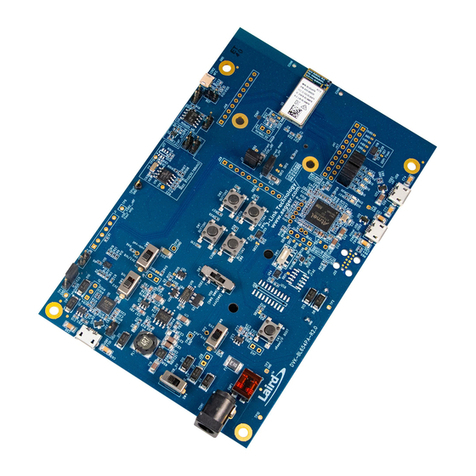
Analog Devices EVAL-ADUCM10QSPZ User manual

EVAL-ADUCM410QSPZ/EVAL-ADUCM410QSP1Z User Guide
UG-1541
One Technology Way •P. O. Box 9106 •Norwood, MA 02062-9106, U.S.A. •Tel: 781.329.4700 •Fax: 781.461.3113 •www.analog.com
ADuCM410 Development System: Getting Started Tutorial
Rev. 0 | Page 1 of 20
FEATURES
Interface through mIDAS-Link emulator
Power supply options: 9 V wall wart adapter, 5 V external
supply terminal block, or USB supply
ADuCM410 development system facilitates performance
evaluation of the ADuCM410 with a minimum of external
components
DEVELOPMENT SYSTEM KIT CONTENTS
EVAL-ADUCM410QSPZ or EVAL-ADUCM410QSP1Z evaluation
board
An Analog Devices, Inc., J-Link OB emulator (USB-SWD/
UART-EMUZ)
mIDAS-Link emulator
1 USB cable
DOCUMENTS NEEDED
ADuCM410 data sheet
ADuCM410 hardware reference manual
SOFTWARE NEEDED
ADuCM410 installer
MDIOWSD
Keil Vision5
IAR installer
IAR IDE software
GENERAL DESCRIPTION
The ADuCM410 is a fully integrated, single package device that
incorporates high performance analog peripherals together with
digital peripherals. The ADuCM410 features 16-bit, 2 MSPS data
acquisition on up to 16 input pins, an Arm® Cortex®-M33
processor, 12 voltage digital-to-analog converters (DACs), and
2 × 512 kB Flash/EE memory, packaged in a 5 mm × 5 mm, 81-ball
chip scale package ball grid array (CSP_BGA) and a 64-ball
wafer level chip scale package (WLCSP).
The ADuCM410 development system (EVAL-ADUCM410QSPZ
or EVAL-ADUCM410QSP1Z) is fully packaged to evaluate all
features of the ADuCM410, a high precision analog
microcontroller. The ADuCM410 includes 16 external AINx
channels, voltage output DACs (VDACs), four programmable
gain amplifiers (PGAs), measurement of the PGA current
channels, and various shared functions with the general-purpose
input/outputs (GPIOs) that are configurable through registers.
The VDAC channels generate an output range up to 2.5 V or
3.3 V full scale.
The EVAL-ADUCM410QSPZ and EVAL-ADUCM410QSP1Z
board uses a low noise, low dropout (LDO) linear regulator to
power up the device. The ADuCM410 is powered up using the
following three options: a 9 V wall wart adapter, a 5 V external
supply terminal block, and a USB supply.
This user guide describes how to configure the CSP_BGA
version (EVAL-ADUCM410QSPZ) and WLCSP version
(EVAL-ADUCM410QSP1Z) evaluation boards by providing
step by step procedures about the connections on the evaluation
boards. This user guide also contains information regarding
which evaluation versions of the third-party software tools to
download. Additionally, this user guide provides instructions on
how to load the supplied code examples. See Figure 1 for a
photograph of the EVAL-ADUCM410QSPZ board.
Following this guide allows users to generate and download
their own user code to use in their own unique end system
requirements.
Complete specifications for the ADucM410 are available in the
ADuCM410 data sheet, which must be consulted in conjunction
with this user guide when using the EVAL-ADUCM410QSPZ or
EVAL-ADUCM410QSP1Z board.
UG-1541 EVAL-ADUCM410QSPZ/EVAL-ADUCM410QSP1Z User Guide
Rev. 0 | Page 2 of 20
TABLE OF CONTENTS
Features .............................................................................................. 1
Development System Kit Contents ................................................ 1
Documents Needed.......................................................................... 1
Software Needed............................................................................... 1
General Description......................................................................... 1
Revision History ............................................................................... 2
EVAL-ADUCM410QSPZ Photograph........................................... 3
Evaluation Board Hardware............................................................ 4
Power Supplies and Default Link Options ................................ 4
Hardware Module............................................................................. 5
ADuCM410 and Arduino Power ............................................... 5
Arduino Connector...................................................................... 6
Getting Started .................................................................................. 7
Software Installation Procedures................................................ 7
Keil μVision5................................................................................. 7
CMSIS Pack in Keil μVision5 ......................................................8
Library and Project Options for ADuCM410 in Keil μVision5
..........................................................................................................9
IAR IDE Project Settings..............................................................9
mIDAS-Link Connector—Connecting the Hardware.......... 11
Evaluating the MDIO Download Mode.................................. 11
Evaluating the I2C Download Mode........................................ 12
Floating-Point Unit Enable Procedure .................................... 13
SRAM Mode Settings................................................................. 16
Safe Code Debugging/Development Recommendations.......... 19
Scenarios that Cause Device Lockups ..................................... 19
Recovering Locked Up Devices................................................ 19
Programmable Logic Array (PLA) Tool...................................... 20
Configuring the Gates and Output .......................................... 20
REVISION HISTORY
9/2020—Revision 0: Initial Version

UG-1541 EVAL-ADUCM410QSPZ/EVAL-ADUCM410QSP1Z User Guide
Rev. 0 | Page 4 of 20
EVALUATION BOARD HARDWARE
POWER SUPPLIES AND DEFAULT LINK OPTIONS
The EVAL-ADUCM410QSPZ or EVAL-ADUCM410QSP1Z
development system can be powered with the following options:
a 5 V terminal block from bench supplies, a 9 V wall mounted
adapter, or a USB supply. See Table 1 for the on-board jumper
configurations for each power supply option and other optional
connectors. Locate Pin 1 for each header pin for the supply.
For any of the power supply options, place the jumpers shown
in Table 1 in the required operating setup before supplying
power to the EVAL-ADUCM410QSPZ or EVAL-
ADUCM410QSP1Z (see Figure 2).
Each power supply is decoupled to the relevant ground plane
with 10 μF and 0.1 μF capacitors. Each device supply pin is also
decoupled with a 10 μF and 0.1 μF capacitor pair to the relevant
ground plane.
EVAL-ADUCM410QSPZ/EVAL-ADUCM410QSP1Z Board
Interface
The ADuCM410 has on-chip digital peripheral interfaces, such
as a universal asynchronic receiver/transmitter (UART), serial
peripheral interface (SPI), management data input/output
(MDIO), and I2C. See Figure 1 for the on-board component
locations.
Bench Power Supply Option
The ADuCM410 requires 5 V for normal operation. Replicating
the jumper configuration in Table 1, the 5 V terminal block
supply passes through LDO regulators to regulate the power
supply. The ADuCM410 can also configure the IOVDD1 and
DVDD power supplies to be 1.2 V or 1.8 V, and 1.8 V or 3.3 V,
respectively. To configure these supply options, select the
required position on Jumper P11 for IOVDD1 and Jumper P15
for DVDD. P11 and P15 are on the solder side (bottom side of
the evaluation board.)
Table 1. Jumper Configurations for the EVAL-ADUCM410QSPZ and EVAL-ADUCM410QSP1Z
Jumper No. Optional Jumper Configuration Bench Supply or 9 V Wall Wart
JP6—Future Technology Devices
International (FTDI) Supply
No Short. Yes
JP7—USB Yes Short. Yes
P11—IOVDD1 No Pin 1 and Pin 2 = 1.8 V, Pin 2 and Pin 3 = 1.2 V. Yes
P15—DVDD No Pin 1 and Pin 2 = 3.3 V, Pin 2 and Pin 3 = 1.8 V. Yes
P7—SIN1 Level Shifter Yes Pin 1 and Pin 2 = IOVDD0, Pin 2 and Pin 3 = IOVDD1. Yes
P12—SOUT1 Level Shifter Yes Pin 1 and Pin 2 = IOVDD0, Pin 2 and Pin 3 = IOVDD1. Yes
P14—LED Display Yes Short. Yes
P5—IOVDD0 Pull-Up Yes Short. Yes
JP1—SWCLK Pull-Up Yes JP3, JP4, and JP5 are optional pull-ups. The R14 resistor
(see Figure 1) must be populated with values that are at
least 100 kΩ to use these optional pull-ups.
Yes
JP2—SWDIO Pull-Up Yes Short. Yes
JP3—P2.2 or SWO Pull-Up Yes Short. Yes
JP8 to JP10 Yes These pins use the on-board FTDI chip that can be used
on the I2C downloader.
Yes
+1.2
V
P11
B
A
B
A
+5V
DGND
LDOs
P15
+1.8
V
UART
ADuCM410
IOV
DD
1
U
SB/WALL WART
MIDAS
LINK
AGND
SPI SPI
DGNDDGNDDGND
J-LINK
I
2
C
20323-006
Figure 2. On-Board Jumper Configuration Diagram

EVAL-ADUCM410QSPZ/EVAL-ADUCM410QSP1Z User Guide UG-1541
Rev. 0 | Page 5 of 20
HARDWARE MODULE
ADUCM410 AND ARDUINO POWER
Customers may want to connect their own custom circuits to
the EVAL-ADUCM410QSPZ or EVAL-ADUCM410QSP1Z
evaluation board.
Four connectors of the EVAL-ADUCM410QSPZ and EVAL-
ADUCM410QSP1Z evaluation boards support an Arduino®
Uno or Arduino Zero connection interface to external PCBs.
The EVAL-ADUCM410QSPZ/EVAL-ADUCM410QSP1Z
evaluation boards can power the external Arduino-based board.
Inversely, the Arduino is also capable of powering up the whole
module, including the ADuCM410. Table 2 shows the jumper
connections for the power configurations of the EVAL-
ADUCM410QSPZ/EVAL-ADUCM410QSP1Z and the
Arduino.
Table 2. Power Configurations for the EVAL-ADUCM410QSPZ (BGA) and EVAL-ADUCM410QSP1Z (WLCSP)
EVAL-ADUCM410QSPZ EVAL-ADUCM410QSP1Z Optional Jumper Information Jumper Configuration
P22 P20 Yes
Power selection either via
USB power or via Arduino
power
Pin 1 and Pin 2 = USB powered. Pin 2 and
Pin 3 = Arduino powered. Do not use USB
power for the EVAL-ADUCM410QSPZ or
EVAL-ADUCM410QSP1Z board if the
Arduino and the evaluation board are
powered up together.
JP16 JP16 Yes Power from Arduino via
the EVAL-ADUCM410QSPZ
or EVAL-ADUCM410QSP1Z
board
If this jumper is shorted, the
EVAL-ADUCM410QSPZ or
EVAL-ADUCM410QSP1Z also power up
the Arduino.
JP111JP111Yes 3.3 V LDO output Short.
JP121JP121Yes
3.3 V power to Arduino
IOREF pin
Short.
JP131JP131Yes
ADuCM410 reset to
Arduino reset
Short.
JP141JP141Yes 3.3 V power to Arduino Short.
JP151JP151Yes 5 V power to Arduino Short.
1The JP11 to JP15 connectors are used if the Arduino is powered up via the EVAL-ADUCM410QSPZ or EVAL-ADUCM410QSP1Z board.

UG-1541 EVAL-ADUCM410QSPZ/EVAL-ADUCM410QSP1Z User Guide
Rev. 0 | Page 6 of 20
ARDUINO CONNECTOR
The EVAL-ADUCM410QSPZ and EVAL-ADUCM410QSP1Z
have Arduino R3 headers directly compatible with Arduino
Uno and Arduino Zero. Using the EVAL-ADUCM410QSPZ
or EVAL-ADUCM410QSP1Z board with Arduino Uno or
equivalent is recommended. The Arduino pins used by the
EVAL-ADUCM410QSPZ or EVAL-ADUCM410QSP1Z board
are given in Table 3.
For more information on the ADuCM410 pins, refer to the
ADuCM410 data sheet and ADuCM410 hardware reference
manual (UG-1807).
Table 3. EVAL-ADUCM410QSPZ/EVAL-
ADUCM410QSP1Z Pin Connections to Arduino Pins
EVAL-ADUCM410QSPZ (CSP_BGA)/
EVAL-ADUCM410QSP1Z (WLCSP)
R3 Header Pins Arduino Pin
Digital
P13 (Both EVAL-ADUCM410QSPZ and EVAL-
ADUCM410QSP1Z)
P1.2/SCL1 SCL
P1.3/SDA1 SDA
AREF AREF
DGND GND
P0.0/SCLK0 SCK
P0.1/MISO0 MISO
P0.2/MOSI0 MOSI
P2.0 SS
P0.3/CS0 GPIO
P2.1/IRQ2 GPIO
P18 (EVAL-ADUCM410QSPZ) and
P16 (EVAL-ADUCM410QSP1Z)
P1.0/SIN1 RXD
P1.1/SOUT1 TXD
P0.6/SCL2 GPIO
P0.7/SDA2 GPIO
P1.4/SCLK1 GPIO
P1.5/MISO1 GPIO
P1.6/MOSI1 GPIO
P1.7/CS1 GPIO
EVAL-ADUCM410QSPZ (CSP_BGA)/
EVAL-ADUCM410QSP1Z (WLCSP)
R3 Header Pins Arduino Pin
P19 (EVAL-ADUCM410QSPZ) and
P18 (EVAL-ADUCM410QSP1Z)
P0.1/MISO0 MISO
IOVDD0 3.3V
P0.0/SCLK0 SCK
P0.2/MOSI0 MOSI
RESET RESET
DGND GND
Power
P20 (EVAL-ADUCM410QSPZ) and
P19 (EVAL-ADUCM410QSP1Z)
Arduino or ADuCM410 Power 7V VIN
AGND GND
AGND GND
Arduino or ADuCM410 Power 5V
Arduino or ADuCM410 Power 3V3
Arduino or ADuCM410 Reset RESET
Arduino or ADuCM410 Power IOREF
No Connect No connect
Analog
P21 (Both EVAL-ADUCM410QSPZ and EVAL-
ADUCM410QSP1Z)
AIN0 ADC5
AIN1 ADC4
AIN2 ADC3
AIN3 ADC2
AIN4 ADC1
AIN14 ADC0

EVAL-ADUCM410QSPZ/EVAL-ADUCM410QSP1Z User Guide UG-1541
Rev. 0 | Page 7 of 20
GETTING STARTED
SOFTWARE INSTALLATION PROCEDURES
Perform the following steps before plugging any of the USB
devices into the PC:
1. Close all open applications on the PC.
2. After downloading the ADuCM410 installer from
ftp://ftp.analog.com/pub/microconverter/ADucM410, double
click ADuCM410Installer-V0.1.0.0.exe and follow the
instructions shown in Figure 3. The ADuCM410-Installer
Setup window displays the installation method and
component selection as shown in Figure 3. The end user
license agreement (EULA) is displayed after proceeding
through the ADuCM410Installer Setup window. Accepting
the EULA extracts the installer, and rejecting the EULA
cancels the installer.
20323-002
Figure 3. Installation Options
3. After installation, the \AnalogDevices\ADuCM410 folder
opens. This location contains the examples folder that stores
the example codes for the ADuCM410 (see Figure 4).
20323-003
Figure 4. ADuCM410 examples Folder with Projects
KEIL µVISION5
The Keil μVision5® integrated development environment (IDE)
integrates all the tools necessary to edit, assemble, and debug
code. The fastest way to begin running the Keil IDE is to open
an existing project by using the following steps:
1. In Keil, click Project > Open Project.
2. Browse to the folder where the ADuCM410 software is
installed (C:\AnalogDevices\ADuCM410...).
3. Open the M410_GPIO.uvprojx file, located in the
ADuCM410\examples\M410_GPIO\ARM folder.
Opening the file launches an example project.
4. Set up the Cortex microcontroller software interface
standard (CMSIS) pack before proceeding through the
source. See the CMSIS Pack in Keil μVision5 section for
details on how to import the CMSIS pack.
5. Compile and download the source code to the EVAL-
ADUCM410QSPZ or EVAL-ADUCM410QSP1Z board
through the menu bar on the IDE.
6. To run the source code, press RESET on the EVAL-
ADUCM410QSPZ or EVAL-ADUCM410QSP1Z board
and then press RUN.
7. When running the code, the green LED on the board
marked DISPLAY flashes.

UG-1541 EVAL-ADUCM410QSPZ/EVAL-ADUCM410QSP1Z User Guide
Rev. 0 | Page 8 of 20
CMSIS PACK IN KEIL µVISION5
After the Keil μVision5® IDE is installed, open the application
and use the following steps to properly set up the ADuCM410
device from the IDE:
1. Open the CMSIS pack installer as shown in Figure 5.
When the pack installer is opened for the first time, it may
take a few minutes to update the pack installer.
20323-105
Figure 5. Pack Installer
2. After the CMSIS pack installer has opened, click File >
Import. Select and import the ADuCM410 pack that is
included in the installation setup (see Figure 6).
3. With the ADuCM410 CMSIS pack installed, the
ADuCM410 device is supported by the Keil μVision5 IDE.
The ADuCM410 appears in the Device tab of the Keil
window, as shown in Figure 7.
20323-106
Figure 6. Pack Installer
20323-107
Figure 7. ADuCM410 Device in Keil μVision5

EVAL-ADUCM410QSPZ/EVAL-ADUCM410QSP1Z User Guide UG-1541
Rev. 0 | Page 9 of 20
LIBRARY AND PROJECT OPTIONS FOR ADUCM410
IN KEIL µVISION5
The Keil μVision5 project files are placed in the Arm folder for
each example program. For example, C:\Analog Devices\
ADuCM410\examples\M410_Adc\ARM\M410_Adc.uvporjx
is the file that is opened by Keil. By clicking the Manage Run-
Time Environment icon from the Keil settings menu (see
Figure 8), users can select the components needed from
Peripheral Libraries in their project, as shown in Figure 10.
20323-108
Figure 8. Manage Run-Time Environment Icon
IAR IDE PROJECT SETTINGS
It is recommended for first time users to open an example
project from the examples folder. For instance, the
M410_Adc.eww file is the IAR Embedded Workbench® project
file for the ADC example, and it can be opened from the
C:\Analog Devices\ ADuCM410\examples\M410_Adc\IAR\
folder.
Opening an example file allows compilation, programming, and
debugging without any configuration changes from the user.
If creating a new IAR-based project, the following steps must be
completed to run the ADuCM410 example programs properly:
1. From the Project menu, select Options.
2. Click the General Options category, and ensure the
selected device is Analog Devices ADuCM410 under the
Target tab.
20323-110
Figure 9. IAR Project Setting
20323-109
Figure 10. Peripheral Libraries

UG-1541 EVAL-ADUCM410QSPZ/EVAL-ADUCM410QSP1Z User Guide
Rev. 0 | Page 10 of 20
3. After the ADuCM410 device is selected, click the Library
Configuration tab. Ensure that all settings match those
shown in Figure 11.
20323-111
Figure 11. IAR Library Configuration
4. Next, click C/C++ Compiler, and check that the
directories match those shown in the Additional include
directories box (see Figure 12).
20323-112
Figure 12. C/C++ Compiler Setting
5. Next, click the Linker category, check the Override default
box in the Config tab, and browse for the linker file under
the Linker configuration file section, as shown in
Figure 13.
20323-113
Figure 13. Linker Setting
6. Check the Debugger settings and ensure that all settings
match those shown in Figure 14 and Figure 15 in the
Download and Setup tabs.
20323-114
Figure 14. Debugger Configuration

EVAL-ADUCM410QSPZ/EVAL-ADUCM410QSP1Z User Guide UG-1541
Rev. 0 | Page 11 of 20
20323-115
Figure 15. J-Link/J-Trace Selected in Setup Tab
5. Check that the J-Link/J-Trace settings in the Setup tab
match those as shown in Figure 16.
2
0323-116
Figure 16. J-Link/J-Trace Settings
6. Click OK, and the user can start configuring the example
program for the ADuCM410 in the IAR IDE.
mIDAS-LINK CONNECTOR—CONNECTING THE
HARDWARE
Use the following steps to connect the mIDAS-Link to the
EVAL-ADUCM410QSPZ or EVAL-ADUCM410QSP1Z:
1. Connect the provided USB cable between the PC and the
mIDAS-Link connector.
2. The yellow LED lights up on the mIDAS-Link to indicate
the connection to the EVAL-ADUCM410QSPZ or EVAL-
ADUCM410QSP1Z is initializing.
3. Install the driver for the ADuCM410. Driver installation
details are included in a .exe file in the ADuCM410
installer.
After connecting the mIDAS-link hardware to the EVAL-
ADUCM410QSPZ or EVAL-ADUCM410QSP1Z, the mIDAS-
Link can be used in Keil μVision5 and IAR Embedded
Workb ench d e velopment.
Table 4 shows the mIDAS-Link pin configuration.
Table 4. mIDAS-Link Pin Labels
EVAL-ADUCM410QSPZ/EVAL-
ADUCM410QSP1Z Header Pin No.
mIDAS-Link Pin
Labels
1, 2 DVDD
3, 11, 19 NC
4, 6, 8,10, 12, 14, 16, 18 DGND
5 P1.0/SIN0
7 SWDIO
9 SWCLK
13 P2.2/SWO
option via JP4
15 RESET
17 P1.1/SOUT
EVALUATING THE MDIO DOWNLOAD MODE
The MDIO downloader can be extracted from the installer on
the ftp://ftp.analog.com/pub/microconverter/ADucM410
website. Use the MDIO downloader with the MDIOWSD
software to download the hexadecimal files. Use the SUB-20
multiple interface USB adapter (not included) to connect the
EVAL-ADUCM410QSPZ or EVAL-ADUCM410QSP1Z to the
PC via the MDIOWSD software tool. The Windows 10
Operating System section outlines the procedure to download
code and the example programs from the installer to the
ADuCM410 device using the MDIO interface.
Windows 10 Operating System
After connecting the SUB-20 multiple interface USB adapter to
the PC, the USB adapter automatically installs the needed SUB-20
software. To ensure the software properly installs and connects
to the EVAL-ADUCM410QSPZ or EVAL-ADUCM410QSP1Z,
follow these steps:
1. Double click the SUB-20 firmware updater.exe file
installed on the PC after the SUB-20 adapter is connected
to open the graphical user interface (GUI) shown in Figure 17.

UG-1541 EVAL-ADUCM410QSPZ/EVAL-ADUCM410QSP1Z User Guide
Rev. 0 | Page 12 of 20
20323-008
Figure 17. GUI for Updating the SUB-20 Firmware
2. For Windows® 10, Figure 17 may open automatically to
update the SUB-20 adapter without having to double click
the SUB-20 firmware updater.exe file. Click the Update
button. For Windows 7 and earlier versions, users may not
need to update the SUB-20 adapter.
3. After the adapter finishes updating, connect the pins on the
SUB-20 board to the pins on the EVAL-ADUCM410QSPZ
or EVAL-ADUCM410QSP1Z as described in Table 5.
4. On the SUB-20 board, ensure that Pin J7 is set to 3.3 V,
Pin JP1 to Pin JP4 and Pin JP5 are set to connect Header
Pin 1 to Header Pin 2, and Pin JP6 is set to connect Header
Pin 2 to Header Pin 3.
5. Connect the USB cable from the PC to the SUB-20 board and
run C:\ADuCM410…\SoftwareTools\MDIOWSD\
MDIOWSD.exe. The GUI window then opens, as shown
in Figure 18.
6. Click the Browse button (see Figure 18), and navigate to
the desired code to download.
20323-009
Figure 18. MDIOWSD GUI
4. To download the code, select Program and Verify from
the Flash Action box, click Start, and follow the
instructions listed on the GUI.
Table 5. SUB-20 to EVAL-ADUCM410QSPZ/
EVAL-ADUCM410QSP1Z Pin Connection Guide
EVAL-ADUCM410QSPZ/ EVAL-
ADUCM410QSP1Z Pins on P3 SUB-20 Pins
DGND J6-10
1.2V J6-9
MDIO J6-7
MCK J6-1
For more information about flash block switching and the
MDIO, refer to the ADuCM410 hardware reference manual
(UG-1807).
EVALUATING THE I2C DOWNLOAD MODE
The I2C downloader can be extracted from the installer on the
ftp://ftp.analog.com/pub/microconverter/ADucM410 website. Use
the I2C downloader with the M12CFTWSD software to
download the hexadecimal files. Use the on-board FTDI chip to
interface with the device. The FTDI chip allows connectivity
between the EVAL-ADUCM410QSPZ or EVAL-
ADUCM410QSP1Z board and the PC via the MI2CFTWSD
software tool. When the downloader is extracted, follow these
steps:
1. On the EVAL-ADUCM410QSPZ or EVAL-
ADUCM410QSP1Z, ensure JP7, JP8, JP9, and JP10 are
shorted to use the on-board FTDI chip.
2. Open the MI2CFTWSD folder, and double click
MI2CFTWSD.exe.
3. The GUI opens, as shown in Figure 19.
2
0323-117
Figure 19. MI2CFTWSD GUI

EVAL-ADUCM410QSPZ/EVAL-ADUCM410QSP1Z User Guide UG-1541
Rev. 0 | Page 13 of 20
4. Settings such as Mass Erase and Program can be found by
clicking Configure, then the Flash tab. Select Mass Erase
or Program as needed, and click OK.
20323-118
Figure 20. Mass Erase and Program Options in MI2CFTWSD
5. On the EVAL-ADUCM410QSPZ or EVAL-
ADUCM410QSP1Z board, press the
SERIAL_DOWNLOAD button and pulse the RESET
button to set up the device in I2C download mode.
6. Click the Start button in the MI2CFTWSD window. If the
I2C connection is established, the status shows the
ADuCM410 is connected, as shown in Figure 21.
20323-119
Figure 21. I2C Connection Established
7. After I2C connection is established. Click the Run button
and it automatically flashes the device and either mass
erases or downloads the program, depending on the
configuration that the user selected in Step 4. Figure 22
shows an example of a complete mass erase on the device.
2
0323-120
Figure 22. Complete Mass Erase
8. Repeat Step 4 through Step 7 to select another option from
the software tool.
FLOATING-POINT UNIT ENABLE PROCEDURE
The settings shown in the Project dropdown menu (see Figure 23)
are available on the Keil and IAR software tool environment. By
default, the floating-point unit (FPU) is disabled after the
settings are disabled. Code to enable and output the floating-
point value is added in the SystemInit function in the
system_ADuCM410.c file. This file is located in the example
program in the ADuCM410 installer folder named M410_FPU
(under the Files list in Figure 23).
Running the IAR FPU Program
Perform the following steps before running the FPU example
program in the IAR IDE software (downloaded from the
provided IAR installer).
1. After opening the IAR IDE, click the Project dropdown
menu and select Options (see Figure 23).
20323-010
Figure 23. Selecting Options in the IAR IDE
2. From the Category section, click General Options. Then
click the Target tab, and ensure the FPU box in the
Floating point settings section is set to VFPv5 single
precision, as shown in Figure 24.
20323-011
Figure 24. IAR IDE General Options

UG-1541 EVAL-ADUCM410QSPZ/EVAL-ADUCM410QSP1Z User Guide
Rev. 0 | Page 14 of 20
3. After setting the Floating point settings options, run the
FPU example program. Running the debug mode causes
the Output section in the Term i nal I/O window to display
fractional values of the variables, as shown in Figure 26.
Running the Keil FPU Program
Perform the following steps before running the FPU example
program from the Keil IDE (included on the ADuCM410
installer).
1. After opening the Keil IDE, click the Flash dropdown
menu and select the Configure Flash Tools option (see
Figure 25).
20323-013
Figure 25. Keil Flash Dropdown Menu Options
2. Selecting the Configure Flash Tools option opens the
window shown in Figure 28. Click the Target tab, and
ensure the Floating Point Hardware dropdown box is set
to the Single Precision option, as shown in Figure 28.
20323-012
Figure 26. IAR FPU Example Program Output
20323-014
Figure 27. Keil General Options

EVAL-ADUCM410QSPZ/EVAL-ADUCM410QSP1Z User Guide UG-1541
Rev. 0 | Page 15 of 20
3. After establishing the settings shown in Figure 28, run the
FPU example code from the C:\Analog Devices\
ADuCM410\examples\M410_FPU folder in the example
code folder. In debug mode, the output Disassembly
window displays fractional values of the variables, as
shown in Figure 29.
20323-014
Figure 28. Keil General Options
20323-015
Figure 29. Keil FPU Example Program Output

UG-1541 EVAL-ADUCM410QSPZ/EVAL-ADUCM410QSP1Z User Guide
Rev. 0 | Page 16 of 20
SRAM MODE SETTINGS
Configuration settings are available on the Keil and IAR
software tool environments. To properly set up and test the
static random access memory (SRAM) modes, go to the
example projects located in the M410_SramMode installer.
IAR SRAM Mode
Three file settings must be completed to configure the
corresponding SRAM mode: main.c, startup_ADuCM410.s,
and ADuCM410flash_SramMode.icf.
1. After the example program is opened from the IAR IDE,
ensure that the macros shown in Figure 30 are set up and
commented in to select the SRAM mode the linker file is
operating in. The M410_SramMode example code (see
Figure 31) uses a linker file, the ADuCM410flash_
SramMode.icf file (see Figure 32) placed in the IAR folder
within the SramMode example program.
20323-016
Figure 30. IAR SRAM Setup main.c
5. Configure the macros shown in Figure 30, Figure 31, and
Figure 32 to run the SRAM modes. Ensure the main.c,
startup_ADuCM410.s, and
ADuCM410flash_SramMode.icf macros are selected with
the correct SRAM mode.
6. Users can select the desired USER_SRAM_MODE macro
as shown in Figure 31 and Figure 32. Users can also select
the TEST_SRAM_MODE macro as shown in Figure 30.
By default, the example program is running in TEST_SRAM_
MODE 0. Ensure the main.c macro, which runs the debug
mode, shows that the instruction SRAM (ISRAM) is placed
in debug mode. If the ISRAM is in debug mode, the
Disassembly window from the View menu bar displays the
isramTestFunc with the 0x10000000 address (see Figure 33).
20323-017
Figure 31. IAR SRAM Setup startup_ADuCM410.s SRAM Modes
20323-018
Figure 32. IAR SRAM Setup ADuCM410flash_SramMode.icf Macros
20323-019
Figure 33. IAR SRAM Output at Mode 0

EVAL-ADUCM410QSPZ/EVAL-ADUCM410QSP1Z User Guide UG-1541
Rev. 0 | Page 17 of 20
Keil SRAM Mode
Several .sct and .s files from the example program allow users to
select the desired SRAM: M410_SramModeX.sct and
SetSramModeX.s. The X in the file name specifies mode
number (0 to 3) for the SRAM.
1. After the example program is opened from the Keil IDE, the
files located in the same folder are shown. Ensure that the
.sct and .s files from the example folder (see Figure 34) are
used with the corresponding SRAM mode being tested.
20323-020
Figure 34. SRAM Mode .sct and .s Files
7. By default, the M410_SramMode macro uses SRAM
Mode 0. The SetSramMode0.s assembly file is added to
the subdirectory shown in Figure 35. Specify which SRAM
mode to test in the main.c file. By default, SRAM Mode 0 is
tested (see Figure 36).
20323-021
Figure 35. Set Up SetSramMode0.s
20323-022
Figure 36. Set Up M410_SramMode0.sct
8. After following Step 1 and Step 2, proceed to set up the .sct
file located in Flash > Configure Flash Tools > Linker. Refer
to Figure 37 to check the settings circled in green are
correct and that the correct scatter file is chosen (based on
the SRAM mode configuration).
9. Running the settings in Figure 38 shows that the ISRAM is
placed in debug mode via the Disassembly window.

EVAL-ADUCM410QSPZ/EVAL-ADUCM410QSP1Z User Guide UG-1541
Rev. 0 | Page 19 of 20
SAFE CODE DEBUGGING/DEVELOPMENT RECOMMENDATIONS
The ADuCM410 code development and programming tools are
similar or identical to those used on other Analog Devices
microcontroller devices and to microcontrollers from other
companies. Care must be taken to ensure the device can be
reprogrammed to avoid lockup situations. In a lockup, the
connection to the ADuCM410 via programming/debug tools is
no longer possible.
This section lists scenarios that can cause lockup situations. If a
lockup situation occurs, recommendations are provided to
recover a device.
SCENARIOS THAT CAUSE DEVICE LOCKUPS
Page 0 Checksum Error
Address 0x1FFC contains a 32-bit checksum for Flash Page 0.
The on-chip kernel performs a checksum on Page 0 excluding
0x1FFC to 0x1FFF. If the kernel result does not match the value
at 0x1FFC or if 0x1FFC value is not 0xFFFFFFFF, the kernel
detects corruption of Page 0 and does not exit to user code,
resulting in a device lockup. See the ADuCM410 hardware
reference manual (UG-1807) for information about an integrity
check of the internal Flash Page 0 by the on-chip kernel.
To recover from this situation, mass erase the device via the
downloader tool (I2C or MDIO), and ensure the user source
code sets Flash Address 0x01FFC = 0xFFFFFFFF.
The example code for the ADuCM410 configures Flash Address
0x01FFC = 0xFFFFFFFF.
See page0_checksum in the system_ADuCM410.c file.
User Flash Pages—Corruption of Reserved Locations
The top six 32-bit locations of each flash block are reserved, and
care must be taken not to overwrite these locations. The flash
signature for each block and the write protection settings are
stored in these six locations. See the ADuCM410 Hardware
Reference Manual for information about flash user space
organization.
Ensure the top 32-bit location in each flash page is reserved.
See the example programs included in the installer for details.
Unexpected Resets
Unexpected watchdog resets, software resets, power-on resets,
or external resets can cause debug/programming sessions to
end abruptly because these resets break the SWD interface
between the J-Link and the Cortex core.
If the user source code results in regular resets, try mass erasing
the user flash via the downloader and restart the debug session.
Power Saving Modes
If the user code puts the Cortex core into a power-down state,
the power-down causes issues after a power cycle for the debug
tools that use the SWD interface. Tools like J-Link require the
Cortex core to be fully active.
Keil CMSIS Pack
For Keil μVision users only, ensure Keil CMSIS pack
Version 1.4.0 or later is being used.
RECOVERING LOCKED UP DEVICES
Mass erase the device via either the MDIO or I2C downloader
tool.

UG-1541 EVAL-ADUCM410QSPZ/EVAL-ADUCM410QSP1Z User Guide
Rev. 0 | Page 20 of 20
PROGRAMMABLE LOGIC ARRAY (PLA) TOOL
The ADuCM410 integrates a PLA that consists of two
independent but interconnected PLA blocks. Each block
consists of 16 elements, giving a total of 32 elements listed from
Element 0 to Element 31. The PLA tool is a graphical tool that
allows easy configuration of the PLA. The PLA tool can be
found on the ADuCM410 installer, under the Tools folder. With
the PLA tool, the correct output value is determined after all the
options from the tool is properly selected.
CONFIGURING THE GATES AND OUTPUT
PLA elements contains a two-input lookup table that can be
configured to generate logic output function based on the two
inputs and flip flop in the PLA, as shown in Figure 39. Each
PLA element in a block can be connected to other elements in
the same block by configuring the output of Mux 0 and Mux 1.
The user can select respective inputs that correspond to the
PLA_ELEMx register bits. See the ADuCM410 Hardware
Reference Manual for a complete list of possible connections for
the element GPIO input/output, and for the lookup table
configuration in the PLA.
After the inputs are selected from the GUI, ensure that the
BLOCK, ELEMENT, and LOOK UP TABLE options are
selected in the top right portion of the tool. Click the ENTER
button to generate the output of PLA (see Figure 39).
20323-121
Figure 39. Programmable Logic Array Tool
I2C refers to a communications protocol originally developed by Philips Semiconductors (now NXP Semiconductors).
ESD Caution
ESD (electrostatic discharge) sensitive device. Charged devices and circuit boards can discharge without detection. Although this product features patented or proprietary protection
circuitry, damage may occur on devices subjected to high energy ESD. Therefore, proper ESD precautions should be taken to avoid performance degradation or loss of functionality.
Legal Terms and Conditions
By using the evaluation board discussed herein (together with any tools, components documentation or support materials, the “Evaluation Board”), you are agreeing to be bound by the terms and conditions
set forth below (“Agreement”) unless you have purchased the Evaluation Board, in which case the Analog Devices StandardTerms and Conditions of Sale shall govern. Do not use the Evaluation Board until you
have read and agreed to the Agreement. Your use of the Evaluation Board shall signify your acceptance of the Agreement. This Agreement is made by and between you (“Customer”) and Analog Devices, Inc.
(“ADI”), with its principal place of business at One Technology Way, Norwood, MA 02062, USA. Subject to the terms and conditions of the Agreement, ADI hereby grants to Customer a free, limited, personal,
temporary, non-exclusive, non-sublicensable, non-transferable license to use the Evaluation Board FOR EVALUATION PURPOSES ONLY. Customer understands and agrees that the Evaluation Board is provided
for the sole and exclusive purpose referenced above, and agrees not to use the Evaluation Board for any other purpose. Furthermore, the license granted is expressly made subject to the following additional
limitations: Customer shall not (i) rent, lease, display, sell, transfer, assign, sublicense, or distribute the Evaluation Board; and (ii) permit anyThird Party to access the Evaluation Board. As used herein, the term
“Third Party” includes any entity other than ADI, Customer, their employees, affiliates and in-house consultants. The Evaluation Board is NOT sold to Customer; all rights not expressly granted herein, including
ownership of the Evaluation Board, are reserved by ADI. CONFIDENTIALITY. This Agreement and the Evaluation Board shall all be considered the confidential and proprietary information of ADI. Customer may
not disclose or transfer any portion of the Evaluation Board to any other party for any reason. Upon discontinuation of use of the Evaluation Board or termination of this Agreement, Customer agrees to
promptly return the Evaluation Board to ADI. ADDITIONAL RESTRICTIONS. Customer may not disassemble, decompile or reverse engineer chips on the Evaluation Board. Customer shall inform ADI of any
occurred damages or any modifications or alterations it makes to the Evaluation Board, including but not limited to soldering or any other activity that affects the material content of the Evaluation Board.
Modifications to the Evaluation Board must comply with applicable law, including but not limited to the RoHS Directive. TERMINATION. ADI may terminate this Agreement at any time upon giving written
notice to Customer. Customer agrees to return to ADI the Evaluation Board at that time. LIMITATION OF LIABILITY. THE EVALUATION BOARD PROVIDED HEREUNDER IS PROVIDED “AS IS” AND ADI MAKES NO
WARRANTIES OR REPRESENTATIONS OF ANY KIND WITH RESPECT TO IT. ADI SPECIFICALLY DISCLAIMS ANY REPRESENTATIONS, ENDORSEMENTS, GUARANTEES, OR WARRANTIES, EXPRESS OR IMPLIED,
RELATED TO THE EVALUATION BOARD INCLUDING, BUT NOT LIMITED TO, THE IMPLIED WARRANTY OF MERCHANTABILITY, TITLE, FITNESS FOR A PARTICULAR PURPOSE OR NONINFRINGEMENT OF
INTELLECTUAL PROPERTY RIGHTS. IN NO EVENT WILL ADI AND ITS LICENSORS BE LIABLE FOR ANY INCIDENTAL, SPECIAL, INDIRECT, OR CONSEQUENTIAL DAMAGES RESULTING FROM CUSTOMER’S
POSSESSION OR USE OF THE EVALUATION BOARD, INCLUDING BUT NOT LIMITED TO LOST PROFITS, DELAY COSTS, LABOR COSTS OR LOSS OF GOODWILL. ADI’S TOTAL LIABILITY FROM ANY AND ALL CAUSES
SHALL BE LIMITED TO THE AMOUNT OF ONE HUNDRED US DOLLARS ($100.00). EXPORT. Customer agrees that it will not directly or indirectly export the Evaluation Board to another country, and that it will
comply with all applicable United States federal laws and regulations relating to exports. GOVERNING LAW. This Agreement shall be governed by and construed in accordance with the substantive laws of the
Commonwealth of Massachusetts (excluding conflict of law rules). Any legal action regarding this Agreement will be heard in the state or federal courts having jurisdiction in Suffolk County, Massachusetts, and
Customer hereby submits to the personal jurisdiction and venue of such courts. The United Nations Convention on Contracts for the International Sale of Goods shall not apply to this Agreement and is
expressly disclaimed.
©2020 Analog Devices, Inc. All rights reserved. Trademarks and
registered trademarks are the property of their respective owners.
UG20323-9/20(0)
This manual suits for next models
1
Table of contents
Other Analog Devices Microcontroller manuals

Analog Devices
Analog Devices EV1HMC8362LP6G User manual

Analog Devices
Analog Devices DC1840C Quick setup guide

Analog Devices
Analog Devices ADRV9001 User manual

Analog Devices
Analog Devices AN-951 Installation and operating instructions

Analog Devices
Analog Devices ADuCM4050 EZ-KIT User manual

Analog Devices
Analog Devices Linear Technology ADI Power DC3159A Quick setup guide

Analog Devices
Analog Devices EV-AD7284TMSDZ User manual

Analog Devices
Analog Devices MicroConverter ADuC706x Specification sheet

Analog Devices
Analog Devices ADuCM360 User manual

Analog Devices
Analog Devices ADuCM355 Quick user guide