Evaluation Board User Guide UG-
Rev. Pr C | Page 3 of 17
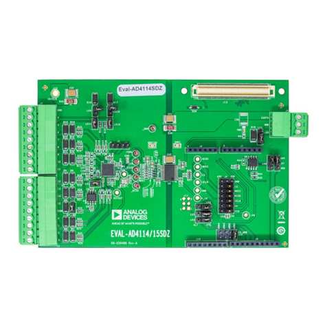
EVALUATION BOARD HARDWARE
OVERVIEW
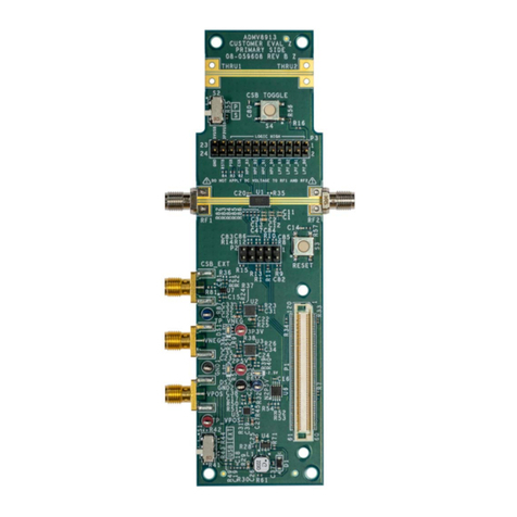
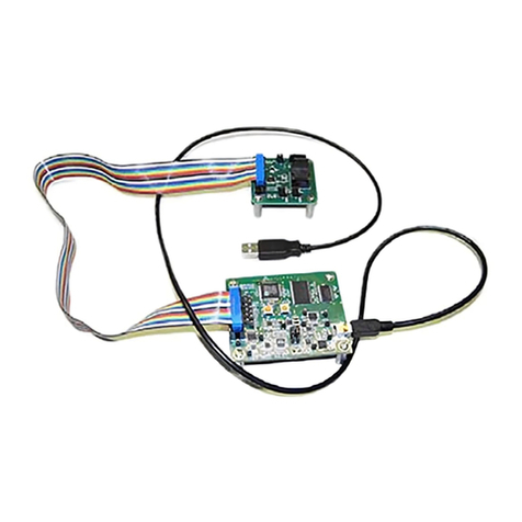
The EV-ADF5355SD1Z requires the SPD-S platform which
uses the EVAL-SDP-CS1Z. (SDP-B is not recommended).
POWER SUPPLIES
The EV-ADF5355SD1Zis powered from dc power connectors
(4 mm banana connectors). When feeding via banana
connectors, 6.0 V is a suitable feeding voltage. The power
supply circuitry allows the user to use two or three separate
LDOs to feed the ADF5355 (using fewer LDOs increases the
risk of spur contaminated dc feeds). Ensure the switch is in the
correct position to power the board. Consult the board
schematic in Figure 20, Figure 21, and Figure 22 to determine a
suitable setting.
The charge pump and VCO supply pins are driven from a 5V
ADM7150 high performance low noise regulator. The
remaining supplies are powered from 3.3V ADM7150’s.
An LED, indicates when USB power is available, and another
LED, indicates when the ADF5355 is powered on. Switch S1 is
used to power the ADF5355 from the external dc connectors,
and should be switched to the left.
In case the SDP processor causes spurs on the RF output signal,
the user may remove this connector and measure the spurious.
RF OUTPUT
The EV-ADF5355SD1Z has one pair of SMA output connectors
(differential outputs RFoutA+/-). The device is quite sensitive to
impedance unbalance. If only one port of a differential pair is
used, terminate the other with a 50 Ω load. If only RFoutB is
used, then it can be powered off, or if left on, both RFoutA pins
should be terminated in 50 Ohms.
The RFoutB contains the high frequency (6.8 – 13.6 GHz) and
is a single ended RF output.
LOOP FILTER
The loop filter schematic is included in the board schematic on
Figure 20. The loop filter component placements are clarified in
Figure 2. Customers wishing for lowest noise at 100 kHz offset
are advised to use the following components, and to use 0.9 mA
charge pump current, which are inserted on the evaluation
board.
C60 = 22 nF, C59 = 0.47 uF, C14 = 10 nF, C73 = 10 pF.
R14 = 220 Ohms, R1 = 470 Ohms.
Customers wishing for lowest rms phase noise should use:
C60 = 1.2 nF, C59 = 33 nF, C14 = 390 pF, C73 = 10 pF.
R14 = 1 kOhms, R17 = 3.3 kOhm.
And also program the 0.9 mA charge pump current.
Figure 2. Loop Filter Placement
REFERENCE SOURCE
The evaluation board contains a footprint for a 122.88 MHz
differential output TCXO from Vectron. If preferred, the user
may supply either a single-ended or differential reference input
to connectors REFINA and REFINB. Disconnect the power rail
to the TCXO by removing resistor R12 first.
To use a single ended REFIN, then connect a low noise 122.88
MHz reference source to REFINB. To use a differential REFIN
connect the differential signal to REFINA and REFINB. The
differential REFIN can operate to 500 MHz input frequency.
If the TCXO is removed, then an external REFIN must be used.
