Blu STUDIO 5.0 S User manual

1
BLU Studio 5.0S
Service Manual

1
Table of Contents
INTRODUCTION........................................................................................................................................................................4
1 .HARDWARE SYSTEM INTRODUCTION..................................................................................................................................5
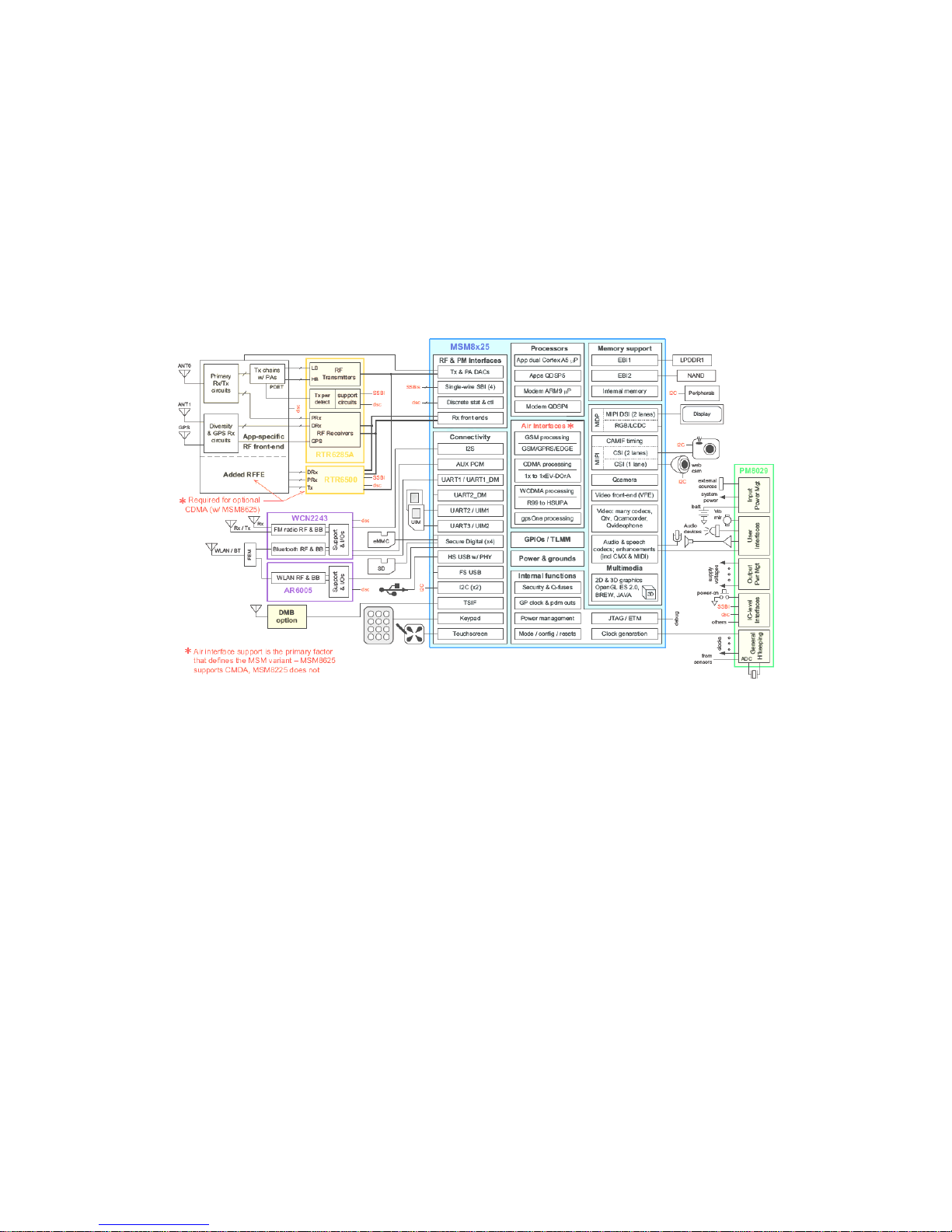
1.1 The framework of the hardware system .......................................................................................................................5
1.2 Studio 5.0S Main Components ......................................................................................................................................6
2. The detail of system’s modules ...........................................................................................................................................9
2.1 RF module ......................................................................................................................................................................9
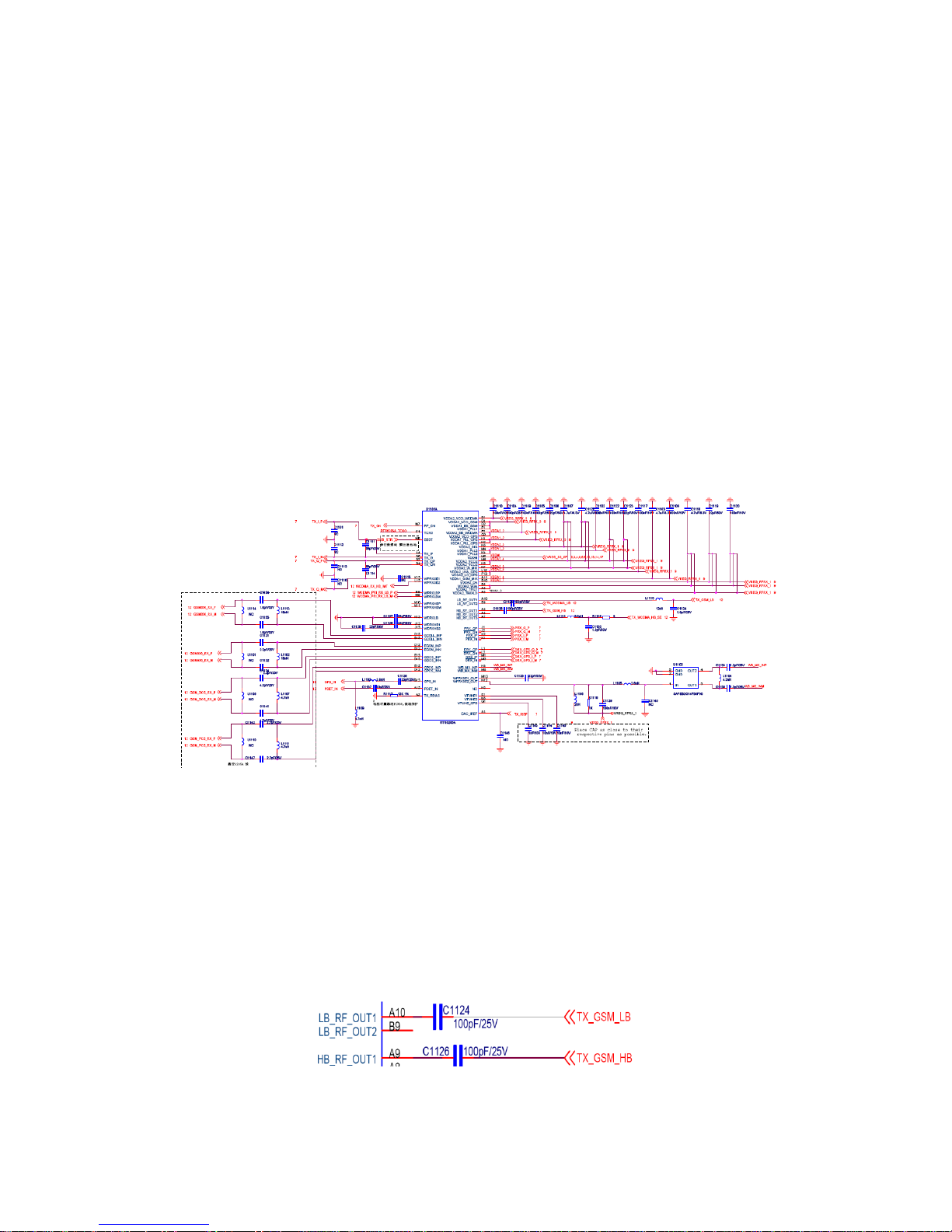
2.1.1 Transceiver..............................................................................................................................................................9
2.1.2 GSM signal’s path....................................................................................................................................................9
2.1.3 WCDMA signal’s path ...........................................................................................................................................11
2.2 PMU .............................................................................................................................................................................14
2.2.1 The timing of system’s boot..................................................................................................................................14
2.2.2 The voltages put out from PMU ...........................................................................................................................14
2.3 Memory .......................................................................................................................................................................15
2.4 Audio module...............................................................................................................................................................16
2.4.1 Microphone circuit................................................................................................................................................16
2.4.2 Earpiece circuit......................................................................................................................................................17
2.4.3 Speaker circuit ......................................................................................................................................................17
2.4.4 Audio Jack circuit ..................................................................................................................................................18
2.5 Other peripherals.........................................................................................................................................................19
2.5.1 Vibrator.................................................................................................................................................................19
2.5.2 Touch panel circuit................................................................................................................................................19
2.5.3 Camera interface circuit........................................................................................................................................20
2.5.4 Light sensor circuit................................................................................................................................................21
2.5.5 G-sensor circuit.....................................................................................................................................................21
2.5.6 BT&WIFI module circuit........................................................................................................................................21
2.5.7 GPS........................................................................................................................................................................23
2.5.8 LCD ........................................................................................................................................................................24
2.6 Peripheral interface circuit .......................................................................................................................................25
2.6.1 USB interface ........................................................................................................................................................25
2.6.2 Volume key ...........................................................................................................................................................25
2.6.3 T-flash card and USIM card interface ...................................................................................................................25

1
ATTENTION
Boards, which contain Electrostatic Sensitive Device(ESD), art indicated. Following information is
ESD handling:
- Service personnel should ground themselves by using a wrist strap when exchange system
boards.
- When repairs are made to a system board, they should spread the floor with anti-static mat which is also grounded.
- Use a suitable, grounded soldering iron.
- Keep sensitive parts in these protective packages until these are used.
- When returning system boards or parts like EEPROM to the factory, use the protective packages as describe.

1
INTRODUCTION
This document, is the maintenance work guide for the BLU Studio 5.0S. The
compile objective is to describe the detail theory of the Studio 5.0S and to offer a
maintenance guide for the later mass production and after service.
The readers of the document should be the debug worker of SMT and
after-service. It will be the work guide for them. At the same time, the other
members of the Studio 5.0S project group can also refer to the document.

1
1 .HARDWARE SYSTEM INTRODUCTION
1.1 The framework of the hardware system
The picture1 is the Studio 5.0S framework of hardware system, which is used on
TBW5933。
Figure 1 Studio 5.0S framework of hardware system
Studio 5.0S has several main modules as below:
1. Baseband module
This module include the mobile phone’s core of BB and AP. Such as system’s
processor, memory, power manager unit and so on.
2. Radio Frequency module
This module include the mobile phone’s RF, it mainly include the transceiver RF6285
and other devices on the radio path as power amplifier, filter, diplexer, antenna switch,
low noise amplifier and so on.

1
3. Peripherals module
This module include all the mobile phone’s modules except the RF module and audio
module. This module has USB, BT, WIFI, GPS, T-flash, dual SIM、G-senor、Light
sensor, LCD, Touch panel, Front camera、Main camera and so on.
4. Audio module
This module include the mobile phone’s audio devices, such as microphone, speaker,
Earpiece and headphone.
1.2 Studio 5.0S Main Components
Studio 5.0S hardware circuits mainly include main board, sub board of earpiece, main
camera’FPCA, the reset button’s FPC and ANT’s sub board。
1. Components of main board
U101: it’s complex processor which includes AP and BP. It mainly was used to
control the BB’s RF module, audio and other peripheral devices such as TP, LCD,
volume key, back light driver, G-sensor, Light-sensor, motor, camera and T-flash
card.
U202: EMMC+SDRAM memory。The EMMC was used to save AP&BP’s code,
and SDRAM was used to run the system’s program。
U802:Power manager unit. It mainly provides all the power voltage for system,
manager the system’s charge and discharge, manager the timing of boot and
shutdown ,be used as SIM card’s voltage shifter, provided ADC and DAC
functions for system.

1
U804:DC-DC, Provide the core power for cpu.
U203 、U204:load switch ,in charge of memory’s power voltages.
X1101:System’s main clock. Provide clock signal on 19.2MHZ when system was
working。
U1101:RF’s transceiver。It‘s in charge of system’s RF signal’tx and rx under
cpu’s controller。
U1207:Antenna select switch. Under cpu’s control, through the switch, it can
select different frequencies. And on the time, it can amplify the qual-band GSM
radio signal.
U1206:The saw filter on the rx path of GSM1800 and GSM1900.
U5605:The saw filter on the rx path of GSM850 and EGSM900.
U1205:The saw filter on the WCDMA BAND 1‘s signal tx path before PA.
U1203:WCDMA BAND 1‘s PA。
U1210:WCDMA BAND 1‘s diplexer.
U1202:The saw filter on the WCDMA BAND 8‘s signal tx path before PA.
U1209:WCDMA BAND 8‘s PA.
U1201: WCDMA BAND 8‘s diplexer.
U1602: BT&WIFI‘s antenna switch.
U1604:WIFI chipset.
U1607:BT chipset, in charge of Bluetooth and FM function.
J1702:LCD’s connector.
J1704:TP’s connector.

1
U1320:LCD back light led’s driver.
U1708:G-sensor.
J5401:The connector between mainboard and ant subboard.
U1115:USB’VBUS power signal’s over voltage protection.
J5402:T-flash connector.
U5403、U5404:SIM card connector.
J1504:The connector between mainboard and main camera FPC.
J5732:The connector between mainboard and front camera FPC.
J1401:JTAG’s connector.
U1403 U1404:The common mode filter of front camera’s MIPI_CSI interface.
U1405、U1406、U1407:The common mode filter of main camera’s MIPI_CSI
interface.
U1401:The main camera’s flash led
U1801,U1803:The saw filter of GPS signal.
U1802:The LNA of GPS signal.
U501:Speaker PA。
U5630:Gyroscope.
J5460:volume’s key+ and key -
J5351:headphone’s connector.

1
2. The detail of system’s modules
U101 is AP&BP complex processor,U202 is a complex memory which includes ddr
and rom and be shared for AP and BP. Only they all work normally,the system can boot
normally.
2.1 RF module
2.1.1 Transceiver
U1101 is the transceiver which supports GSM and WCDMA mode.
Figure 2 RF transceiver
2.1.2 GSM signal’s path
1. Tx path
As the figure 3,the high band (1900/1800) and low band(850/900) come from U1101
Figure 3 GSM’s high and low bands signals come out from the U1101

1
When GSM’s high and low bands come out from U1101, after a resistor attenuator
network, enter the U1207 from PIN3 and PIN4,then they come out again from U1207’s
PIN20 after they be amplified in it.
Figure 4 GSM high and low bands signals arrive J1203 after be amplified in U1207
GSM high and low bands signals after through the J1203, then through the RF cable and
arrive the J1203 which is on antenna subboard, then after through the antenna match
network,were radiated by the antenna.
Figure 5 GSM high and low bands signals arrive antenna subboard through the RF cable
2. Rx path
GSM’s signal was received by antenna,and reach the J1203 on main board after through
the path on Figure 5 and the RF cable .Then the signal enter the U1207 from PIN20(path
on the figure 4 ‘s left part)。 GSM high and low bands signals were divided in U1207 and
came out from U1207’PIN15 and PIN14 respectively , and then they arrived the saw
filter .The high band signal entered in U1206,The low band signal entered in U5605。
When they came out from the saw filter, they have become the differential signals .These
differential signals enter in the U1101 after they through the match network. The path

1
described above can refer to figure 6 and figure 7.
Figure 6 GSM’s rx signal’s path from U1207 to the saw filter U5605 and U1206
Figure 7 GSM’s rx signal’s path from he saw filter U5605 and U1206 to U1101
2.1.3 WCDMA signal’s path
‘STBW5933 supports the wcdma mode on band1 and band 8.They will be described as
below:
1. wcdma band1 tx signal’s path
Band1’s tx signal comes from U1101, and after through some match networks and

1
band 1 ‘s tx saw filter U1205, it arrives band1’s PA ,then enter in diplexerU1210, then
enter the switchU1207。The path described above as below:
Figure 8 WCDMA band 1’s tx signal from U1101 to U1207
Band1’s signal comes out from U1207’PIN20.The signal ‘s path after U1207 is same as
gsm signal path .The detail can refer to figure 4 and figure 5 .
Note:In Figure 8, there is a power detector circuit shared by wcdma’s band1 and band8
which is used to detect the tx power by U1101.
2. wcdma band 8 tx signal’s path
Band 8‘s tx path is same as band 1. The tx signal comes from U1101 ,and then through
saw filter U1202, PA U1209, diplexer U1201,and then enter the U1207.The details was
described as below Figure 9.
Figure 9 WCDMA band 8’s tx signal from U1101 to U1207
The signal ‘s path after U1207 is same as gsm signal path .The detail can get from
figure 4 and figure 5 .
3. Band1 and band 8 rx path
WCDMA’s rx signal was received by antenna, then through the path described in figure

1
4 and figure 5, then arrival the diplexer.
When the BC1 and BC8’s rx signal arrival their diplexer respectively, BC1’s signal
comes out from U1210’s PIN1, then enter in U1101 after through C1252. BC8’s signal
comes out from U1201’s PIN1and PIN8 which is a differential signal. Then it enter in
U1101 after through a match network and C1201 and C1209.The path was described in
figure 10 as below.
Figure 10 WCDMA‘s rx signal path from diplexer to U1101
After BC1’s signal entered in U1101, in order to improve the SN parameter, The
transceiver amplified the signal first in its internal LNA, and then puts out the BC1‘s
signal. The signal was filtered through U1102, and last they enter the U1101 again. The
path described above can refer to the figure 11.
11. WCDMA’s high band rx signal from U1101 to U1102 to U1101

1
2.2 PMU
U802 is the system’s power manager unit,abbreviation PMU. It‘s responsible for system’s
battery’s charge and discharge, boot and shutdown, providing all the power needed by
system.
2.2.1 The timing of system’s boot
1. When the power key was pressed down, or the test point TP1412 was short to ground,
U802’s pin of K11 which was called by name PHONE_ON_N was became low level.
2. PMU initialize, and turn the pinN11 to low,and turn on the switch of system’s power
MOSFET—U803.
3. PMU puts out all the voltage according to the boot timing.
4. PMU pulls the pin PON_RESET_N to high level,and reset the U101.
5. After the CPU U101 reset, it pulls the PS_HOLD signal to high, in order to keep boot
status.
Note: If the power key was pressed up before the PS_HOLD was pulled to high, the phone
will not boot normally.
2.2.2 The voltages put out from PMU
If the system can’t boot normally, we often should to check the voltages put out from the
PMU. The correct voltage can refer to the table listed in the figure 12 and figure 13.

1
Figure 12 The power put out from PMU
13. DC-DC,put out the vdd_c2 voltage, the core voltage of cpu
After the boot end, all the voltage from PMU and the clock signal should keep stable.
2.3 Memory
SDRAM + NAND Flash Memory save the program code and run the program. If they have
some any problems, the system will not boot up or the system can’t download the

1
system’s program code.
This part‘s circuit is relatively simple, if the memory has something wrong, we should
check the SMT’s problem first .IF not the SMT’s problem, we should check the memory’s
supply voltages .Such as the voltage on C210/206/C219/C220/C221 should be 1.8V,
voltage on C222/C223/C224 should be 1.2V, the voltage on C214/C215 should be 0.6V.
There should be a clock signal through the resistor R212.
Memory module‘s supply voltage as below figure 14:
Figure 13 memory’s supply voltage
2.4 Audio module
2.4.1 Microphone circuit
U101 can provide the audio signal’s encode and decode functions for the system. So we
just describe the details on the path out of the U101.
The main microphone was welded on the pads printed on the antenna sub board .The
microphone’s differential signal go through the sub board and FPC, and then arrival the
U101 after through the filter network which can be referred to figure 15.

1
Figure 15 microphone’s differential signal through the filter network
2.4.2 Earpiece circuit
Earpiece’s P/M signal arrival the pads through the filter network as below after they come
out from U101.
Figure 16 Earpiece’s circuit
2.4.3 Speaker circuit
Speaker‘s signal come out from U101, then be amplified by the audio PA U501, at last
arrival the speaker.

1
17. Speaker circuit
After be amplified, the speaker’s signal arrival the pads on antenna sub board after
through the FPC and the connector J5401.
2.4.4 Audio Jack circuit
1. Earpiece detect circuit
Before the earpiece inserted, the voltage HS_DETECT_N is high level, when the
earpiece inserted, PMIC_HPH_LS will be low level, then the CPU detects the event
that having a earpiece be inserted.
2. Headphone’s microphone circuit
MB_IN signal is used to detect the event that having a headphone’s microphone be
inserted .
3. Headphones ‘s left and right signal
These signal come out from U101 and arrival U101,after through the filter network and
beads L104 and L105.The details can refer to the figure 18.

1
Figure 18 audio jack circuit
2.5 Other peripherals
2.5.1 Vibrator
VBAT is the anode; VIB_DRV_N puts out the low level to drive the vibrator to shock.
Figure 19 vibrator‘s driver circuit
2.5.2 Touch panel circuit
The TP communicates with U101 through the interface IIC.

1
Figure 20 TP interface circuit
2.5.3 Camera interface circuit
TBW5933 has a front Camera (0.3m) and a main camera (5M).
1. Main camera circuit
Main Camera is welded on camera FPC, and the peripherals are welded on main
board. The camera and main board connect together through the connector J610.
Figure 21 main camera circuit
2. Front camera circuit
Figure 22 front camera circuit
Other manuals for STUDIO 5.0 S
1
Table of contents
Other Blu Cell Phone manuals