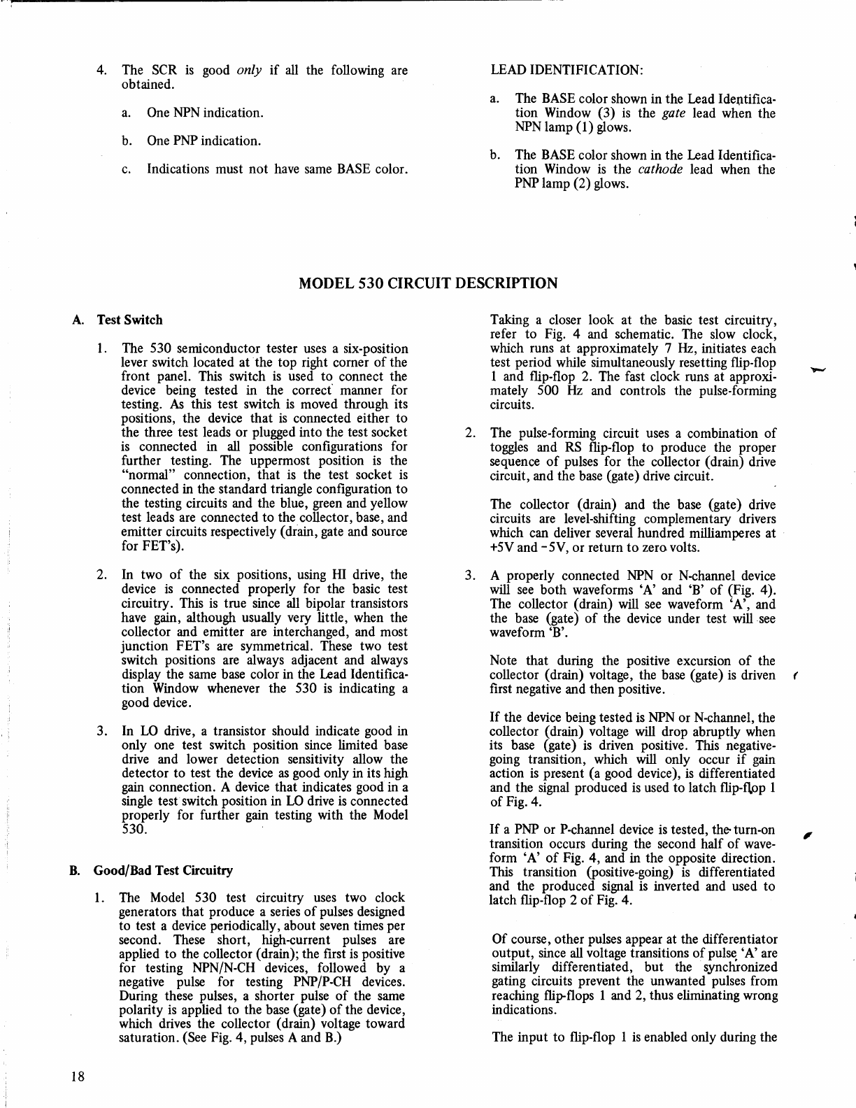
4. The SCR is good only if all the following are
obtained.
a. OneNPNindication.
b. One
PNP
indication.
c. Indicationsmust not havesameBASE color.
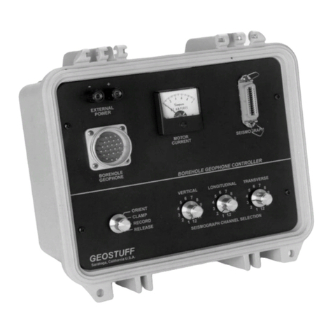
LEAD IDENTIFICATION:
a. The BASEcolor shown
in the I*ad ldeptifica-
tion Window (3) is the gate lead when the
NPNlamp(l) glows.
b. The BASEcolor shownin the kad ldentifica-
tion Window is the cathode lead when the
PNP
lamp(2) glows.
MODEL530CIRCUIT
DESCRIPTION
A. TestSwitch
The 530 semiconductortester usesa six-position
leverswitch locatedat the top right cornerof the
front panel. This switch is used to connect the
device being tested in the correct' manner for
testing. As this test switch is moved through its
positions, the devicethat is connected
either to
the three test leadsor plugged
into the testsocket
is connected in all possible configurations for
further testing. The uppermost position is the
"normal" connection, that is the test socket is
connected
in thestandardtriangle
configuration
to
the testingcircuits and the blue, green
and
yellow
testleadsareconnected
to thecollector,base,and
emitter circuits
respectively
(drain,gate
andsource
for FET's).
In two of the six positions,using HI drive, the
device is connected properly for the basic test
circuitry. This is true since all bipolar transistors
have gain, although usually very little, when the
collector and emitter are interchanged,
and most
junction FET's are symmetrical. Thesetwo test
switch positions are always adjacent and always
display the same
basecolor in the lBad Identifica-
tion Window whenever the 530 is indicating a
gooddevice.
In LO drive, a transistorshould indicategoodin
only one test switch position since limited base
drive and lower detection sensitivity allow the
detectorto test the device
as
good
only in its high
gainconnection.
A devicethat indicates
good
in a
singletestswitch position in LO driveis connected
properly for further gain testing with the Model
530.
B. Good/Bad TestCircuitry
l. The Model 530 test circuitry uses two clock
generators
that producea seriesof pulses
designed
to test a device
periodically,
aboutseven
times
per
second. These short, high-current pulses are
applied to the collector (drain); the first is positive
for testing NPN/N-CH devices, followed by a
negative pulse for testing PM/P-CH devices.
During thesepulses,
a shorter pulseof the same
polarity is appliedto thebase
(gate)
of thedevice,
which drivesthe collector (drain) voltagetoward
saturation.
(See
Fig.4, pulses
A andB.)
l8
Taking a closer look at the basictest circuitry,
refer to Fig. 4 and schematic.
The slow clock,
which runs at approximately 7 llz, initiates each
test period while simultaneouslyresettingflip-flop
I and flip-flop 2. The fast clock runs at approxi-
mately 500 Hz and controls the pulse-forming
circuits.
The pulse-formingcircuit usesa combination of
toggles and RS flip-flop to produce the proper
sequence
of pulsesfor the collector (drain) drive
circuit, andthe base
(gate)
drive
circuit.
The collector (drain) and the base (gate) drive
circuits arc level-shifting complementary drivers
which can deliver several
hundred milliamperesat
+5V and-5V, or returnto zerovolts.
A properly connected NPN or N-channel device
will see
both waveforms'A' and 'B' of (Fig. a).
The collector (drain) will seewaveform 'A', and
the base (gate) of the device under test will see
waveform'B'.
Note that during the positive excursion of the
collector (drain) voltage, the base
(gate) is driven
first negative
andthen positive.
If the device
beingtestedis NPNor N-channel,
the
collector (drain) voltage will drop abruptly when
its base (gate) is driven positive. This negative-
going transition, which will only occur if gain
action is present
(a good device),is differentiated
and the signalproduced is used
to latch flip-f[op 1
of Fig.4.
If a PNPor P-channel
deviceis tested,the turn-on
transition occurs during the secondhalf of wave-
form 'A' of Fig. 4, andin the opposite
direction.
This transition (positive-going) is differentiated
and the produced signalis inverted and usedto
latchflip-flop 2 of Fig.4.
Of course,
otherpulses
appearat the differentiator
output, since
all voltagetransitionsof pulsg'A' are
similarly differentiated, but the synchronized
gating circuits prevent the unwanted pulses
from
reachingflipflops I and2, thus eliminating wrong
indications.
The input to flip-flop I is enabledonly during the
l.
2.
3.
2.
3.


