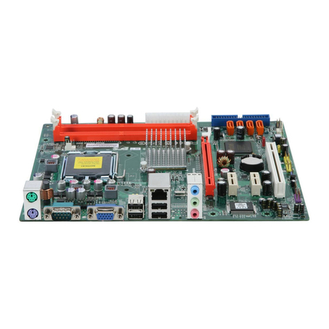
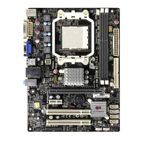
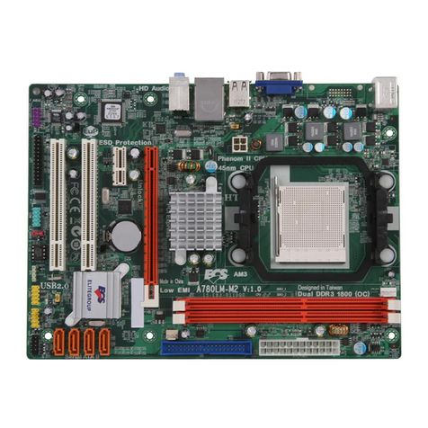
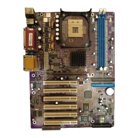
ECS NEATSX User manual

NEATsx


NEATSX
System Board
User's Manual

This User’s Guide and all accompanying software and documentation are copyrighted and all rights are
reserved. This product, including software and documentation, may not, in whole or in part, be copied, pho
tocopied, translated or reduced to any electronic or machine readable form without prior written consent
except for copies retained by the purchaser for backup purposes.
NO WARRANTY OR REPRESENTATION, EITHER EXPRESSED OR IMPLIED, IS MADE WITH RE
SPECT TO THIS DOCUMENTATION, ITS QUALITY, PERFORMANCE, MERCHANTABILITY, OR
FITNESS FOR A PARTICULAR PURPOSE. AS A RESULT, THE DOCUMENTATION IS LICENSED
“AS IS”, AND YOU,THE LICENSEE, ARE ASSUMING TOE ENTIRE RISK AS TO THEIR QUALITY
AND PERFORMANCE. TOE VENDOR RESERVES THE RIGHT TO REVISE THIS USER’S GUIDE
AND ANY ACCOMPANYING SOFTWARE AND DOCUMENTATION AND TO MAKE CHANGES
IN THE CONTENT WITHOUT OBLIGATION TO NOTIFY ANY PERSON OR ORGANIZATION OF
TOE REVISION OR CHANGE.
IN NO EVENT WILL TOE VENDOR BE LIABLE FOR DIRECT, INDIRECT, SPECIAL, INCIDENTAL,
OR CONSEQUENTIAL DAMAGES ARISING OUT OF TOE USE OR INABILITY TO USE THIS
PRODUCT OR DOCUMENTATION, EVEN IF ADVISED OF TOE POSSIBILITY OF SUCH DAM
AGES. IN PARTICULAR, TOE VENDOR SHALL NOT HAVE LIABILITY FOR ANY HARDWARE,
SOFTWARE, OR DATA STORED OR USED WITH THE PRODUCT, INCLUDING TOE COSTS OF
REPAIRING, REPLACING, OR RECOVERING SUCH HARDWARE, SOFTWARE, OR DATA.
Prepared by BSI Technical Documentation Services
Copyright 1989
All rights Reserved.
Manual Version 1.0
XT and AT are trademarks of International Business Machines Corporation

Contents
Introduction.......................................................................................1
Board Layout........................................................................3
Hardware...........................................................................................5
Specifications
.......................................................................
5
General......................................................................5
Memory Subsystem...................................................9
NEATsx ChipSet.......................................................18
ROM BIOS................................................................22
Peripheral Connections..............................................24
Setup.................................................................................... 27
Jumper Switches........................................................27
Before Installation Setup...........................................34
After Installation Setup.............................................36
Software........................................................................................... 41
Specifications.......................................................................41
AMI BIOS Setup Program........................................41
The NEATsx Disk.....................................................42
Setup....................................................................................45
AMI BIOS.................................................................45
Quiekset Setup Program............................................46
Installation & Operation..................................................................61
Care & Maintenance..........................................................................69
Installing Upgrades
..............................................................
.
............23

Checklist
Your NEATsx package should contain the following:
• The NEATsx mainboard
• One NEATsx floppy disk
• This manual
Im ortant!
If you do not intend to read this manual completely be certain
to at least review the Operation section. The NEATsx chip set
requires correct configuration information and if incorrectly setup
can disfunction. This section covers what to do in such an event. It
is also advisable to review the information on Software Setup.

Introduction
Introduction
The NEATsx system board is an cost effective compromise
between the power of a 32 bit internal architecture and the conven
ience of full compatibility with the IBM PC/AT and OS/2. The board
therefore allows the microprocessor to operate with all the advantages
of a ‘386 system, with multi tasking and multi user capabilities.
This manual has been designed to be useful for two purposes.
If your NEATsx is already set up in a functioning system you may
want to review the manual to familiarize yourself with the features of
the board and where things are. This will be helpful in the unlikely
event that you should ever have a problem with your NEATsx.
For those who want to alter the board’s configuration or up
grade it, the manual will serve as a guide to both procedure and speci
fications. While the necessary information is included in the manual,
we recommend that unless you feel confident of your ability to do the
work, it would be best to have your dealer or a local service shop do it
for you. If you decide to make alterations to the system yourself,
check to see that doing so will not violate your system warranty. If it
i loes you may want to have the work done by an authorized dealer.
1

Introduction
Board Layout
The diagrams on the next two pages shows the layout of the
NEATsx and the location of important components on the board.
NEATsx Board Layout Key
1: Keyboard Connector
2: J3: Battery connector
3: JP1: Video Mode selector
4: Power Su ly Connectors
5: JP2: Oscillator selector ( reset at factory)
6: JP4: On board/external Power Good signal selector
7:387SX Numeric Co rocessor socket
8: JP6: Memory bank number assignment selector
9 : Case connectors (Keylock, Turbo LED, Reset, S eaker, Turbo)
10: DIP memory banks; normally Banks 0/1
11: SIP memory banks; normally Banks 2/3
12: Ex ansion slots
13: J2: On board/external battery source selector
Note: Multi le elements are listed left to right. Also note
that all gra hics in this manual are oriented to this diagram
unless otherwise stated.
2

Introduction
Neat SX Board Layout

Introduction
Notes:

Hardware S ecifications
Hardware
S ecifications
The NEATsx is an 80386SX based mainboard that can run at
either 16 or 20 Mhz depending on the speed of installed memory
chips. It is a four layer board sized to fit in virtually any system unit
case from standard AT to tower cases. It can use any version of MS
DOS above version 3.0, in addition to the OS/2 and Xenix/Unix oper
ating systems. The NEATsx supports versions 3.2 and 4.0 of the Lo
tus Intel Microsoft (LIM) Expanded Memory Specification, more
commonly called EMS.
General S ecifications
Size
The NEATsx measures approximately 8.5 x 13 inches (22.5 x
33 cm) and has nine mounting holes placed so that the board can be
mounted in as wide a variety of cases as possible. The printed circuit
board is constructed with four layers to minimize radio frequency
interference.
5

Hardware S ecifications
80386SX CPU
The NEATsx uses an 80386sx microprocessor that operates
with 0.5 to 0.7 wait states at 16 Mhz with 100ns (100 nanosecond)
DRAMs and at 20 Mhz with 80ns DRAMs. The system can also be
software switched between low (8/10 Mhz) and high (16/20 Mhz)
speed modes. The operating speeds depend on the speed of DRAM in
stalled. By using the Quickset program provided on the NEATsx
floppy disk, you can select the desired microprocessor clock speed.
80387SX Math Co rocessor
The NEATsx has a socket for an 80387SX math coprocessor.
If an 80387SX chip is to be installed, make sure that it is clock speed
compatible with the NEATsx. The 80387SX 16 is required if the sys
tem is to operate at 16 Mhz.
Refer to the section on component installation for guidance re
garding the installation of the chip if you intend to do it yourself. Be
fore beginning a job, check whether or not doing the work yourself
will void your warranty.
6

Hardware S ecifications
The Ex ansion Bus
The NEATsx uses a modified eight slot AT expansion bus.
The bus is comprised of three 8 bit expansion slots and five 16 bit ex
pansion slots. These will accept all the common expansion cards that
conform to the standard slots. You should check to make sure that any
cards added are speed compatible with the NEATsx.
The slots each have two parallel rows of connecting pins.
When the connecting edge of an expansion card (the “golden fingers”)
is inserted between them, the slot pins grip the fingers and establish
the connection between the board and the card. It is important to keep
these connectors clean and dust free so that a proper connection can be
made. Look in the Care and Maintenance section for information relat
ing to this.
The Ex ansion Slots
8-bit XT Com atible
The three XT type eight bit expansion slots can be used for ex
pansion cards that do not require a sixteen bit data path. An example
of this type of card would be certain video display cards. These cards
are shorter than AT style cards; they have 62 pins divided into two
rows of 31 each.
7

Hardware S ecifications
16-bit Slots
The five sixteen bit expansion slots provide a wider data trans
mission pathway and will commonly be used by cards such as hard
disk controllers, network cards and many I/O expansion cards. The
slots are of two piece construction with one long section and one
short. The long sections are the same as the 8 bit slots. The additional
short sections have 36 pins divided into two rows of 18 each. These
two sections together make up a 16 bit data path. Cards that use these
slots must be plugged fully into both sections of the slot
8

Hardware S ecifications
Memory Subsystem
This section covers types of memory applicable to the
NEATsx and the structure of the memory subsystem.
The NEATsx can have up to eight megabytes of memory in
stalled on the mainboard. A number of different kinds of memory
chips or modules can be used. All of the memory on the mainboard
uses a 16 bit data path to connect to the microprocessor.
There are four memory banks on the NEATsx main board.
Two of these receive DIP DRAMs. The other two are for SIP memory
modules. Using jumper JP6 you can designate whether the SIP mod
ules or the DIP DRAMs should be banks zero and one. If you intend
to use DIP DRAMs, those sections of the memory subsystem must be
defined as banks zero and one. The other two SIP banks would then be
banks two and three. It’s not necessary, however, that these two SIP
banks be utilized. The point is that if you do use both DRAM chips
and SIP modules, it is the DRAM chips that must be designated as
banks zero and one.
If, however, only SIP modules will be used on the NEATsx
main board, then those must be defined as banks zero and one. Jumper
JP6 is for designating bank numbers. The physical banks obviously do
not change. The only change is in bank designations.
9

Hardware S ecifications
Ty es Of Memory
The NEATsx accepts two different DRAM sizes. The memory
subsystem accepts the following types of memory:
• 256 Kbit DIP DRAM. 512KB per bank. Configured as
two sets of two 44256 chips and one 41256 chip
See memory diagram for correct
placement
• 1 Mbit DIP DRAM. A full bank of eighteen 41000
chips totals 2 megabytes of memory.
• 256 Kbit SIP (Single In line Package) modules.
A full bank of two modules totals 512 kilobytes.
• 1 Mbit SIP modules. A full bank of two modules
totals 2 megabytes.
There are two forms of RAM noted above. The DIP DRAM
chips are single units that are installed individually. SIP modules are
mounted on a strip that plugs in as one unit. The two sections of each
SIP bank are physically in line, i.e., the two SIP modules for a bank
allign vertically. The side by side sections are of two different banks.
10

Hardware S ecifications
Notice that there are two sizes of RAM chips; 256 Kbit, and 1
Mbit. It is important to distinguish between bits and bytes here. The
bit measurement is for individual chips; the byte measurement is for
total memory size for a set of nine chips.
All the RAM chips function in sets of nine whether they are
installed individually or are part of a module. The individual chip
measurement, e.g., 256 Kbit, represents the total amount of memory in
one chip. Eight chips for memory plus one for parity checking make
up a set of nine.
A set of nine 256 Kbit chips or their equivalent will therefore
total 256 kilobytes of memory. The configuration of two 44256 chips
and one 41256 chip noted previously is equal to the configuration of
nine 256 Kbit chips. Both have a total memory of 256KB. One 44256
chip has the memory capacity of four 41256 chips. Nine 1 Mbit chips
will equal one megabyte of memory. Each DIP RAM bank on the
NEATsx has two sets of nine sockets. The figure on the next page
shows the socket configuration of the DIP RAM banks.
SIP modules come in two memory capacities: 256KB or 1MB
per module. One SIP module is equivalent to nine DRAM chips. Two
modules, therefore, are necessary for one memory bank.
11

Hardware S ecifications
■ 44256/41000
sockets
41000 sockets
41256/41000
sockets
NEATsx DIP RAM memory banks
12

Hardware S ecifications
Physical Organization
The NEATsx’s memory subsystem is divided into two parts
which are in turn have two sections. The sections are called banks.
There are four banks on the board, each with a capacity of two nine
chip sets. Two of the banks are for DIP DRAM chips, and two are for
SIP modules. The banks are numbered 0, 1,2, and 3, but their desig
nations depend on the setting of jumper JP6. The figures below show
the possible bank designations.
SIP RAM
banks
(the banks
run vertically)
Bank 3(1)
DIP RAM
banks
BankO
Bank 1
NEATsx memory bank organization
13

Hardware S ecifications
The NEATsx allows the installation of several types of RAM
in the same system. Six of the sockets for each DIP DRAM bank have
a dual design. The SIP banks are standard SIP sockets that will accept
modules with either 256 Kbit or 1 Mbit chips.
The result is a high degree of flexibility to install precisely the
amount and kind of memory desired. There are numerous possible
configurations. The table below lists the possible choices.
When installing or adding memory, the banks must be filled
beginning with bank zero, then bank one, and so on. Each bank can
contain only one kind of chip. Different types of chips can not be
mixed in the same bank except for the 44256/41256 configuration
mentioned earlier. A bank must be completely full to function.
Another nice feature of the NEATsx is that bank numbers can
be reassigned so that SIP modules can be used first. Normally the DIP
DRAM banks are assigned the zero and one positions. If you want to
use SIP modules exclusively, the bank numbering can be changed by
altering the setting of jumper JP6. The procedure to do this is ex
plained in the Hardware Setup section.
14
Table of contents
Other ECS Motherboard manuals
