ECS P4IBAD2 User manual

Preface
Copyright
This publication, including all photographs, illustrations and software, is protected un-
der international copyright laws, with all rights reserved. Neither this manual, nor any
of the material contained herein, may be reproduced without writtenconsent ofthe au-
thor.
Version 1.0
Disclaimer
The information in this document is subject to change without notice. The manufac-
turer makes no representations or warranties with respect to the contents hereof and
specifically disclaims any implied warranties of merchantability or fitness for any par-
ticular purpose. The manufacturer reserves the right to revise this publication and to
make changes from time to time in the content hereof without obligation of the manu-
facturer to notify any person of such revision or changes.
Trademark Recognition
Microsoft, MS-DOS and Windows are registered trademarks of Microsoft Corp.
MMX, Pentium, Pentium-II, Pentium-III, Celeron are registered trademarks of Intel
Corporation.
Other product names used in this manual are the properties of their respective owners
and are acknowledged.
Federal Communications Commission (FCC)
This equipment has been tested and found to comply with the limits for a Class B digi-
tal device, pursuant to Part 15 of the FCC Rules. These limitsare designed to provide
reasonable protection against harmful interference in a residential installation. This
equipment generates, uses, and can radiate radio frequency energy and, if not in-
stalled and used in accordance with the instructions, may cause harmful interference
to radio communications. However, there is no guarantee that interference will not oc-
cur in a particular installation. If this equipment does cause harmful interference to
radio or television reception, which can be determined by turning the equipment off
and on, the user is encouraged to try to correct the interference by one or more of the
following measures:
−Reorient or relocate the receiving antenna.
−Increase the separation between the equipment and the receiver.
−Connect the equipment onto an outlet on a circuit different from that to which
the receiver is connected.
−Consult the dealer or an experienced radio/TV technician for help.
Shielded interconnect cables and a shielded AC power cable must be employed with
this equipment to ensure compliance with the pertinent RF emission limits governing
this device. Changes or modifications not expressly approved by the system's manu-
facturer could void the user's authority to operate the equipment.

ii
Declaration of Conformity
This device complies with part 15 of the FCC rules. Operation is subject to the follow-
ing conditions:
−This device may not cause harmful interference, and
−This device must accept any interference received, including interference
that may cause undesired operation.
Canadian Department of Communications
This class B digital apparatus meets all requirements of the Canadian Interference-
causing Equipment Regulations.
Cet appareil numérique de la classe B respecte toutes les exigences du Réglement
sur le matériel brouilieur du Canada.
About the Manual
The manual consists of the following:
Chapter 1
Introducing the Mainboard Describes features of the mainboard,
and provides a shipping checklist.
Go to ⇒page 1
Chapter 2
Installing the Mainboard Describes installation of mainboard
components.
Go to ⇒page 7
Chapter 3
Using BIOS Provides information on using the BIOS
Setup Utility.
Go to ⇒page 25
Chapter 4
Using the Mainboard Software Describes the mainboard software.
Go to ⇒page 45

iii
T
TA
AB
BL
LE
E
O
OF
F
C
CO
ON
NT
TE
EN
NT
TS
S
Preface i
Features and Packing List Translations 錯誤! 尚未定義書籤。
CHAPTER 1 1
Introducing the Mainboard 1
Introduction............................................................................................................1
Checklist.................................................................................................................1
Standard Items...................................................................................................1
Features..................................................................................................................2
Choosing a Computer Case................................................................................4
Mainboard Components.......................................................................................5
CHAPTER 2 7
Installing the Mainboard 7
Safety Precautions................................................................................................7
Quick Guide...........................................................................................................7
Installing the Mainboard in a Case.....................................................................8
Checking Jumper Settings...................................................................................8
Setting Jumpers.................................................................................................8
Checking Jumper Settings .................................................................................9
Jumper Settings .................................................................................................9
Connecting Case Components.........................................................................10
Front Panel Connector.....................................................................................12
Installing Hardware.............................................................................................13
Installing the Processor ...................................................................................13
Installing MemoryModules............................................................................16
Installing a Hard Disk Drive/CD-ROM..........................................................17
Installing a Floppy Diskette Drive..................................................................18
InstallingAdd-on Cards...................................................................................19
Connecting Optional Devices..........................................................................21
ConnectingI/ODevices.....................................................................................23
External Connector Color Coding...................................................................24
CHAPTER 3 25
Using BIOS 25
About theSetup Utility........................................................................................25
The Standard Configuration............................................................................25
Entering the Setup Utility................................................................................26
Updating the BIOS..........................................................................................26
Using BIOS..........................................................................................................27
Standard CMOS Features................................................................................28
Advanced BIOS Features ................................................................................30

iv
Advanced Chipset Features.............................................................................32
Integrated Peripherals......................................................................................34
Power Management Setup...............................................................................37
PNP/PCI Configurations.................................................................................40
PC Health Status..............................................................................................41
Frequency/Voltage Control..............................................................................42
Load Fail-Safe Defaults Option......................................................................43
Load Optimized Defaults Option....................................................................43
Set Supervisor/User Password.........................................................................43
Save & Exit Setup Option...............................................................................44
Exit Without Saving........................................................................................44
CHAPTER 4 45
Using the Mainboard Software 45
About the Software CD-ROM............................................................................45
Auto-installing under Windows 98/ME/2000/XP............................................45
Running Setup.................................................................................................46
Manual Installation..............................................................................................48
Utility Software Reference.................................................................................48

C
Ch
ha
ap
pt
te
er
r
1
1
Introducing the Mainboard
I
In
nt
tr
ro
od
du
uc
ct
ti
io
on
n
Congratulations on purchasing the P4IBAD2 mainboard. The P4IBAD2 main-
board is an ATX mainboard that uses a 4-layer printed circuit board and
measures 304.8 mm x 220 mm. The mainboard features a mPGA478 Socket
that accommodates Intel Pentium 4 Willamette/ Northwood processors sup-
porting system speeds up to 400/533 MHz and data bus bandwidths up to 3.2
GB/s.
The mainboard comes with a full set of I/O features conveniently integrated on
the rear I/O panel, includingsupport for PS/2 keyboard and mouse connectors,
two USB ports, a LAN connector, two high-speed serial port, an EPP/ECP
parallel port, audio jacks for microphone, line-in, line-out and CD-in and a
game port, as well as supporting Plug and Play.
The P4IBAD2 incorporates the Intel i82845 (MCH) and the Intel 82801BA
(ICH2) chipsets, which supports 2.5V DDR DRAM, 2X/4X AGP (1.5V only),
andtheAC’97 codec.
C
Ch
he
ec
ck
kl
li
is
st
t
Compare the mainboard’s package contents with the following checklist:
Standard Items
•One mainboard
•One diskette drive ribbon cable
•One IDE drive ribbon cable
•Software support CD
•Retention Module
•This user’s manual
2
F
Fe
ea
at
tu
ur
re
es
s
ProcessorThe P4IBAD2 mainboard uses a mPGA478 Socket that has
the following features:
•Accommodates Intel Pentium 4 478-pins CPU
•Supports a system bus (FSB) of 400/533 (enhanced)
MHz
•Supports 3.2 GB/s data bus bandwidth
Chipset Intel’s innovative i82845 (MCH) and 82801BA (ICH2) chipsets
are based on an innovative and scalable architecture with
proven reliability and performance. A few of the advanced
features of the chipsets are:
•Host interface controller supports 400 MHz frontside (sys-
tem) bus frequency
•Supports 266 MHz DDR SDRAM devices
•Supports a max of 2 Double-Sided DIMMs (4 rows popu-
lated) with unbuffered DDR266 (w/ or w/out ECC).
•Supports a maximum memory bandwidth of 2.1 GB/s with
DDR266
•AGP controller is AGP 2.0 compliant and supports 2x/4x
Fast Write Protocol (1.5V only)
•PCI IDE controller supports PCI bus mastering, PIO
modes 0~4, and UDMA 33/66/100
•Two USB controllers double the bandwidth to 24 Mbps
across four ports
•Integrated AC’ 97 audio that supports full surround sound
with up to six channels
Additional key features include support for an AC 97 link for audio
and modem, hardware monitoring, and ACPI/OnNow power man-
agement.
Memory •Supports DDR up to 200/266/333 (enhanced) MHz DDR
SDRAM memory module
•Accommodates two unbuffered 2.5V 184-pin slots
•Each slot supports up to 1 GB with a total maximum
capacity of 2 GB
AGP The P4IBAD2 includes a 4xAGP slot that provides four times the
bandwidth of the original AGP specification. AGP technology pro-
vides a direct connection between the graphics sub-systemand
the processor so that the graphics do not have to compete for
processor time with other devices on the PCI bus.
Audio •Compliant with AC’97 codec
•Supports 4.1/5.1 speakers, C3DX positional audio in 4/6
channel speaker mode
•6 channel DAC for AC3® 5.1channel purpose
•Professional digital audio interface supporting 24-bit
SPDIF IN and OUT (44.1K and 48K format)
•Compatible with legacy audio SBPRO™
USB 2.0
(optional) The built-in VIA VT6202 PCI USB 2.0 Controller is compliant
with Universal Serial Bus Specification Revision 2.0.
The USB 1.1 connectors and other full speed cables can sup-
port the higher speed of USB 2.0 without any changes.
The chipset has the following advanced USB features:
3
•Integrated multi-PCI function in a single chip including two
UHCI host Controllers for low/full speed data transactions
and one EHCI host controller for high-speed data transac-
tions
•Four downstream ports, each port providing full support
for low/full/high speed data rates
•YSB device wake-up function support
•Legacy function support
•PCI Specification Revision 2.2 compliant
•PCI Bus Power Management Interface Revision 1.1 com-
pliant
•3.3V/2.5V multi-power supply and 3.3V suspend power
for wake-up function
Expansion
Options The mainboard comes with the following expansion options:
•Six 32-bit PCI slots
•One 4xAGP slot (support 1.5V only)
•One Communications Network Riser (CNR) slot
•Two IDE connectors which support four IDE channels and
a floppy disk drive interface
The P4IBAD2 supports Ultra DMA bus mastering with transfer
rates of 33/66/100 MB/sec.
Integrated I/O The mainboard has a full set of I/O ports and connectors:
•Two PS/2 ports for mouse and keyboard
•Two serial ports
•One parallel port
•One MIDI/game port
•Two USB ports
•Audio jacks for microphone, line-in and line-out
BIOS
Firmware This mainboard uses Award BIOS that enables users to con-
figure many system features including the following:
•Power management
•Wake-up alarms
•CPU parameters and memory timing
•CPU and memory timing
The firmware can also be used to set parameters for different
processor clock speeds.

4
C
Ch
ho
oo
os
si
in
ng
g
a
a
C
Co
om
mp
pu
ut
te
er
r
C
Ca
as
se
e
There are many types of computer cases on the market. The mainboard com-
plies with the specifications for the ATX system case. Some features on the
mainboard are implemented by cabling connectors on the mainboard to indi-
cators and switches on the system case. Ensure that your case supports all
the features required. The mainboard can support one or two floppy diskette
drives and four enhanced IDE drives. Ensure that your case has sufficient
power and space for all the drives that you intend to install.
Most cases have a choice of I/O templates in the rear panel. Make sure that
the I/O template in the case matches the I/O ports installed on the rear edge
of the mainboard.
This mainboard has an ATX form factor of 304.8 mm x 220 mm. Choose a
case that accommodates this form factor.

5
M
Ma
ai
in
nb
bo
oa
ar
rd
d
C
Co
om
mp
po
on
ne
en
nt
ts
s

6
Table of Mainboard Components
Label Component
AGP1 Accelerated Graphics Port (supports 1.5V 4x AGP card only)
ATX1 Standard 20-pin ATX power connector
AUDIO1 Mic/SpeakerOut header
BAT1 Three volt realtime clock battery
CASFAN1 Case fan connector
CDIN1 CD-in connector (Panasonic)
CDIN2 CD-in connector (Sony)
CHS1 Chassis Detect Intrusion
CPUFAN1 Cooling fan for CPU
CNR1 Communications Networking Riser slot
CPU Socket CPU socket (mPGA478)
DIMM1 ~ DIMM2 Two 184-pin DDR sockets
FDD1 Floppy disk drive connector
IDE 1 Primary IDE channel
IDE 2 Secondary IDE channel
JP1 Clear CMOS jumper
JP2 BIOS protect jumper
JP4 Onboard USB jumper
LSJ1 Single color LED header (comply with OEM specs. only)
PANEL1 Front panel connectors for case switches and LEDs
PCI1 ~ PCI6 Six 32-bit add-on card slots
PWRFAN1 Power fan connector
SIR1 Serial IR port
SPEAKER1 Speaker connector
SJ1 Single color LED header
USB1 Front panel USB headers
This concludes Chapter 1. The next chapter explains how to install the main-
board.

7
C
Ch
ha
ap
pt
te
er
r
2
2
Installing the Mainboard
S
Sa
af
fe
et
ty
y
P
Pr
re
ec
ca
au
ut
ti
io
on
ns
s
Follow these safety precautions when installing the mainboard:
•Wear a grounding strap attached to a grounded device to avoid
damage from static electricity.
•Discharge static electricity by touching the metal case of a safely
grounded object before working on the mainboard.
•Leave components in the static-proof bags they came in.
•Hold all circuit boards by the edges. Do not bend circuit boards.
Q
Qu
ui
ic
ck
k
G
Gu
ui
id
de
e
This Quick Guide suggests the steps you can take to assemble your system
with the mainboards.
The following table provides a reference for installing specific components:
Locating Mainboard Components Go to page 5
Installing the Mainboard in a Case Go to page 8
Setting Jumpers Go to page 8
Installing Case Components Go to page 10
Installing the CPU Go to page 13
Installing Memory Go to page 16
Installing a HDD and CD-ROM Drive Go to page 17
Installing a FDD Go to page 18
Installing Add-on Cards Go to page 19
Connecting Options Go to page 21
Connecting Peripheral (I/O) Devices Go to page 23
8
I
In
ns
st
ta
al
ll
li
in
ng
g
t
th
he
e
M
Ma
ai
in
nb
bo
oa
ar
rd
d
i
in
n
a
a
C
Ca
as
se
e
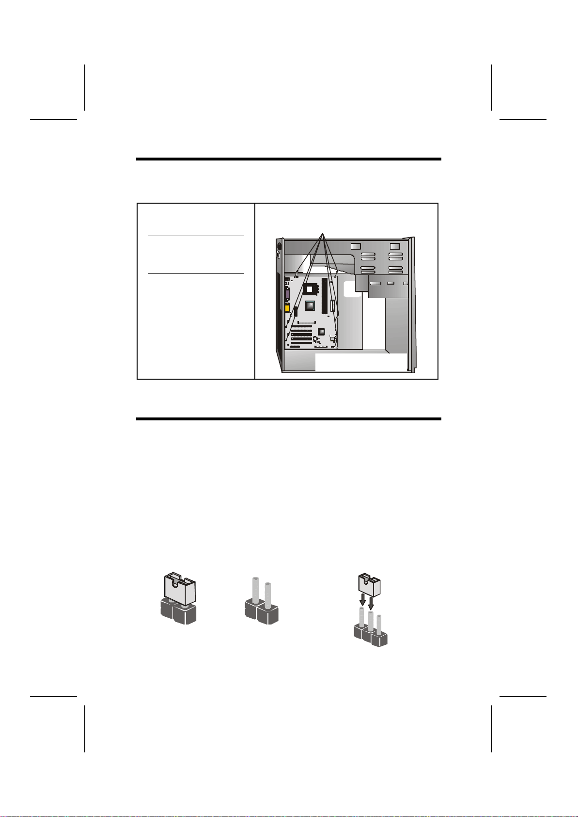
Refer to the following illustration and instructions for installing the mainboard
in a case:
This illustration shows an ex-
ample of a mainboard being
installed in a tower-type case:
Note: Do not overtighten
the screws as this
can stress the main-
board.
Most system cases have
mounting brackets installed in
the case, which correspond to
the holes in the mainboard.
Place the mainboard over the
mounting brackets and secure
the mainboard onto the mount-
ing brackets with screws.
2. Secure the mainboard with
screwswhereappropriate.
1. Place the mainboard
over the mounting brackets.
Ensure that your case has an I/O template that supports the I/O ports and
expansion slots on your mainboard.
C
Ch
he
ec
ck
ki
in
ng
g
J
Ju
um
mp
pe
er
r
S
Se
et
tt
ti
in
ng
gs
s
This section explains how to set jumpers for correct configuration of the main-
board.
Setting Jumpers
Use the mainboard jumpers to set system configuration options. Jumpers with
more than one pin are numbered. When setting the jumpers, ensure that the
jumper caps are placed on the correct pins.
The illustrations below show a 2-pin jumper.
When the jumper cap is placed on both pins,
the jumper is SHORT. If you remove the
jumper cap, or place the jumper cap on just
one pin, the jumper is OPEN.
This illustration shows a 3-pin
jumper. Pins 1 and 2 are SHORT.
Short Open
12
3
9
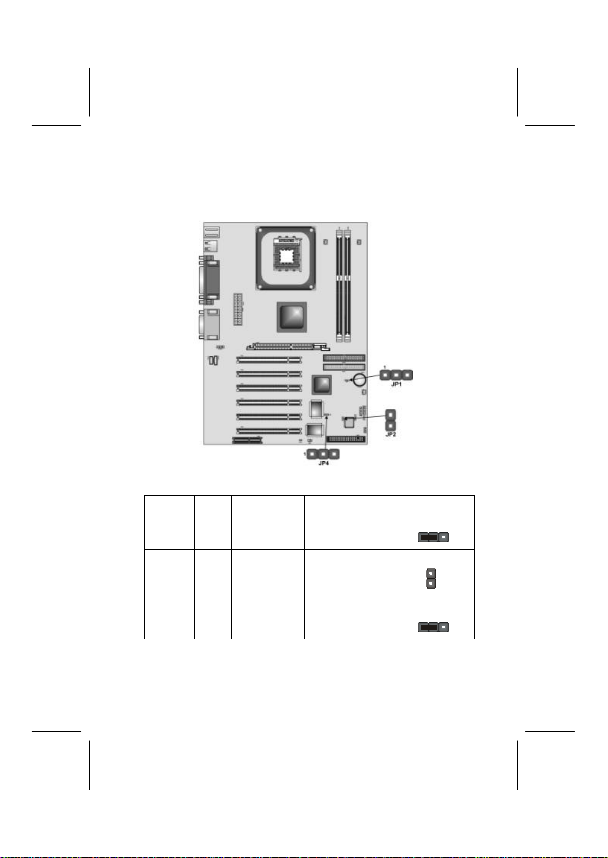
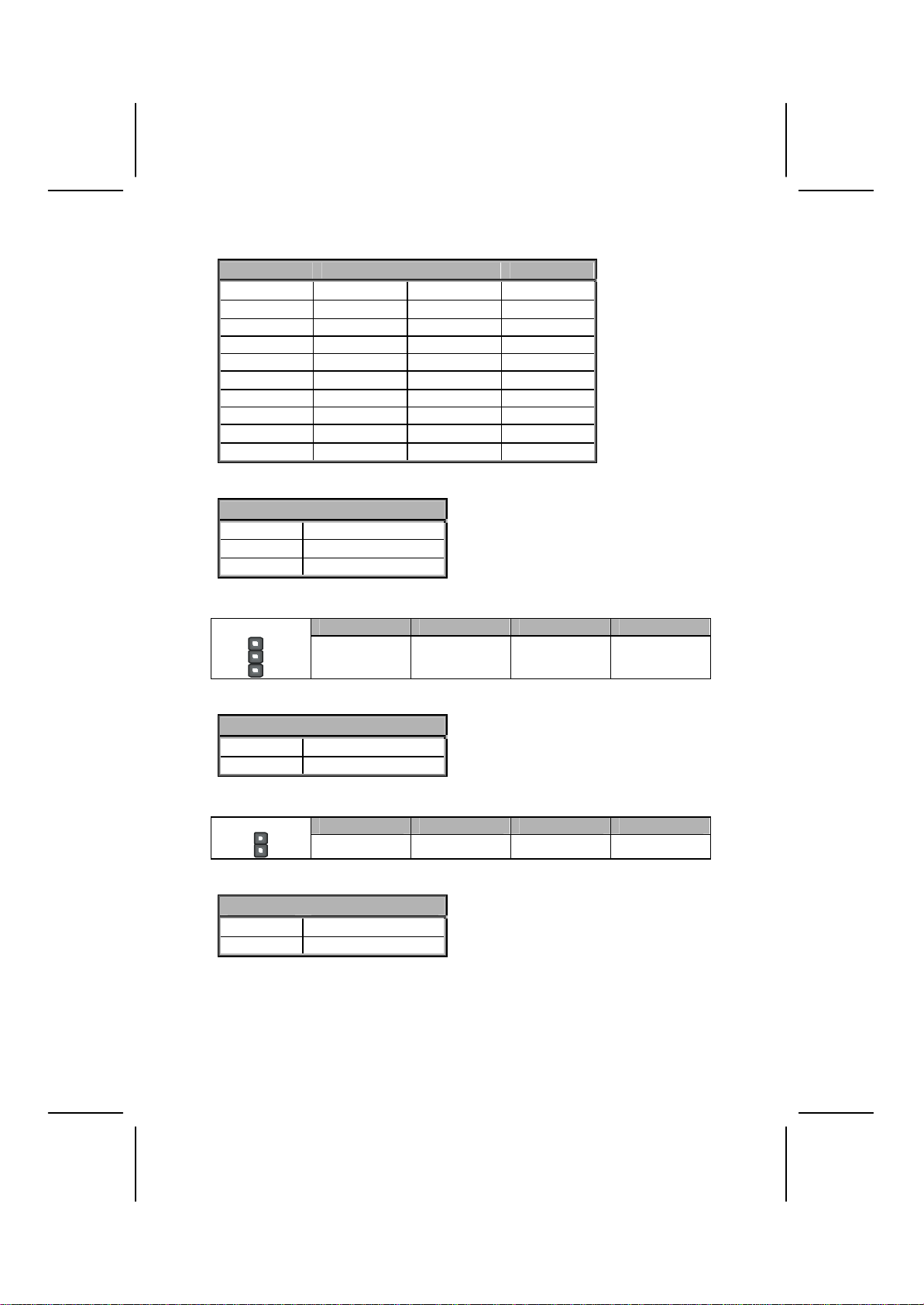
Checking Jumper Settings
The following illustration shows the location of the mainboard jumpers. Pin 1 is
labeled.
Jumper Settings
Jumper
Type Description Setting (default)
JP1 3-pin Clear CMOS 1-2: Normal
2-3: Clear
JP
1
1
JP2 2-pin BIOS flash
protection Short: Flash protect
Open: Flash JP2
JP4 3-pin Disable USB
function 1-2: Enabled
2-3: Disabled
JP
4
1
JP1 –Use this jumper to clear the contentsof the CMOS memory. You may
need to clear the CMOS memory if the settings in the Setup Utility
are incorrect and prevent your mainboard from operating. To clear
the CMOS memory, disconnect all the power cables from the main-
board and then move the jumper cap into the CLEAR setting for a

10
few seconds.
JP2 –Enables you to prevent the BIOS from being updated (flashed). Open
the jumper if you are going to update your BIOS. After updating the
BIOS, short the jumper to protect the BIOS from being flashed. For
instructions on updating the BIOS refer to Chapter 3.
JP4 –Use this jumper to enable or disable the onboard USB function.
C
Co
on
nn
ne
ec
ct
ti
in
ng
g
C
Ca
as
se
e
C
Co
om
mp
po
on
ne
en
nt
ts
s
After you have installed the mainboard into a case, you can begin connecting
the mainboard components. Refer to the following:
1. Connect the case power
supply connector to ATX1.
2. Connect the CPU cooling
fan cable to CPUFAN1.
3. Connect the case cooling
fan connector to
CASFAN1.
4. Connect the auxiliary
power supply cooling fan
connector to PWRFAN1.
5. Connect the case speaker
cable to SPEAKER1.
6. If your case has a case
open alarm cable, connect
it to CHS1.
7. Connect the case LED cable to SJ1/LSJ1.
8. Connect the case switches and indicator to PANEL1.
CPUFAN1/PWRFAN1/CASFAN1: FAN Power Connectors
Pin Signal Name Function
1GND System Ground
2+12V Power +12V
3Sense Sensor
11
ATX1: ATX 20-pin Power Connector
Pin Signal Name
Pin Signal Name
1+3.3V 11 +3.3V
2+3.3V 12 -12V
3Ground 13 Ground
4+5V 14 PS ON#
5Ground 15 Ground
6+5V 16 Ground
7Ground 17 Ground
8PWRGD18 +5V
9+5VSB 19 +5V
10 +12V 20 +5V
SJI: Single-color LED header
Pin Signal Name
1ACPI LED
2ACPI LED
35VSB
ACPI LED function:
S0 S1 S3 S4/S5
SJ11
Light Blinking Blinking Dark
LSJI: Single color LED header(for OEM customers only)
Pin Signal Name
15VSB
2SUSLED-Y
ACPI LED function:
S0 S1 S3 S4/S5
LSJ1
Dark Dark Light Dark
CHS1: Chassis Intrusion Detect
Pin 1-2Function
Short Case Open
Open Case Close
12
Front Panel Connector
The front panel connector (PANEL1) provides a standard set of switch and
LED connectors commonly found on ATX or micro-ATX cases. Refer to the
table below for information:
PANEL1
Pin
Signal Name
Function
1HD_LED_P Hard disk LED pull up (330 ohm) to +5V
2FP PWR/SLP MSG LED pull up (330 ohm) to +5V
3HD_LED_N Hard disk active LED
4GND Ground
5RST_SW_N Reset Switch low reference pull down
(100 ohm) to GND
6PWR_SW_P Power Switch high reference pull up
(10000 ohm) to +5V
7RST_SW_P Reset Switch high reference pull up
(1000 ohm) to +5V
8PWR_SW_N Power Switch high reference pull down
(100 ohm) to GND
9RSVD Reserved (do not use)
10
NC No pin
Hard Drive Activity LED
Connecting pins 1 and 3 to a front panel mounted LED provides visual indica-
tion that data is being read from or written to the hard drive. For the LED to
function properly, an IDE drive should be connected to the onboard IDE inter-
face. The LED will also show activity for devices connected to the SCSI (hard
drive activity LED) connector.
Power / Sleep / Message Waiting LED
Connecting pins 2 and 4 to a single-or dual-color, front panel mounted LED
provides power on/off, sleep, and message waiting indication.
Reset Switch
Supporting the reset function requires connecting pins 5 and 7 to a momen-
tary-contact switch that is normally open. When the switch is closed, the board
resets and runs POST.
Power Switch
Supporting the power on/off function requires connecting pins 6 and 8 to a
momentary-contact switch that is normally open. The switch should maintain
contact for at least 50 ms to signal the power supply to switch on or off. The
time requirement is due to internal debounce circuitry. After receiving a power
on/off signal, at least two seconds elapses before the power supply recog-
nizes another on/off signal.

13
I
In
ns
st
ta
al
ll
li
in
ng
g
H
Ha
ar
rd
dw
wa
ar
re
e
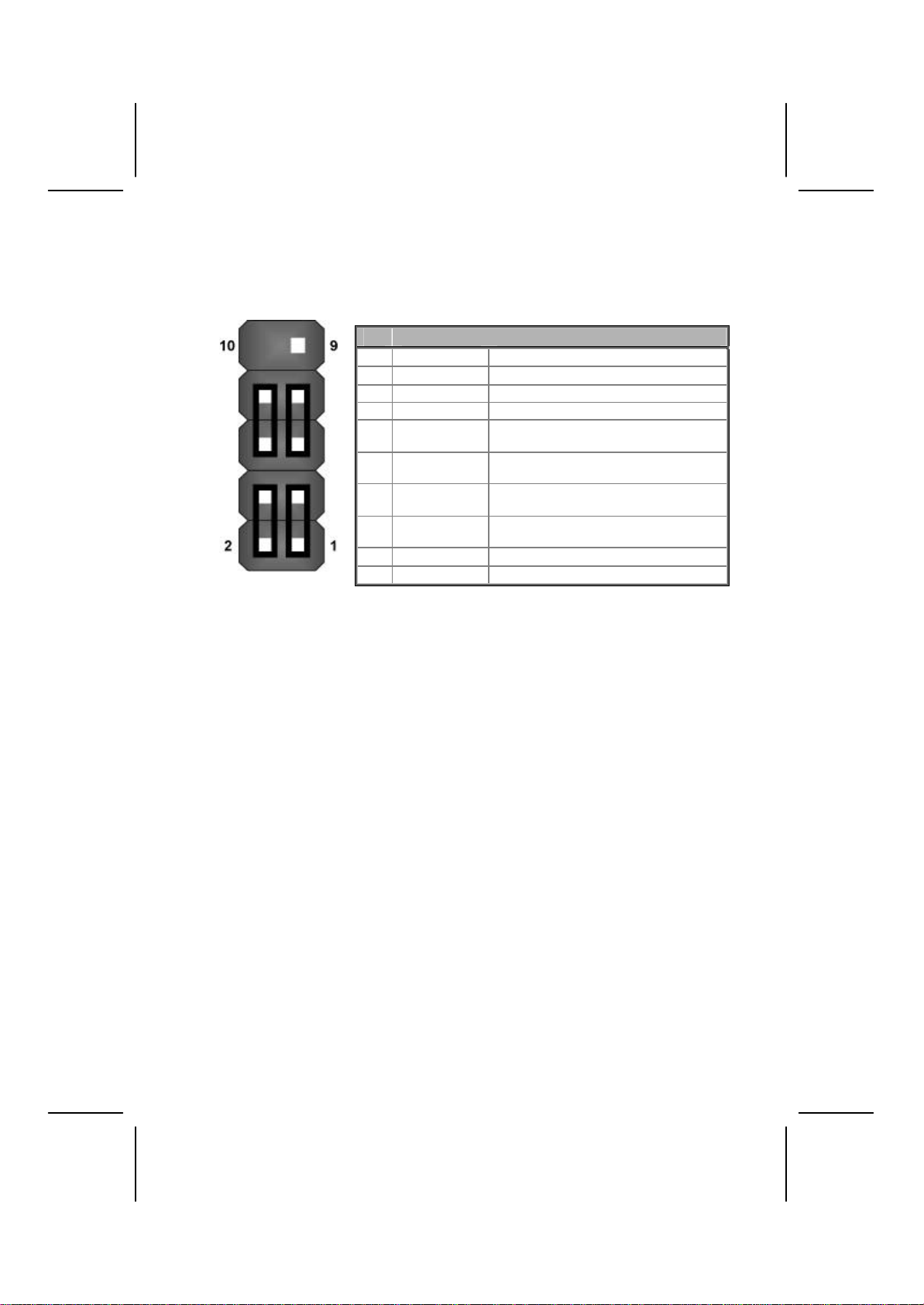
Installing the Processor
Caution: When installing a CPU heatsink and cooling fan make sure that
you DO NOT scratch the mainboard or any of the surface-mount resistors
with the clip of the cooling fan. If the clip of the cooling fan scrapes
across the mainboard, you may cause serious damage to the mainboard
or its components.
On most mainboards, there are small surface-mount resistors near the
processor socket, which may be damaged if the cooling fan is carelessly
installed.
Avoid using cooling fans with sharp edges on the fan casing and the
clips. Also, install the cooling fan in a well-lit work area so that you can
clearly see the mainboard and processor socket.
Before installing the Processor
This mainboard automatically determines the CPU clock frequency and sys-
tem bus frequency for the processor. You may be able to change these
settings by making changes to jumpers on the mainboard, or changing the
settings in the system Setup Utility. We strongly recommend that you do not
overclock processors or other components to run faster than their rated speed.
Warning: Overclocking components can adversely affect the reliability of
the system and introduce errors into your system. Overclocking can per-
manently damage the mainboard by generating excess heat in
components that are run beyond the rated limits.
This mainboard has an mPGA478 socket. When choosing a processor, con-
sider the performance requirements of the system. Performance is based on
the processor design, the clock speed and system bus frequency of the proc-
essor, and the quantity of internal cache memory and external cache memory.
14
CPU Installation Procedure
The following illustration shows CPU installation components:
Note: The pin-1 corner is marked with an arrow
Follow these instructions to install the Retention Module and CPU:
1. Remove the existing retention module (if applicable).
2. Position the backplate
against the underside of
the mainboard, secure
the 4 screws firmly on
the retention module.
Note: Do not over tighten
the screws.
3. Install your CPU. Pull up
the lever away from the
socket and lift up to 90-
degree angle.
15
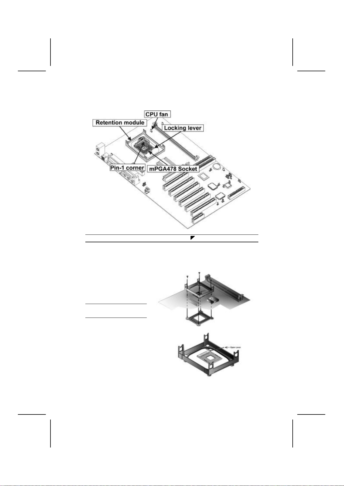
4. Locate the CPU cut
edge (the corner with the
pinhole noticeably miss-
ing). Align and insert the
CPU correctly.
5. Press the lever down.
6. Apply thermal grease on top of the CPU.
7. Put the CPU Fan down
on the retention module
and snap the four reten-
tion legs of the cooling
fan into place.
8. Flip the levers over to lock the heat sink in place.
9. Connect the CPU Cool-
ing Fan power cable to
the CPUFAN1 connec-
tor. This completes the
installation.
Note:CPU fan and heatsink installation procedures may vary with the type of
CPU fan/heatsink supplied. The form and size of fan/heatsink may also
vary.
16
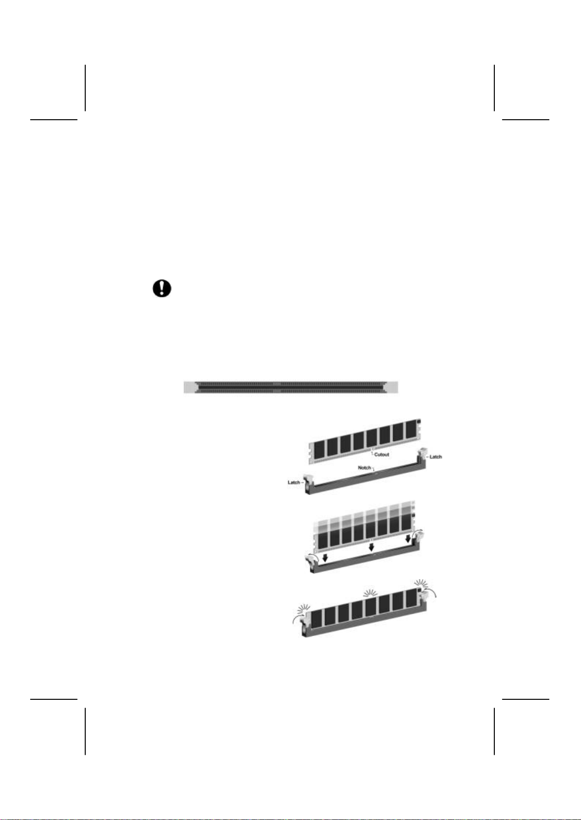
Installing Memory Modules
This mainboard accommodates 184-pin 2.5V unbuffered Double Data Rate
(DDR) SDRAM memory modules. The memory chips must be standard or
registered SDRAM (Synchronous Dynamic Random Access Memory).
The mainboard can accommodate two memory modules. You must install at
least one module in any of the two slots. Each module can be installed with 64
MB to 512 MB of memory with a total capacity of 2GB. It also offers enhanced
support for DDR333 memory modules. You can install DDR333 memory mod-
ule that can run up at 166 MHz memory bus. But there is no guarantee that
this will work properly with the mainboard.
Do not remove any memory module from its antistatic packaging until
you are ready to install it on the mainboard. Handle the modules only by
their edges.Do not touch the components or metal parts. Always wear
a grounding strap when you handle the modules.
Installation Procedure
Refer to the following to install the memory modules.
1. This mainboard supports unbuffered DDR SDRAM only. Do not attempt to
insert any other type of DDR SDRAM into the slots.
2. Push the latches on each side of the DIMM slot down.
3. Align the memory module with
the slot. The DIMM slots are
keyed with notches and the
DIMMs are keyed with cutouts
so that they can only be in-
stalled correctly.
4. Check that the cutouts on the
DIMM module edge connector
match the notches in the
DIMM slot.
5. Install the DIMM module into
the slot and press it firmly
down until it seats correctly.
The slot latches are levered
upwards and latch on to the
edges of the DIMM.
6. Install any remaining DIMM modules.
Table of contents
Other ECS Motherboard manuals


