ECS P4VXASD User manual

Preface
Copyright
This publication, including all photographs, illustrations and software,
is protected under international copyright laws, with all rights re-
served. Neither this manual, nor any of the material contained herein,
may be reproduced without written consent of the author.
Version 1.0b
Disclaimer
The information in this document is subject to change without notice.
The manufacturer makes no representations or warranties with re-
spect to the contents hereof and specifically disclaims any implied
warranties of merchantability or fitness for any particular purpose.
The manufacturer reserves the right to revise this publication and to
make changes from time to time in the content hereof without obliga-
tion of the manufacturer to notify any person of such revision or
changes.
Trademark Recognition
Microsoft, MS-DOS and Windows are registered trademarks of Mi-
crosoft Corp.
MMX, Pentium, Pentium-II, Pentium-III, Pentium 4, Celeron are reg-
istered trademarks of Intel Corporation.
Other product names used in this manual are the properties of their
respective owners and are acknowledged.
Copyright © 2001
All Rights Reserved
P4VXASD, V1.0b

ii
Federal Communications Commission (FCC)
This equipment has been tested and found to comply with the limits
for a Class B digital device, pursuant to Part 15 of the FCC Rules.
These limits are designed to provide reasonable protection against
harmful interference in a residential installation. This equipment gen-
erates, uses, and can radiate radio frequency energy and, if not
installed and used in accordance with the instructions, may cause
harmful interference to radio communications. However, there is no
guarantee that interference will not occur in a particular installation. If
this equipment does cause harmful interference to radio or television
reception, which can be determined by turning the equipment off
and on, the user is encouraged to try to correct the interference by
one or more of the following measures:
−Reorient or relocate the receiving antenna.
−Increase the separation between the equipment and the
receiver.
−Connect the equipment onto an outlet on a circuit different
from that to which the receiver is connected.
−Consult the dealer or an experienced radio/TV technician
for help.
Shielded interconnect cables and a shielded AC power cable must
be employed with this equipment to ensure compliance with the per-
tinent RF emission limits governing this device. Changes or
modifications not expressly approved by the system's manufacturer
could void the user's authority to operate the equipment.

iii
Declaration of Conformity
This device complies with part 15 of the FCC rules. Operation is sub-
ject to the following conditions:
−This device may not cause harmful interference, and
−This device must accept any interference received, includ-
ing interference that may cause undesired operation.
Canadian Department of Communications
This class B digital apparatus meets all requirements of the Cana-
dian Interference-causing Equipment Regulations.
Cet appareil numérique de la classe B respecte toutes les exigences
du Réglement sur le matériel brouilieur du Canada.

iv
About the Manual
The manual consists of the following:
Chapter 1
Introducing the Mainboard
Describes features of the main-
board, and provides a shipping
checklist.
Go to ⇒page 1
Chapter 2
Installing the Mainboard
Describes installation of main-
board components.
Go to ⇒page 7
Chapter 3
Using BIOS
Provides information on using
the BIOS Setup Utility.
Go to ⇒page 34
Chapter 4
Using the Mainboard Software
Describes the mainboard soft-
ware.
Go to ⇒page 50
Appendix A
Setting Jumpers
Provides a reference to the
jumpers on the mainboard.
Go to ⇒page 57

v
T
TA
AB
BL
LE
E
O
OF
F
C
CO
ON
NT
TE
EN
NT
TS
S
Preface i
CHAPTER 1 1
Introducing the Mainboard 1
Introduction ......................................................................................1
Checklist ..........................................................................................2
Standard Items ..................................................................................... 2
Optional Accessories ........................................................................... 2
Features...........................................................................................3
Mainboard Components ..................................................................5
Choosing a Computer Case ............................................................6
CHAPTER 2 7
Installing the Mainboard 7
Safety Precautions...........................................................................7
Quick Guide .....................................................................................8
Checking Jumper Settings...............................................................9
Setting Jumpers ................................................................................... 9
Checking Jumper Settings ................................................................. 10
Jumper Settings ..................................................................................11
Installing the Mainboard in a Case ................................................14
Connecting Case Components......................................................15
The Panel1 and Panel2 Connectors ................................................... 16
Installing Hardware........................................................................17
Installing the Processor...................................................................... 17
Installing Memory Modules .............................................................. 21
Installing a Hard Disk Drive/CD-ROM............................................. 23
Installing a Floppy Diskette Drive..................................................... 26
Installing Add-on Cards..................................................................... 27
Connecting Optional Devices............................................................ 29
Connecting I/O Devices.................................................................32
External Connector Color Coding ..................................................... 33
CHAPTER 3 34
Using BIOS 34
About the Setup Utility ...................................................................34
The Standard Configuration .............................................................. 35
Entering the Setup Utility.................................................................. 36
Using BIOS ....................................................................................37

vi
Standard CMOS Setup Page.............................................................. 37
Advanced Setup Page........................................................................ 39
Power Management Setup Page ........................................................ 42
PCI / Plug and Play Setup Page......................................................... 44
Load Optimal Settings....................................................................... 45
Load Best Performance Settings........................................................ 45
Features Setup Page........................................................................... 45
CPU PnP Setup Page ......................................................................... 47
Hardware Monitor Page .................................................................... 48
Change Password............................................................................... 49
Exit .................................................................................................... 49
CHAPTER 4 50
Using the Mainboard Software 50
About the Software CD-ROM ........................................................50
Auto-installing under Windows 98 .................................................51
Manual Installation.........................................................................54
Utility Software Reference .............................................................54
APPENDIX A 57
Setting Jumpers 57
Jumper Settings ................................................................................. 57
The Panel1 and Panel2 Connectors ................................................... 60

C
Ch
ha
ap
pt
te
er
r
1
1
Introducing the Mainboard
I
In
nt
tr
ro
od
du
uc
ct
ti
io
on
n
This mainboard has a Socket 423 for the Intel Pentium 4
type processors supporting front side bus (FSB) speeds up to
400 MHz.
This mainboard has the VIA VT8753 (P4X266) Northbridge
and VT8233 Southbridge chipsets that support AC’97 audio
codec, and provide Ultra DMA 33/66/100 function. This
mainboard has four 32-bit PCI slots, one 4xAGP slot, one
CNR (Communications and Networking Riser) slot, and an
onboard 10BaseT/100BaseTX Network interface (optional).
In addition, this mainboard has a full set of I/O ports including
two PS/2 ports for mouse and keyboard, two serial ports, one
parallel port, one MIDI/game port and six USB ports (two
backpanel ports, onboard USB headers providing four extra
ports).
By means of the Extended USB Module connected to the
mainboard, you can make four extra USB ports.
This mainboard is an ATX mainboard that uses a 4-layer
printed circuit board and measures 305 x 244 mm.

2
C
Ch
he
ec
ck
kl
li
is
st
t
Compare the mainboard’s package contents with the following
checklist:
Standard Items
•One mainboard
•The User’s Manual
•One diskette drive ribbon cable
•One IDE drive ribbon cable
•Software support CD
•One Retention Module
Optional Accessories
You can purchase the following optional accessories for this
mainboard.
•Extended USB module
•CNR v.90 56K Fax/Modem card
3
F
Fe
ea
at
tu
ur
re
es
s
Processor •The PGA Socket 423
•Accommodates Intel Pentium 4 CPUs
•Supports a front-side bus (FSB) of 400 MHz
Chipset There are VT8753 Northbridge and VT8233
Southbridge in this chipset in accordance with an
innovative and scalable architecture with proven
reliability and performance. A few of the chipset’s
advanced features are:
•An advanced V-Link memory controller archi-
tecture that provides the bandwidth up to 266
MB/s and performance necessary for even
the most demanding Internet and 3D graph-
ics
•Support for an 4xAGP interface providing
vivid 3D graphics and video performance
•An ATA 100 interface on the chipset, which
helps boost system performance by providing
a high-speed connection to ATA 100 Hard
Disk Drives, delivering maximum sustained
data transfer rates of 100 MB/sec
Additional key features include support for six
USB ports, an AC 97 link for audio and modem,
hardware monitoring, and ACPI/OnNow power
management.
Memory The mainboard accommodates 2 DDR + 2 SDR
168 pin, 3.3V DIMM sockets with a total capacity
of 2 GB system memory.
VGA This mainboard includes a 4xAGP slot that pro-
vides eight times the bandwidth of the original
AGP specification. AGP technology provides a
direct connection between the graphics sub-
system and memory so that the graphics do not
have to compete for processor time with other
devices on the PCI bus.

4
AC 97 Audio
Codec
The AC’97 Audio codec is compliant with the AC’
97 2.1 specification, and supports 18-bit ADC
(Analog Digital Converter) and DAC (Digital Ana-
log Converter) resolution as well as 18-bit stereo
full-duplex codec with independent and variable
sampling rates. Further features include support
for four analog line-level stereo inputs.
Expansion
Options
•Four 32-bit PCI slots capable of Ultra DMA
bus mastering with transfer rates of
33/66/100 MB/sec
•An 4xAGP slot
•A CNR (Communications and Networking
Riser) slot
Integrated I/O •Two PS/2 ports for mouse and keyboard
•Two serial ports
•One parallel port
•One MIDI/game port
•Six USB ports (two backpanel ports, onboard
USB headers providing four extra ports)
•Audio jacks for microphone, line-in and line-
out
BIOS
Firmware This mainboard uses AMI BIOS that enables us-
ers to configure many system features including
the following:
•Power management
•Wake-up alarms
•CPU parameters and memory timing
•CPU and memory timing
The firmware can also be used to set parameters
for different processor clock speeds.
Built-in
Ethernet LAN
(optional)
•Built-in 10BaseT/100BaseTX Ethernet LAN
•VT8233 integrates Fast Ethernet MAC and
VT6013 LAN PHY in compliance with
IEEE802.3u 100BASE-TX, 10BASE-T and
ANSI X3.263 TP-PMD standards
•In compliance with ACPI 1.0 and the Network
Device Class Power Management 1.0
•High Performance achieved by 100Mbps
clock generator and data recovery circuit for
100Mbps receiver
Dimensions ATX form factor of 305 mm x 244 mm

5
M
Ma
ai
in
nb
bo
oa
ar
rd
d
C
Co
om
mp
po
on
ne
en
nt
ts
s

6
C
Ch
ho
oo
os
si
in
ng
g
a
a
C
Co
om
mp
pu
ut
te
er
r
C
Ca
as
se
e
There are many types of computer cases on the market. The
mainboard complies with the specifications for the ATX sys-
tem case. Some features on the mainboard are implemented
by cabling connectors on the mainboard to indicators and
switches on the system case. Ensure that your case supports
all the features required. The mainboard can support one
floppy diskette drive and four enhanced IDE drives. Ensure
that your case has sufficient power and space for all the drives
that you intend to install.
Most cases have a choice of I/O templates in the rear panel.
Make sure that the I/O template in the case matches the I/O
ports installed on the rear edge of the mainboard.
This mainboard has an ATX form factor of 305 x 244 mm.
Choose a case that accommodates this form factor.
This concludes Chapter 1. The next chapter explains how to
install the mainboard.

C
Ch
ha
ap
pt
te
er
r
2
2
Installing the Mainboard
S
Sa
af
fe
et
ty
y
P
Pr
re
ec
ca
au
ut
ti
io
on
ns
s
Follow these safety precautions when installing the mainboard:
•Wear a grounding strap attached to a grounded device
to avoid damage from static electricity.
•Discharge static electricity by touching the metal case
of a safely grounded object before working on the
mainboard.
•Leave components in the static-proof bags they came
in.
•Hold all circuit boards by the edges. Do not bend cir-
cuit boards.

8
Q
Qu
ui
ic
ck
k
G
Gu
ui
id
de
e
This Quick Guide suggests the steps you can take to assem-
ble your system with the mainboard.
The following table provides a reference for installing specific
components:
Locating Mainboard Components Go to page 5
Setting Jumpers Go to page 9
Installing the Mainboard in a Case Go to page 14
Installing Case Components Go to page 15
Installing the CPU Go to page 17
Installing Memory Go to page 21
Installing a HDD and CD-ROM Drive Go to page 23
Installing a FDD Go to page 26
Installing Add-on Cards Go to page 27
Connecting Options Go to page 29
Connecting Peripheral (I/O) Devices Go to page 32
Note: The appendix provides a quick reference for jumper
settings.
9
C
Ch
he
ec
ck
ki
in
ng
g
J
Ju
um
mp
pe
er
r
S
Se
et
tt
ti
in
ng
gs
s
This section explains how to set jumpers for correct configura-
tion of the mainboard.
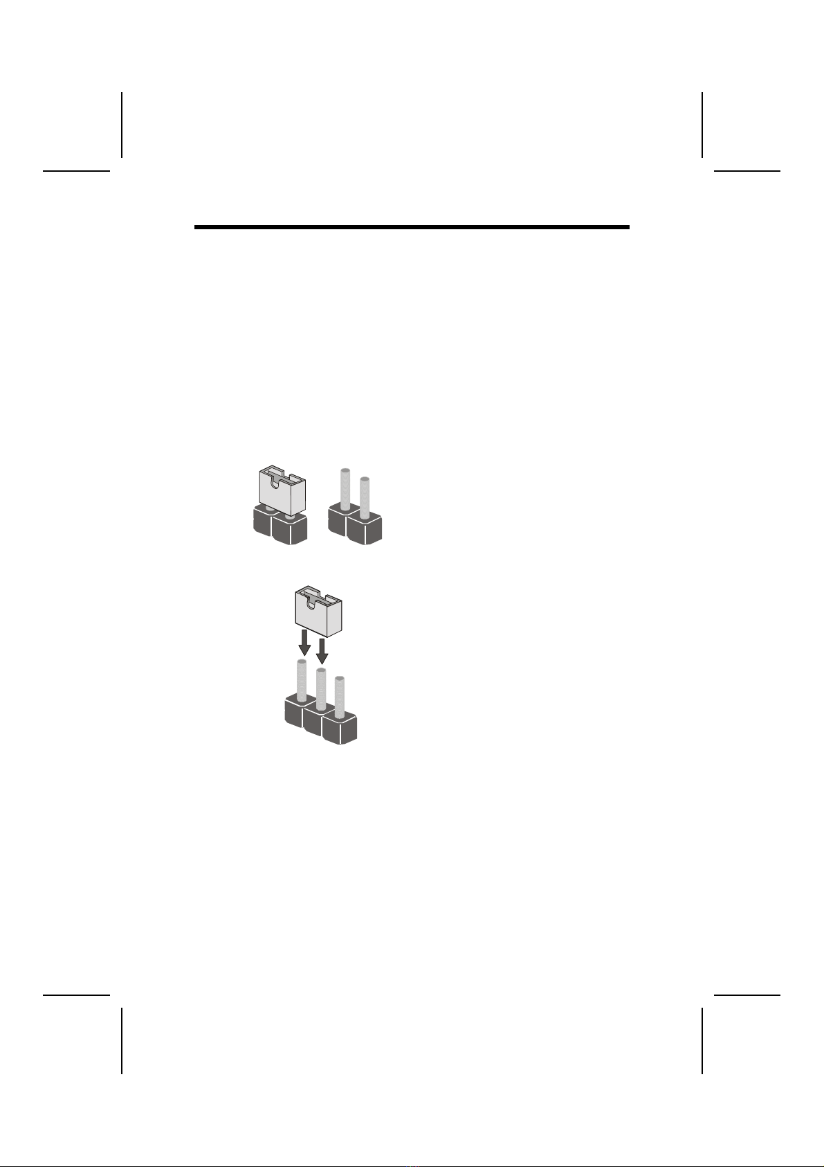
Setting Jumpers
Use the mainboard jumpers to set system configuration op-
tions. Jumpers with more than one pin are numbered. When
setting the jumpers, ensure that the jumper caps are placed
on the correct pins.
Short Open
This illustration shows a 2-pin
jumper. When the jumper cap is
placed on both pins, the jumper is
SHORT. If you remove the jumper
cap, or place the jumper cap on
just one pin, the jumper is OPEN.
123
This illustration shows a 3-pin
jumper. Pins 1 and 2 are SHORT.

10
Checking Jumper Settings
The following illustration shows the location of the mainboard
jumpers. Pin 1 is labeled.

11
Jumper Settings
Jumper Description Setting (default)
JBAT1 Clear CMOS
jumper
1-2: Normal
2-3: Clear CMOS
JBAT1
1
JP1A1 CPU Clock Short 1-2: 100M
Open 2-3: 133M
JP1A1
1
JP1B1 CPU Clock Short 2-3: 100M
Open 1-2: 133M
JP1B1
1
JP1 DRAM Volt-
age
Short 1-2: 3.3V
Open 1-2: 2.5V
JP1
J2A
J2B
J2C
J2D
DDR/SDR
DRAM Type
Selector
Short all J2A/B/C/D:
DDR1, DDR2
Open all J2A/B/C/D:
DIMM1, DIMM2
J2A/B/C/D
J3A
J3B
J3C
J4D
DDR/SDR
DRAM Type
Selector
Short all J3A/B/C/D:
DDR1, DDR2
Open all J3A/B/C/D:
DIMM1, DIMM2
J3A/B/C/D

12
JP2 Wake on
Keyboard/
USB activity
1-2: 5V
2-3: 5VSB
JP2
1
JP3 Flash ROM
Voltage
(VCC)
1-2: 5V
2-3: 3.3V
JP3
1
JP4 Flash ROM
Size
1-2: 2M
2-3: 4M
JP4
1
JBAT1: Clear CMOS Jumper
Use this jumper to clear the contents of the CMOS memory.
You may need to clear the CMOS memory if the settings in
the Setup Utility are incorrect and prevent your mainboard
from operating. To clear the CMOS memory, disconnect all the
power cables from the mainboard and then move the jumper
cap into the CLEAR setting for a few seconds.
JP1: DRAM Voltage (VCC)
This jumper enables to select voltage of DRAM.
JP1A1: CPU Clock
This jumper enables to select CPU frequency.
JP1B1: CPU Clock
This jumper enables to select CPU frequency.
J2A/J2B/J2C/J2D: DDR/SDR DRAM Type Selec-
tor
This jumper enables to select the type of DDR or SDR DRAM.
J3A/J3B/J3C/J3D: DDR/SDR DRAM Type Selec-
tor
This jumper enables to select the type of DDR or SDR DRAM.
JP2: Wake on Keyboard/USB activity
This jumper enables any USB keyboard activity to power up a
system previously in a standby or sleep state.

13
JP3: Flash ROM Voltage (VCC)
This jumper enables to select voltage for Flash ROM.
JP4: Flash ROM Size
This jumper enables to select size for Flash ROM.
14
I
In
ns
st
ta
al
ll
li
in
ng
g
t
th
he
e
M
Ma
ai
in
nb
bo
oa
ar
rd
d
i
in
n
a
a
C
Ca
as
se
e
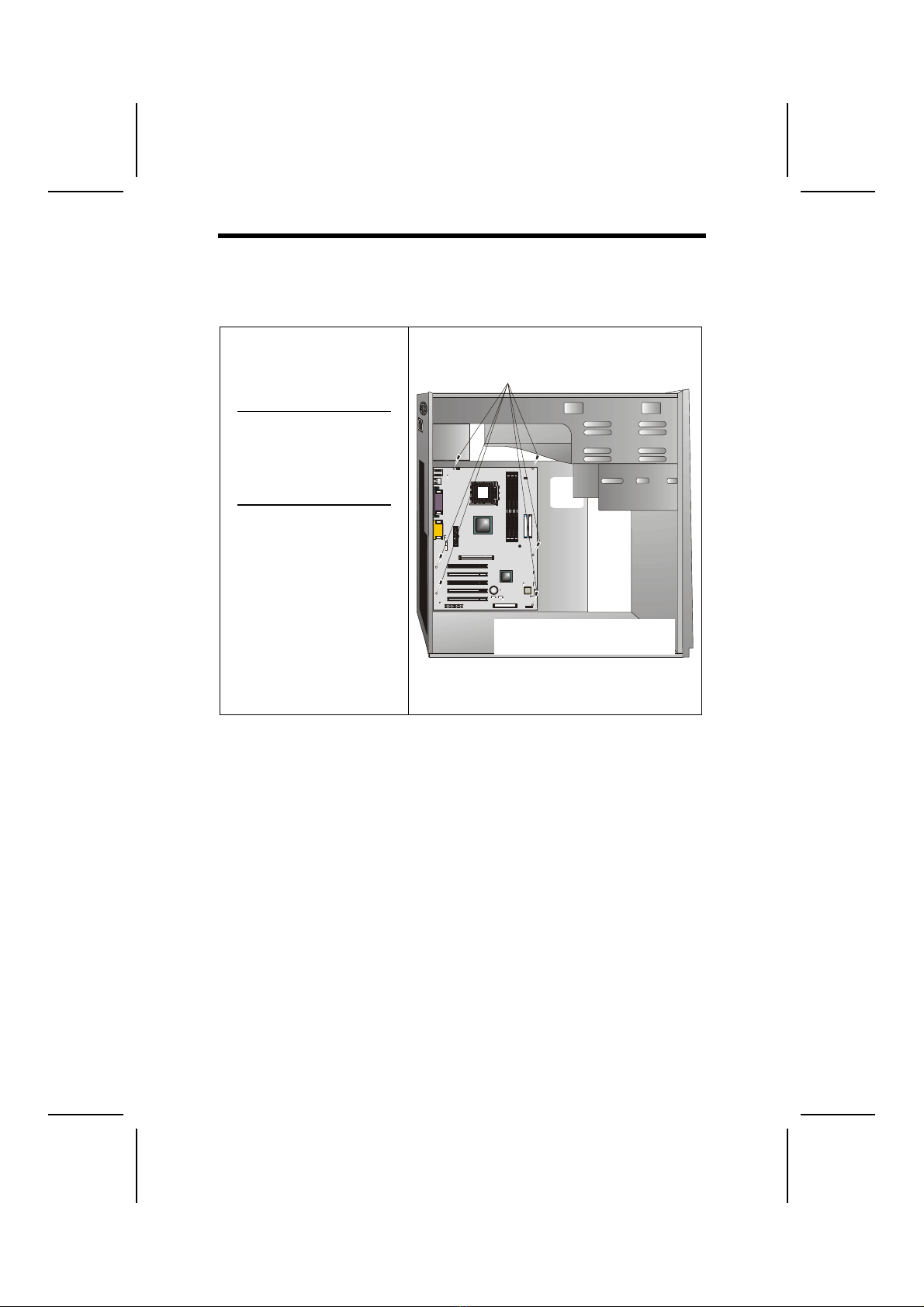
Refer to the following illustration and instructions for installing
the mainboard in a case:
This illustration shows
an example of a main-
board being installed in
a tower-type case:
Note: Do not over-
tighten the
screws as this
can stress the
mainboard.
Most system cases have
mounting brackets in-
stalled in the case,
which correspond to the
holes in the mainboard.
Place the mainboard
over the mounting
brackets and secure the
mainboard onto the
mounting brackets with
screws.
2. Secure the mainboard with
screws where appropriate.
1. Place the mainboard
over the mounting brackets.
Ensure that your case has an I/O template that supports the
I/O ports and expansion slots on your mainboard.
Table of contents
Other ECS Motherboard manuals


