ECS UM4980 User manual

.
.n
Y
EPA
POUUllON
PREVENTER
UM4980

-
-._-
40-012-42311/1,
Version 1.1
’
-
,’
Made in Taiwan

UM4980
User’s Manual

Trademarks
All brand and product names used in this manual may be trademarks or reg-
istered trademarks of their respective companies.

W
Table of Contents
Introduction
General Specifications
. . . . . . . . . . . . . . . . . . . . . . . . . . . . . . . . . . . . . . . . . . . . . . . . . . . . . .
1
System Memory
Memory Configurations
. . . . . . . . . . . . . . ..*...................................
3
Cache Memory Subsystem
. . . . . . . . . . . . . . . . . . . . . . . . . . . . . . . . . . . . . . . . . . . . . . . . .
5
Jumper Settings and Connectors
Setting the Jumpers
. . . . . . . . . . . . . . . . . . . . . . . . . . . . . . . . . . . . . . . . . . . . . . . . . . . . . . . . . .
6
Connectors
. . . . . . . . . . . . . . . . . . . . . . . . . . . . . . . . . . . . . . . . . . . . . . . . . . . . . . . . . . . . . . . . . . . .
9
Board Layout
. . . . . . . . . . . . . . . . . . . . . . . . . . . . . ..*.................................
10
Graphic Descriptions of Jumper Settings
. . . . . . . . . . . . . . . . . . . . . . . . . . . . . . . .
11
Built-in BIOS Setup Program
Setup Program
. . . . . . . . . . . . . . . . . . . . . . . . . . . . . . . . . . . . . . . . . . . . . . . . . . . . . . . . . . . . . . . .
23
System Setup
. . . . . . . . . . . . . . . . . . . . . . . . . . . . . . . . . . . . . . . . . . . . . . . . . . . . . . . . . . . . . . . . .
25
Fixed Disk Setup
. . . . . . . . . . . . . . . . . . . . . . . . . . . . . . . . . . . . . . . . . . . . . . . . . . . . . . . . . . . . .
26
Advanced System Setup
. . . . . . . . . . . . . . . . . . . . . . . . . . . . . . . . . . . . . . . . . . . . . . . . . . . .
28
Boot Options
. . . . . . . . . . . . . . . . . . . . . . . . . . . . . . . . . . . . . . . . . . . . . . . . . . . . . . . . . . . . . . . . . .
33
Security
. . . . . . . . . . . . . . . . . . . . . . . . . . . . . . . . . . . . . . . . . . . . . . . . . . . . . . . . . ..*............
34
Green PC Features
. . . . . . . . . . . . . . . . . . . . . . . . . . . . . . . . . . . . . . . . . . . . . . . . . . . . . . . . . .
35
Load ROM Default Values
. . . . . . . . . . . . . . . . . . . . . . . . . . . . . . . . . . . . . . . . . . . . . . . . .
38
Load Values from CMOS
. . . . . . . . . . . . . . . . . . . . . . . . . . . . . . . . . . . . . . . . . . . . . ...*.
39
Save Values to CMOS
. . . . . . . . . . . . . . . . . . . . . . . . . . . . . . . . . . . . . . . . . . . . . . . . . . . . . .
40
Quitting Setup
. . . . . . . . . . . . . . . . . . . . . . . . . . . . . . . . . . . . . . . . . . . . . . . . . . . . . . . . . . . . . . . .
41
Appendix A Setting the System Speed

1 Introduction
The UM4980 is a high performance 80486 VL-Bus mainboard which in-
cludes
UM8498F
and
UM8496F
chipsets. It also supports high integration
&
high performance solution.
1 .l General Specifications
Processor:
Chipset:
System BIOS:
Keyboard BIOS:
System Memory:
Cache Memory:
Slots
:
Connectors:
Form Factor:
Intel 80486
SX/SX2,
80487SX,
80486DX/DX2/DX4,
P24D
Cyrix Cx486S (M6), Cx486DXIDX2 (M7)
AMD
Am486DX/DX2,
Am486DXL/DXL2
UMC Green CPU
U5S-SUPER
UMC 8498F, UMC 8496F
Phoenix
AMI
KEYII
DRAM = >72 pins SIMM single or double density
EPRdM=>27C512
12812561512 KB, 1 MB
Seven (7) 16-bit AT slots
One
(I)
8-bit XT slot
Three (3) VL-Bus slots
Standard Power Connector
Hard ware Reset Connector
Ext Speaker Connector
External Battery
Turbo Switch
Suspend/Resume Push Botton
Turbo LED
Keylock Connector, Power LED
Keyboard Connector
4 layers, 2/3 Baby-AT

UM4980
User’s
Manual
Features
l
100% IBM PC/AT compatible
l
Supports Local Bus Access
l
Supports H/W and S/W Turbo Control
l
Provides Fast CPU Reset and Fast Gate 20
l
Built-in direct map write through
&
write back cache controller
l
Flexible cache memory size
128/256/512
KB/lMB
l
Supports four banks memory up to 64MB
l
Supports double density for bank2 and bank3
l
Supports 64MB addressing space for DMA
l
Seven AT Bus slots including three VESA master slots
l
Performs zero wait burst read for the 486 CPU
l
Programmable DRAM Access wait state O/l
/2
l
One
237/238
ZIF pins CPU socket which supports
486SX/SX2/DX/DX2/DX4,
AMD486/M6/M7/P24D/U5
UM4980
User’s Manual
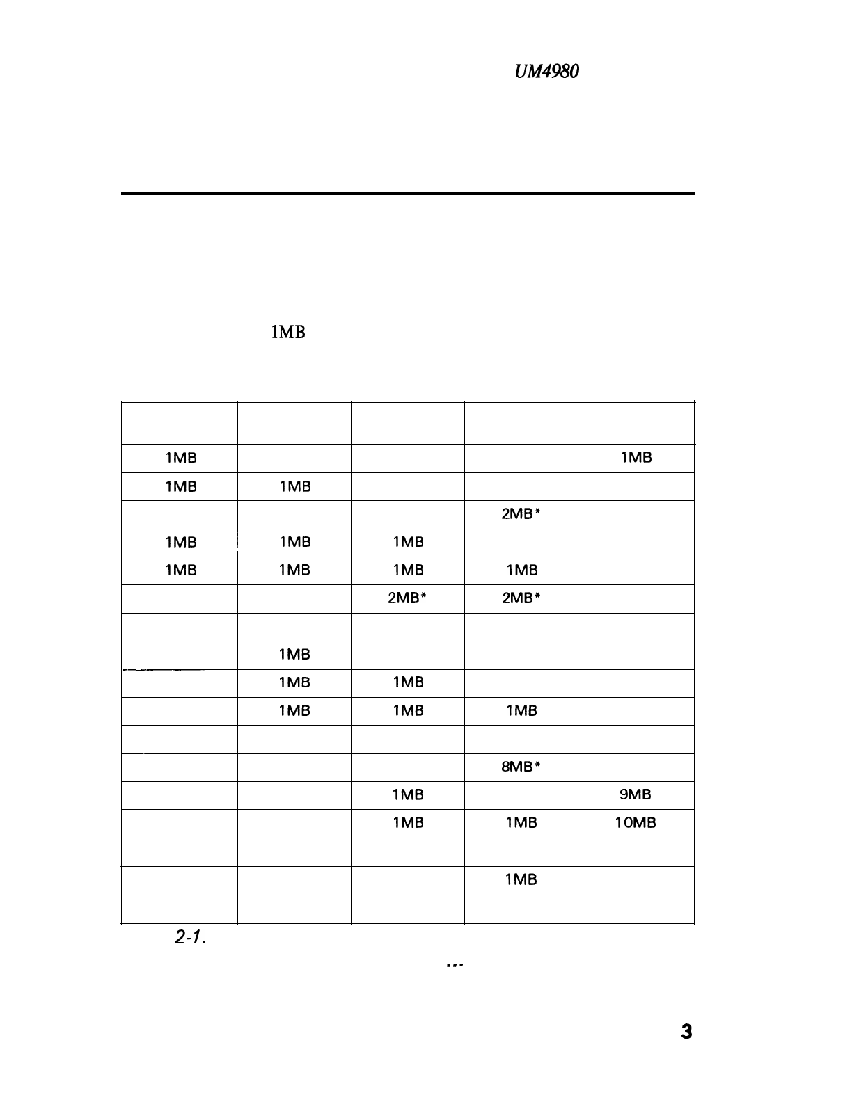
2 System Memory
2.1 Memory
Configurations
The UM4980
provides tremendous flexibility to support a number of differ-
ent on-board DRAM configurations. The on-board DRAM is installed with
Single-In-Line Memory Module (SIMM). There are four memory banks ca-
pable of supporting
1MB
up to 64MB.
The following table lists all the possible DRAM module combinations and
the total memory amount for each option.
SIMM 1
SIMM 2 SIMM 3
SIMM4
Tot
al
Memory Size
IMB
IMB
IMB
IMB
2MB
2MB” 2MB
IMB
,
I
IMB IMB
3MB
IMB
IMB IMB IMB
4MB
2MB” 2MB” 4MB
4MB 4MB
4MB
IMB
5MB
--______
4MB
IMB
1MB
6MB
4MB
1MB
IMB IMB
7MB
4MB 4MB 8MB
-
8MB” 8MB
4MB 4MB
IMB
9MB
4MB 4MB
IMB
1MB
IOMB
4MB 4MB 4MB 12MB
4MB 4MB 4MB
IMB
13MB
4MB 4MB 4MB 4MB 16MB
Table
2-
1.
Memory Bank Configurations and Requirements
Continued..
...
3

UM4980
User's
Manud
SIMM 1 SIMM 2 SIMM 3 SIMM 4
Total
Memory Size
8MB” 8MB” 16MB
16MB 16MB
16MB
/
1MB
17MB
16MB
1MB
IMB
’
18MB
16MB
1MB
IMB
IMB
19MB
16MB 4MB 20MB
16MB
1
4MB
IMB
1
21MB
16MB 4MB
IMB
IMB
22MB
16MB 4MB 4MB 24MB
16MB 4MB 4MB
IMB
25MB
16MB 4MB 4MB 4MB 28MB
16MB 16MB 32MB
16MB 16MB
IMB
33MB
16MB
I
16MB
I
IMB
I
IMB
I
34MB
16MB 16MB 4MB
/
36MB
16MB 16MB 4MB
1
1MB
37MB
16MB 16MB 4MB 4MB 40MB
16MB
I
16MB
I
16MB
I
I
48MB
16MB
j
16MB
I
16MB
I
IMB
I
49MB
16MB
j
16MB
j
16MB
1
4MB
/
52MB
16MB 16MB 16MB 16MB 64MB
*: It means double density.
Table
2-
1.
Memory Bank Configurations and Requirements
(Continued.
.
.
.
.
I
4
UM4980
User’s
Munuul
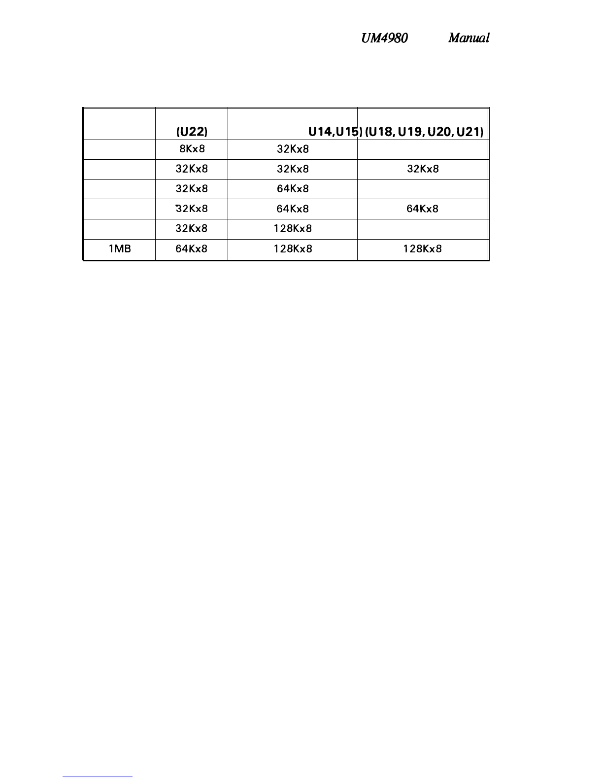
2.2 Cache Memory Configuration
Option
TAG RAM Cache Bank0
Cache Bank 1
NJ221
(U12, U13,
U14,U15)
(U18, U19, U20, U21)
128K 8Kx8
32Kx8
None
256K
32Kx8 32Kx8 32Kx8
256K
32Kx8 64Kx8
None
512K
32Kx8 64Kx8 64Kx8
512K
32Kx8 128Kx8
None
1MB
64Kx8 128Kx8 128Kx8
Table 2-2. Secondary Cache Memory Configurations
5
UM4980
User's
Manual
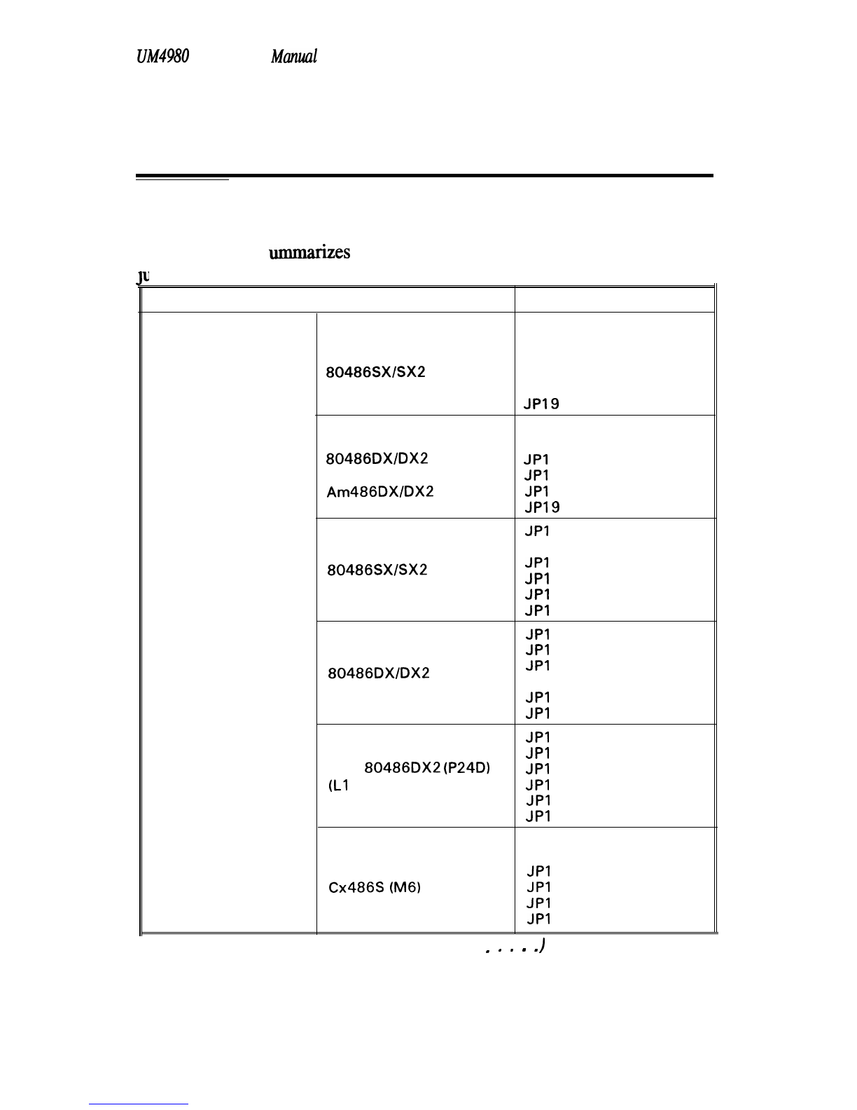
3 Jumper Settings and Connectors
3.1 Setting the Jumpers
The table below s
ummarizes the appropriate functions and settings of each
jumper on theUM4980.
CPU Type
Function
Intel
80486SXISX2
Intel
80486DX/DX2
AMD
Am486DX/DX2
Intel
80486SX/SX2
(SL Enhance)
Intel
80486DX/DX2
(SL Enhance)
Intel
80486DX2
(P24D)
(Ll
Write-Back)
Cyrix
Cx486S
(M6)
Jumper Settings
JP14 open
JP15 short 2-3
JP16 open
JP17 open
JP18 short 2-3
JPl9
open
JP14 open
JP15 short l-2, 3-4
JPI
6 short l-2
JPI
7 open
JPI
8 short 2-3
JP19
open
JPI
4 short 1-2, 3-4
JP15 short 2-3
JPI
6 open
JPI
7 short 5-6
JPI
8 short 1-2
JPI
9 short 1-2
JPI
4 short l-2, 3-4
JPI
5 short l-2, 3-4
JPI
6 short l-2
JP17 short 5-6
JPI
8 short l-2
JPI
9 short 1-2
JPI
4 short l-2, 3-4
JPI
5 short l-2, 3-4
JPI
6 short l-2
JPI
7 short 3-4, 5-6
JPI
8 short l-2, 4-5
JPI
9 short l-2, 4-5
JP14 short 2-3, 4-5
JP15 short 2-3
JPI
6 open
JPI
7 short 2-3, 4-5
JPI
8 short l-2, 3-4, 5-6
JPI
9 short l-2, 3-4, 5-6
Table
3-7
.
Jumper Settings (Continued
..
.
.
.
)
6
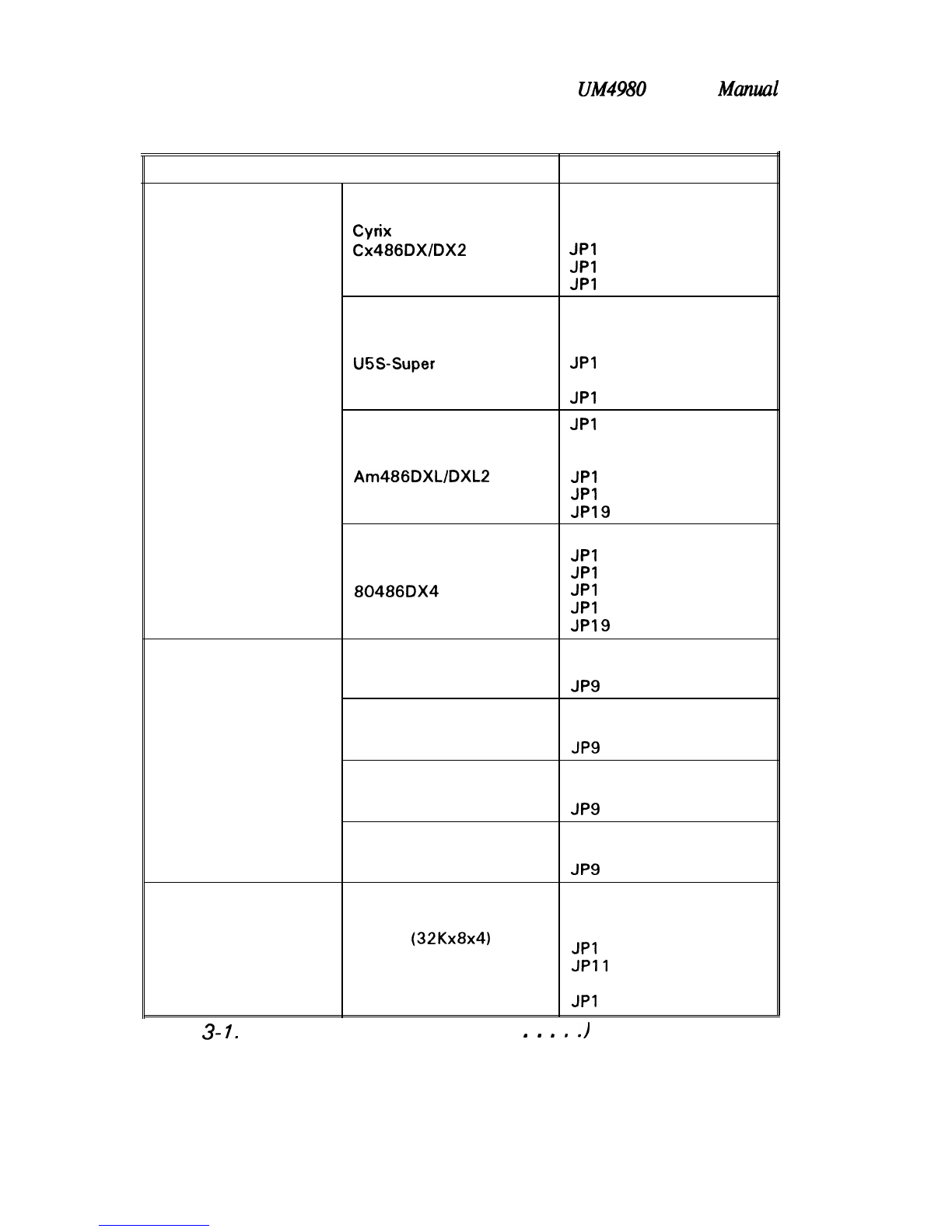
UM4980
User’s
Manual
CPU Type
Function
cyrix
Cx486DX/DX2
UMC Green CPU
UFiS-Super
AMD
Am486DXL/DXL2
Jumper Settings
JP14 short 2-3
JP15 short l-2, 3-4
JP16 short l-2
JPI
7 short 2-3, 4-5
JPI
8 short 1-2, 3-4, 5-6
JPI
9 short 1-2, 3-4
JP14 open
JP15 short 2-3
JP16 short 3-4
JPI
7 short 1-2
JP18 short 2-3
JPI
9 short 2-3
JPI
4 open
JP15 short l-2, 3-4
JP16 short l-2, 3-4
JPI
7 short l-2
JPI
8 short 2-3
JP19 short 2-3
Intel
804860X4
JP14 short l-2, 3-4
JPI
5 short 1-2, 3-4
JPI
6 short l-2
JPI
7 short 5-6
JPI
8 short 1-2
JP19 short 1-2
Clock Select
25 MHz
33 MHz
40 MHz
50 MHz
JP7 short
JP8 open
JP9 open
JP7 short
JP8 short
JP9 short
JP7 short
JP8 short
JP9 open
JP7 open
JP8 open
JP9 short
JP4 short 1-2
JP5 short l-2
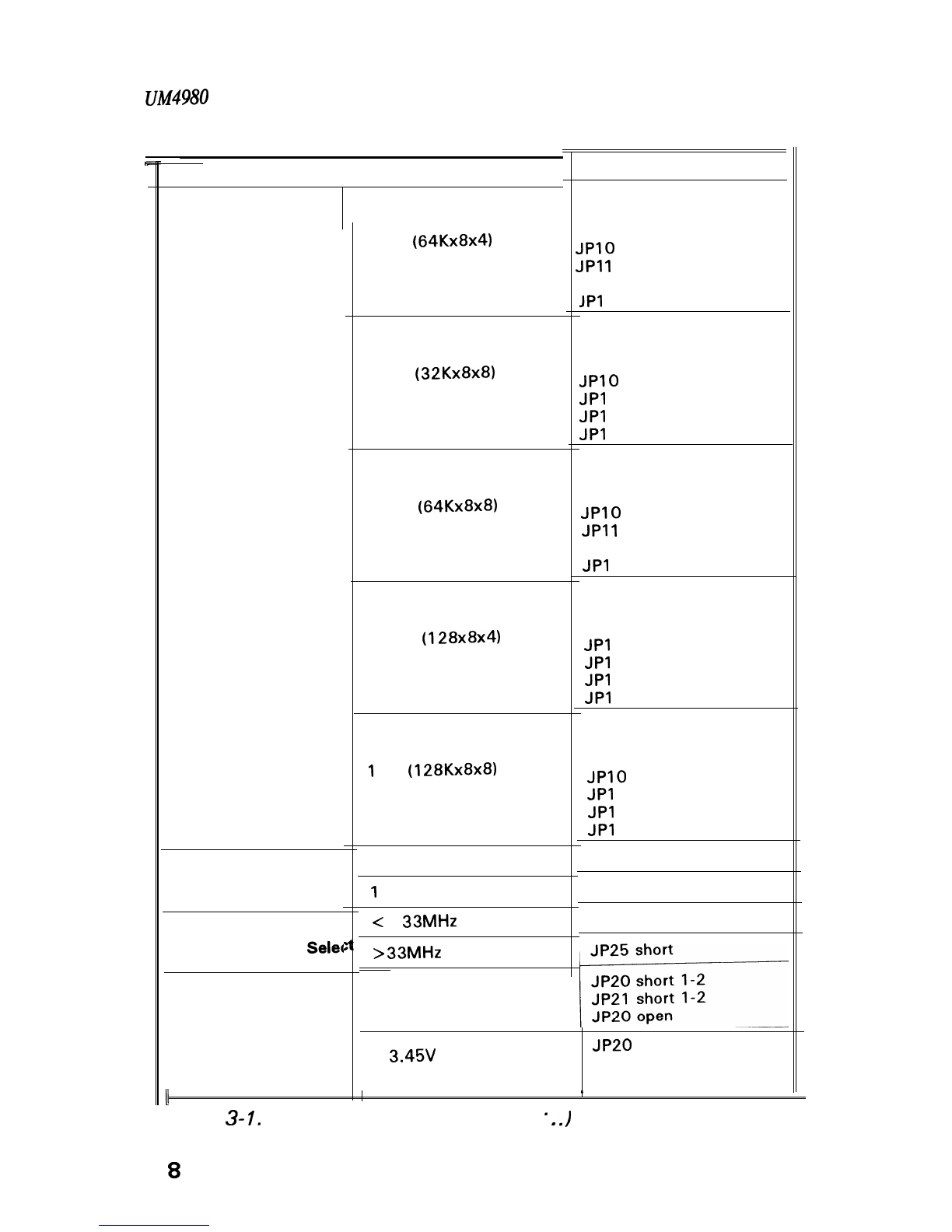
128KB (32Kx8x4)
JP6 open
Cache Memory Settings (one bank) JPI
0 open
JPll
open
JP12 open
JPI
3
open
Table
3-
7.
Jumper Settings (Continued
...,
.)
7
UM4980
User's
Manual
Function
Cache Memory Set-
tings
Local Bus Write Wait
Select
Local Bus Speed
Selec
CPU Voltage
256KB
(64Kx8x4)
[one bank)
256KB
(32Kx8x8)
(two bank)
512KB
(64Kx8x8)
(two bank)
5 12KB
(128x8~4)
(one bank)
II
I
Table 3-
I.
Jumper Settings (Continued..
.
.
.)
1
MB
(I
28Kx8x8)
(two bank)
0 Wait State
I
Wait State
<
=
33MHz
>
33MHz
+ 5V (Source from
standard power supply
unit)
Jumper Settings
JP4 short l-2
JP5 short l-2
JP6 short l-2
JPIO
open
JPI
I
open
JP12 open
JPI 3 short
JP4 short 2-3
JP5 short 2-3
JP6 open
JPIO
open
JPI
1 open
JPI
2 open
JPI
3 short
JP4 short 2-3
JP5 short 2-3
JP6 short 2-3
JPIO
open
JPI
I
short
JP12 open
JPI
3 short
JP4 short l-2
JP5 short 2-3
JP6 short 2-3
JPI
0 short l-2
JPI
1 short
JPI
2 open
JPI
3 short
JP4 short 2-3
JP5 short 2-3
JP6 short 2-3
JPIO
short 2-3
JPI
1 short
JPI
2 short
JPI
3 short
JP26 open
JP26 short
JP25 open
+
3.45V
(Source from on
JP20
short 2-3
board regulator) JP21 short 2-3
JP22 short l-2
8

VM4980
User’s
Manual
Function
I
Jumper Settings
II
CPU Voltage +
3.3V
(Source from on
board regulator)
JP20
short 2-3
JP21 short 2-3
JP22 short 2-3
Flash ROM
only when programming
a + 5V flash ROM
JPl
short 3-2
only when programming
a +
12V
flash ROM
JPI
short 2-3
Normal EPROM
JPl
open
II
Note:
JP24: Opens for
DX4
Internal CLK 3X
Shorts for DX4 Internal CL K 2X
(2-3).
JP3:
Opens for external keyboard control
Shorts for in
ternal
keyboard control.
3.2 Connectors
There are several connectors located on the
UM4980.
They are used to con-
nect with some peripheral devices to enhance the operating performance of
the system. Refer to Figure 3.1 for the positions of all the connectors on the
mainboard. The following table lists the connectors on the
UM4980.
Connector Function
Jl
Power Supply Connector
J2 External Battery Connector
-
J3 Keyboard Connector
J27 Suspend/Resume (Push Botton)
J28 Turbo LED
J29 External Speaker Connector
J30
Hard ware Reset Connector
J31
Turbo Switch
J32 Keyboard Lock/Power LED
Table 3-2. Mainboard Connectors
Note:
You can only push the J27 button to enter suspend/re-
sume modes when the system is in
‘YDLE”
state other-
wise the system will halt or your data may be
destroyed.

UM4980
User's
Manual
3.3 Board Layout
Keyboard Connector
VL-Bus
Slots
!L!L
j$j
JP25
JP26
Expansion
Slots
JPl
J32
J31J30
J29
JP9mJP7
JP6
l-----r
CPU
Jl
I
wij--
Power
I
L
1
S
I
I
M
2
Connector
B
r’l
I
0
S
r
S
I
M
1
Key(ock
I
Reset
Turbo
\
Turbo
\
LED Suspend
swltdl
Spe8ker Resume
Figure 3-1.
UM4980
Mainboard Layout
IO

UM4980
User’s Mmuul
3.4
Graphical Descriptions of Jumper Settings
p-G+
signifies ins 1 & 2 are set as “short.”
pB-i!j
means that this jumer is set as “open.”
CPU Type
1.
Intel
80486SX/SX2
CPU installed on-board
\
r
.
CPU
Socket
\
JP15
11

UM4980
User’s Manual
2. Intel
80486DX/DX2/Am486DX/DX2
CPU installed on-board
CPU
Socket
\
LiII
UM8498F
JP15
1
88
01
JPl6;
g
JP’4
m
8
4 O
3.
Intel
80486SX/SX2
(SL
Enhance) CPU installed on-board
1
UM8496F
1
JP15
12

UM4980
User'sibzuul
4.
80486 DX/DX2 (SL Enhance) CPU installed on-board
!1
UM8496F
El
UM8498F
r
I-
CPU
Socket
JP15
1
JP14
5. Intel 80486 DX2
(Ll
Write-Back,
P24D)
CPU installed on-board
El
UM8496F
,
JP15
CPU
I
Socket
-
13

UM4980
Vser's_Mmual
6. Cyrix Cx
486s
(M6) CPU installed on-board
-
El
UM8496F
1
UM8498F
J
CPU
Socket
JP17
8
7. Cyrix
Cx486DX/DX2
CPU installed on-board
UM8498F
CPU
Socket
JP15
1
JPl JP17
6
JPl%
14

UM4980
User'sManuul
8. UMC Green CPU
U5S-Super
CPU installed on-board
El
UM8496F
1
UM8498F
CPU
Socket
5
1
JPl JP17
6
JP18
I
9.
AM0
Am486 DXL/DXL2 CPU installed on-board
CPU
Socket
15
Table of contents
Other ECS Motherboard manuals


