Epson S5U1C17965T2 User manual

Rev.1.0
CMOS 16-BIT SINGLE CHIP MICROCONTROLLER
S5U1C17965T2 Manual
(Software Evaluation Tool for S1C17555/565/955/965)

Evaluation board/kit and Development tool important notice
1. This evaluation board/kit or development tool is designed for use for engineering evaluation, demonstration,
or development purposes only. Do not use it for other purposes. It is not intended to meet the requirements of
design for finished products.
2. This evaluation board/kit or development tool is intended for use by an electronics engineer and is not a
consumer product. The user should use it properly and in a safe manner. Seiko Epson dose not assume any
responsibility or liability of any kind of damage and/or fire coursed by the use of it. The user should cease to
use it when any abnormal issue occurs even during proper and safe use.
3. The part used for this evaluation board/kit or development tool may be changed without any notice.
NOTICE
No part of this material may be reproduced or duplicated in any form or by any means without the written
permission of Seiko Epson. Seiko Epson reserves the right to make changes to this material without notice.
Seiko Epson does not assume any liability of any kind arising out of any inaccuracies contained in this material
or due to its application or use in any product or circuit and, further, there is no representation that this material is
applicable to products requiring high level reliability, such as, medical products. Moreover, no license to any
intellectual property rights is granted by implication or otherwise, and there is no representation or warranty that
anything made in accordance with this material will be free from any patent or copyright infringement of a third
party. When exporting the products or technology described in this material, you should comply with the
applicable export control laws and regulations and follow the procedures required by such laws and regulations.
You are requested not to use, to resell, to export and/or to otherwise dispose of the products (and any technical
information furnished, if any) for the development and/or manufacture of weapon of mass destruction or for other
military purposes.
All brands or product names mentioned herein are trademarks and/or registered trademarks of their respective
companies.
©SEIKO EPSON CORPORATION 2014,All rights reserved.

Configuration of product number
Devices
S1
C
17xxx
F
00E1
00
Development tools
S5U1
C
17000
Y2
1
00
■Packing specifications
[00: standard packing]
■Version
[1: Version 1]
■Tool type
Hx: ICE
Tx: Evaluation board
Cx: Compiler package
Yx: Writer software
■Corresponding model number
[17xxx: for S1C17xxx]
■Tool classification
[C: microcomputer use]
■Product classification
[S5U1: development tool for semiconductor
products]
■Packing specifications
00: Besides tape & reel
0A: TCP BL 2 directions
0B: Tape & reel BACK
0C: TCP BR 2 directions
0D: TCP BT 2 directions
0E: TCP BD 2 directions
0F: Tape & reel FRONT
0G: TCP BT 4 directions
0H: TCP BD 4 directions
0J: TCP SL 2 directions
0K: TCP SR 2 directions
0L: Tape & reel LEFT
0M: TCP ST 2 directions
0N: TCP SD 2 directions
0P: TCP ST 4 directions
0Q: TCP SD 4 directions
0R: Tape & reel RIGHT
99: Specs not fixed
■Specification
■Package
[D: bare chip, F: QFP, B: BGA]
■Model number
■Model name
[C: microcomputer, digital products]
■Product classification
[S1: semiconductor]


S5U1C17965T2 Manual Seiko Epson Corporation i
(Rev.1.0)
Table of Contents
1. Overview..................................................................................................................... 1
1.1 Usage Method.............................................................................................................................1
2. Block Diagram............................................................................................................ 2
3. Hardware Information................................................................................................ 3
3.1 Layout Information.....................................................................................................................3
3.2 Jumper Information....................................................................................................................5
3.3 Circuit Diagram...........................................................................................................................6
3.4 Components List ........................................................................................................................8
Revision History............................................................................................................. 10


1. Overview
S5U1C17965T2 Manual Seiko Epson Corporation 1
(Rev.1.0)
1. Overview
The S5U1C17965T2 (Software Evaluation Tool for S1C17555/565/955/965) is an evaluation and development
support board for the Seiko Epson single-chip microcontroller S1C17555/565/955/965.
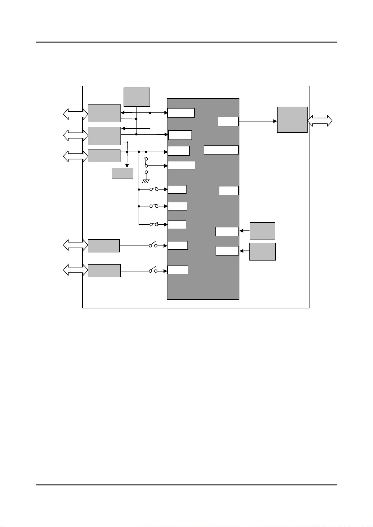
The S5U1C17965T2 has the S1C17965 chip and circuits for external connections, and provides through-holes for
extension connectors that draw out the S1C17965 I/O pins. By connecting this tool with a user board via these
through-holes, the functions of the tool can expanded.
The S5U1C17965T2 can be used as the S1C17555/565/955/965 software development environment, by
connecting to the Seiko Epson emulator S5U1C17001H (ICDmini).
- Operating temperature range 5°C to 35°C
- Operating voltage range (Please refer to the technical manual for S1C17555/565/955/965.)
1.1 Usage Method
The S1C17555/565/955/965 software development environment can be set up with the following procedures.
(1) Insert the S1C17965 chip into the IC socket (U1)*1.
(2) Connect*2 the S5U1C17001H (ICDmini) to the ICDmini interface connectors (J5, J6) using the dedicated
cables included in the ICDmini.
(3) Provide power supplies*3 through the power supply connectors (J8, J9, J10).
(4) Connect the ICDmini to a PC *4 using the USB cable included in the ICDmini.
*1 Insert the S1C17965 chip in the direction where the No.1 pin of the chip is matched to the position of ▼
(triangle) mark printed on the board. If the chip is inserted in a wrong direction and the power supply is
turned on, the chip might be damaged.
*2 For more information on connecting this product, refer to the S5U1C17001H User Manual (ICDmini
Ver2.0). Use the S5U1C17001H2 (ICDmini Ver2.0) or later versions for this product. When using with the
S5U1C17002H (ICD Board), make the Vpp regulator / boost circuit enabled with jumper settings. Refer to
Chapter 3 in details.
*3 DO NOT apply a voltage exceeding the S1C17965 power supply voltage input range. For the S1C17965
power supply voltage input range, refer to the S1C17555/565/955/965 Technical Manual. When using the
LVDD and AVDD regulators, the power supplies through J8 and J10 are unnecessary. Refer to Chapter 3 in
details.
*4 The software development tool S5U1C17001C (GNU17) should be installed in the PC that is used for the
S1C17555/565/955/965 development. Use the GNU17 Ver2.0.0 or later versions for this product.
Note: When using the S5U1C17965T2, use the spacers included in this product to prevent the mounted
components from being short-circuited.

2. Block Diagram
2 Seiko Epson Corporation S5U1C17965T2 Manual
(Rev.1.0)
2. Block Diagram
Figure 2.1 shows the S5U1C17965T2 block diagram.
Figure 2.1 S5U1C17965T2 block diagram
S1C17965
OSC1
32kHz
OSC3
12MHz
Reset
SW
Debug i/f
Through
Hole
External
Power (HVDD)
ICDmini
Connector
Connector
ICDmini
ICDboard
Connector
Target
Board
Connector
External
Power (LVDD)
ICDboard
LED
Connector
External
Power (AVDD)
VINL
REGEN
AVDD
MSIF
SIN/SOUT
HVDD
VINA
VINP
LVDD
Ports
OSC1
OSC3
RESET

3. Hardware Information
S5U1C17965T2 Manual Seiko Epson Corporation 3
(Rev.1.0)
Extension
Connector (J2)
(foot pattern only*1*2)
Reset SW
(SW1)
HVDD-IN
(J9)
LVDD-IN
(J8)
AVDD-IN
(J10)
Extension
Connector(J4)
(foot pattern
only
*1*2
)
Extension
Connector(J3)
(foot pattern only)*1*2
Extension
Connector (J1)
(foot pattern
only*1*2)
S1C17965
*3
(U1)
1 Pin
3. Hardware Information
3.1 Layout Information
The S5U1C17965T2 component layout is shown in Figure 3.1 and 3.2.
Figure 3.1 S5U1C17965T2 component layout (front side)
*1 The extension connectors J1, J2, J3 and J4 are provided with only foot patterns. The components included in
this product should be mounted on them , if necessary.
*2 The through-hole bore diameter is 0.85 mm.

3. Hardware Information
4 Seiko Epson Corporation S5U1C17965T2 Manual
(Rev.1.0)
Figure 3.2 S5U1C17965T2 component layout (rear surface)
ICDboard
i/f
Connector
(J7)
ICDmini i/f
Connector
(J5)
ICDmini i/f
Connector
(J6)
12MHz
Crystal Unit (X2)
32.768kHz
Crystal Unit (X1)

3. Hardware Information
S5U1C17965T2 Manual Seiko Epson Corporation 5
(Rev.1.0)
3.2 Jumper Information
Table 3.1 shows the S5U1C17965T2 jumper functions list.
Table 3.1 Jumper settings list
Description
Factory default setting
Selectable function
JP10
REGEN EN: CLOSE
(LVDD regulator: enabled)
REGEN DS: CLOSE
(LVDD regulator: disabled)
JP14 OPEN
(LVDD supply via J8: disabled)
CLOSE
(LVDD supply via J8: enabled)
JP16
CLOSE
(AVDD supply via J10: enabled)
CLOSE
(AVDD supply via J10: disabled)
JP18 CLOSE
(ICDmini supply via VPP: enabled)
OPEN
(ICDmini supply via VPP: disabled)
JP15
CLOSE
(LVDD regulator: enabled)
OPEN
(LVDD regulator disabled)
JP17 CLOSE
(AVDD regulator: enabled)
OPEN
(AVDD regulator: disabled)
JP19
CLOSE
(VPP regulator: enabled)
OPEN
(VPP regulator: disabled)
JP4 OPEN
(LVDD supply via J8: disabled)
CLOSE
(LVDD supply via J8:enabled)
JP5
CLOSE
(HVDD supply via J9: enabled)
OPEN
(HVDD supply via J9: disabled)
JP6 CLOSE
(AVDD supply via J10: enabled)
OPEN
(AVDD supply via J10: disabled)
JP1,JP2,JP3,J
P7,JP8,JP9,JP
11,JP12,JP13
CLOSE (Solder Bridge)
-

3. Hardware Information
6 Seiko Epson Corporation S5U1C17965T2 Manual
(Rev.1.0)
3.3 Circuit Diagram
Figure 3.3 S5U1C17965T2 circuit diagram (1)

3. Hardware Information
S5U1C17965T2 Manual Seiko Epson Corporation 7
(Rev.1.0)
Figure 3.3 S5U1C17965T2 circuit diagram (2)

3. Hardware Information
8 Seiko Epson Corporation S5U1C17965T2 Manual
(Rev.1.0)
3.4 Components List
Table 3.2 S5U1C17965T2 components list *1
Description
Location
Model no. / specifications
Qty.
Manufacturer
MCU U1
S1C17965F
(TQFP13-64)
1 SEIKO EPSON CORPORATION
IC socket
(U1)
IC51-0644-807-6
1
YAMAICHI electronics
Crystal oscillator
X1
MC-146 (7pF)32.768kHz
1
SEIKO EPSON CORPORATION
Crystal oscillator X2
FA-238V 12MHz
(10pF ±50ppm)
1 SEIKO EPSON CORPORATION
Voltage detection IC
U3
S-1000N15-N4T1G
1
Seiko Instruments Inc.
General purpose
logic
U2 SN74LVC1G97DCK 1 Texas Instruments
U4
AH6100LR
0
(Unmounted)
USB to UART
Bridge
U5 CP2102-GM 0 SILICON LABS (Unmounted)
LED
D1
PG1111C
1
STANLAY ELECTRIC CO., LTD.
Diode
D2
CRS06
1
TOSHIBA
Diode
D3,D4,D5
1N5819
0
ON Semiconductor (Unmounted)
Switch
SW1
SKRAAKE010
1
ALPS ELECTRIC CO., LTD.
Connector
J5
A2-4PA-2.54DS(71)
1
HIROSE ELECTRIC
CO., LTD.
Connector
J6
S04B-PASK-2(LF)(SN)
1
JST Mfg. Co., Ltd
Connector
J7
PS-10SD-D4T1-1
1
Japan Aviation Electronics
Connector
J11
54819-0572
0
Molex (Unmounted)
Connector
J8,J9,J10
S2B-XH-A(LF)(SN)
3
JST Mfg. Co., Ltd
Jumper pin
JP4,JP5,JP6,
JP14,JP15,
JP16,JP17,
JP18,JP19
WL-1-2P 9 Mac-Eight Co.,Ltd.
Jumper pin
JP10
WL-1-3P
1
Mac-Eight Co.,Ltd.
Jumper socket
JP4,JP5,JP6,
JP10,JP14,
JP15.JP16,
JP17,JP18,
JP19
JS-1 10 Mac-Eight Co.,Ltd.
Chip ceramic
capacitor
C31,C32,C33,
C34,C35,C36,
C37,C38,C39
0.022µF/16V 0 (Unmounted)
C27,C28,C29,
C30
0.1µF/16V 0 (Unmounted)
C49
1µF/16V
0
(Unmounted)
C26
10µF/16V
0
(Unmounted)
Chip ceramic
capacitor
C14,C15
C1608CH1H010C
10pF/16V
2 TDK Corporation
C20,C21
C1608JB1E224K
0.22µF/16V
2 TDK Corporation
C2,C4,C6,C8,
C9,C10,C11,
C13,C18,C19,
C22,C23,C25,
C40,C42,C44,
C46,C47,C48,
C53
C1608JB1E104K
0.1µF/16V 20 TDK Corporation
C1,C3,C5,C7,
C12,C24,C41,
C43,C45,C52
C2012Y5V1C106Z
10µF/16V 10 TDK Corporation
C16,17
0
(Unmounted)

3. Hardware Information
S5U1C17965T2 Manual Seiko Epson Corporation 9
(Rev.1.0)
Description
Location
Model no. / specifications
Qty.
Manufacturer
Chip resistor
R1,R19,R20
0Ω/0.1W
0
(Unmounted)
R17
4.7kΩ/0.1W
0
(Unmounted)
R9,R10,R11,
R12,R13,R14
33kΩ/0.1W 0 (Unmounted)
Chip resistor
R5,R8,R15
RK73Z2AT 0Ω/0.1W
3
KOA Corporation
R18
RK73H2ATTD33R0F
33Ω/0.1W
1 KOA Corporation
R3 RK73H2ATTD6800F
680Ω/0.1W
1 KOA Corporation
R2
RK73H2ATTD1002F
10kΩ/0.1W
1 KOA Corporation
R7 RK73H2ATTD4702F
47kΩ/0.1W
1 KOA Corporation
R16
RK73H2ATTD4703F
470kΩ/0.1W
1 KOA Corporation
R6 RK73H2ATTD1004F
1MΩ/0.1W
1 KOA Corporation
R4
RK73H2ATTD1005F
10MΩ/0.1W
1 KOA Corporation
Power cable
(housing)
Accessories XHP-2 3 JST Mfg. Co., Ltd
Power cable
(contact)
Accessories BXH-001T-P0.6 6 JST Mfg. Co., Ltd
Power cable (wire) Accessories AWM1007/TR-64 6 SHINAGAWA ELECTRIC WIRE
CO.,LTD
Spacer
Accessories
BSB-308E
4
Hirosugi-Keiki Co., Ltd
Screw
Accessories
FB-0306N
4
Wilco
Connector Accessories
(can be mounted
on J1, J2, J3, J4) FFC-40BMEP1B 4 Honda Tsushin Kogyo Co., Ltd.
*1 The components listed above are subject to change without notice.

Revision History
10 Seiko Epson Corporation S5U1C17965T2 Manual
(Rev.1.0)
Revision History
Attachment-1
Rev. No.
Date
Page
Category
Contents
Rev 1.0
2014/07/31
All
new

International Sales Operations
AMERICA
EPSON ELECTRONICS AMERICA, INC.
214 Devcon Drive,
San Jose, CA 95112, USA
Phone: +1-800-228-3964 FAX: +1-408-922-0238
EUROPE
EPSON EUROPE ELECTRONICS GmbH
Riesstrasse 15, 80992 Munich,
GERMANY
Phone: +49-89-14005-0 FAX: +49-89-14005-110
ASIA
EPSON (CHINA) CO., LTD.
7F, Jinbao Bldg., No.89 Jinbao St.,
Dongcheng District,
Beijing 100005, CHINA
Phone: +86-10-8522-1199 FAX: +86-10-8522-1125
SHANGHAI BRANCH
7F, Block B, Hi-Tech Bldg., 900 Yishan Road,
Shanghai 200233, CHINA
Phone: +86-21-5423-5577 FAX: +86-21-5423-4677
SHENZHEN BRANCH
12F, Dawning Mansion, Keji South 12th Road,
Hi-Tech Park, Shenzhen 518057, CHINA
Phone: +86-755-2699-3828 FAX: +86-755-2699-3838
EPSON HONG KONG LTD.
Unit 715-723, 7/F Trade Square, 681 Cheung Sha Wan Road,
Kowloon, Hong Kong.
Phone: +852-2585-4600 FAX: +852-2827-4346
EPSON TAIWAN TECHNOLOGY & TRADING LTD.
14F, No. 7, Song Ren Road,
Taipei 110, TAIWAN
Phone: +886-2-8786-6688 FAX: +886-2-8786-6660
EPSON SINGAPORE PTE., LTD.
1 HarbourFront Place,
#03-02 HarbourFront Tower One, Singapore 098633
Phone: +65-6586-5500 FAX: +65-6271-3182
SEIKO EPSON CORP.
KOREA OFFICE
5F, KLI 63 Bldg., 60 Yoido-dong,
Youngdeungpo-Ku, Seoul 150-763, KOREA
Phone: +82-2-784-6027 FAX: +82-2-767-3677
SEIKO EPSON CORP.
MICRODEVICES OPERATIONS DIVISION
IC Sales & Marketing Department
421-8, Hino, Hino-shi, Tokyo 191-8501, JAPAN
Phone: +81-42-587-5814 FAX: +81-42-587-5117
Document Code: 412842500
First Issue July 2014 in JAPAN
Table of contents
Other Epson Motherboard manuals

Epson
Epson S5U1C17F57T User manual

Epson
Epson S1D13C00 User manual

Epson
Epson S1D13706 User manual

Epson
Epson S5U13A05B00C User manual

Epson
Epson 5U13743P00C100 User manual

Epson
Epson S1R72U16 User manual

Epson
Epson S1D13743 User manual

Epson
Epson S5U13517P00C100 User manual

Epson
Epson SG-WRITERII Instructions for use

Epson
Epson S5U13781R00C100 User manual

Epson
Epson S5U13709P00C100 User manual

Epson
Epson S5U13U11 User manual

Epson
Epson S1V30000 Series User guide

Epson
Epson S1V3034x Series Guide

Epson
Epson Buzzer S1C31D51 User manual

Epson
Epson S5U13742P00C100 User manual

Epson
Epson S5U12517P00C100 User manual

Epson
Epson S5U1C17M03T User manual

Epson
Epson S1D13709 User manual

Epson
Epson S1S65010 User manual