FIC VX98 User manual

VX98
MAINBOARD
USER MANUAL
MANUAL REVISION : B0
RELEASE DATE : December, 1997
PRODUCT PART No. : 25-10854-05

Chapter 1 Overview
Main Features............................................................................................. 2
Advanced Features...................................................................................... 3
Package Checklist....................................................................................... 5
Mainboard Layout ...................................................................................... 6
The BIOS Setup Utility..................................................................... 7
IRQ Functionality.............................................................................. 7
DMA Channels of ISA Cards............................................................ 8
Enhanced IDE................................................................................... 8
Highly Convenient Integrated I/O Connectors.................................. 8
Chapter 2 Installation Procedures
Mainboard Layout ...................................................................................... 10
1). Set System Jumper ................................................................................ 11
Jumper............................................................................................... 11
2). Install System RAM Modules ............................................................... 12
DRAM Memory................................................................................ 12
DRAM Module Configuration.......................................................... 12
Install SIMMs ................................................................................... 13
Remove SIMMs................................................................................ 14
Central Processing Unit (CPU)................................................................... 14
3). Install Expansion Cards......................................................................... 14
Assigning IRQs for Expansion Cards.............................................. 16
Assigning DMA Channels for ISA Cards........................................ 16
4). Connector Cables and Power Supply.................................................... 17
Connectors....................................................................................... 17
Floppy Diskette Drive Connector (34-pin block): FDD............ 17
Serial Port Connectors (Two 9-pin Male): COM1, COM2....... 18
Standard AT Power Supply Connector: POWER ..................... 18
IDE HDD Device Connector: PRIMARY, SECONDARY....... 19
Universal Serial Bus Connector: USB1, USB2......................... 20
AT Keyboard Connector (5-pin Female): AT_KB.................... 20
PS/2 Mouse Connector (5-pin Male): MS_CON ...................... 21
Fan Connector (3-pin Male): FAN............................................ 21
Front Panel Block Connector: F_PNL ...................................... 22
VGA Connector (16-pin Male): VGA....................................... 24
Parallel Printer Connector (26-pin Male): LPT......................... 25
Table of Contents

Chapter 1
Overview
Based on the new highly integrated VIA Apollo 580VPX® chipset, the VX98
mainboard combines blistering Intel Pentium® processor performance with support
for intelligent diagnostic and notebook-class power management features to provide a
powerful and versatile Baby-AT-size platform for leading-edge multi-media systems.
With its voltage regulator, the VX98 runs a complete range of Intel Pentium®
processors, including the Intel Pentium processor with MMX™ technology, as well
as the AMD-K5™/-K6™ and Cyrix/IBM 6x86™/6x86MX™ processors. For added
power and performance, the VX98 takes up to 512KB Pipeline Burst Level II cache
and up to 512MB DRAM via four 72-pin SIMM sockets and one 168-pin DIMM
socket which accepts high-speed EDO, and lightning-fast SDRAM memory types.
Built on the highly concise Baby-AT form factor, the VX98 comes with a full set of
I/O features. The board also has an integrated PCI Bus Master Enhanced IDE
controller with support for the new Ultra DMA/33 protocol, which doubles ATA-2
Hard Disk Drive data transfer rates to 33MB/sec while maintaining full backwards
compatibility with existing PIO Mode 3, PIO Mode 4 and DMA Mode 2 devices.
This chapter gives a you a brief overview of the VX98 mainboard. In addition to
basic information on the board's main components and features, it also provides
advice on how to upgrade and expand it. Congratulations on your decision to adopt
the VX98 mainboard. With its high-speed ISA/PCI local Bus architecture and ultra-
fast I/O connections, the VX98 provides the ultimate solution for optimizing the
performance of your high-end system.
Chapter 1

Main Features
The VX98 mainboard comes with the following high-performance features:
■Easy Installation
Award BIOS with support for Plug and Play, auto detection of Hard Drive and IDE
features, MS Windows 95®, and Windows NT® compatible to make setup of hard
drives, expansion cards, and other devices virtually automatic.
■Flexible Multi-Processor/Multi-Speed Support
Onboard 321-pin ZIF socket and switching voltage regulator supports a complete
range of leading-edge processors:
Intel Pentiumwith MMXtechnology (P55C) 166/200/233 MHz processors.
Intel Pentium(P54C/P54CS) 90/100/120/133/150/166/200 MHz processors.
Cyrix6x86MXPR166-PR200 processors.
Cyrix6x86PR133+ - PR200+ (Rev 2.7 and later) processors.
AMD-K6™ 166/200MHz processors.
AMD-K5™ 90-200MHz processors.
■Various External Bus and CPU to Bus Frequency Ratio Support
The mainboard supports the Bus frequency for 50 / 55 / 60 / 66 / 75 MHz and CPU
to Bus frequency ratio of 1x / 1.5x / 1.75x / 2x / 2.5x / 3x / 3.5x / 4x. (Refer to
Select Frequency and Voltage of Chapter 2 for more information.)
■Leading Edge Chipset
VIA Apollo 580VPX® chipset, including a CPU interface controller, advanced
cache controller, integrated DRAM controller, synchronous ISA/PCI Bus controller,
integrated notebook-class power management unit.
■Ultra-fast Level II Cache
Supports 256KB/512KB (onboard 512KB) synchronous Pipelined Burst SRAM
direct-mapped write-back cache memory.
■Versatile Main Memory Support
Accepts up to 512MB RAM in four banks using 72-pin Fast Page Mode (FPM) or
Extended Data Out (EDO) SIMMs of 4, 8, 16, 32, 64, 128MB or using one 168-pin
3.3Volt DIMM for SDRAM or EDO memory modules up to 128MB. SIMMs and
DIMM cannot be used at the same time.
■ISA/PCI Expansion Slot
Three 16-bit ISA and four PCI expansion slots provide all the room you need to
install a full range of add-on cards.
■USB Support (optional)
Onboard support for two Universal Serial Bus connectors via plug-in riser card.

■Enhanced Master Mode PCI IDE Controller
Comes with an onboard Ultra DMA/33 Bus Master IDE controller with two
connectors that supports four IDE devices such as Hard Disk via two channels for
high speed (33MB/sec) data throughput. This controller supports PIO Modes 3 and
4, and Bus Master IDE DMA Mode 2 for optimized system performance.
■Super Multi I/O
Integrated SMC FDC37C669 Plug and Play Super I/O chipset features two high-
speed 16550A UART compatible serial connectors, one EPP/ECP capable parallel
connector, one IR connector, and one Floppy Disk Drive connector.
■Onboard IrDA Connector
An optional infrared port module for wireless interface is available.
Advanced Features
This mainboard comes equipped with the most advanced new features that not only
optimize the performance of the latest processors but also enhance the manageability,
power management capabilities, and user-friendliness of your system. This section
provides detailed information on these features, and how they are implemented on the
mainboard.
■Optimized Intel MMX™ Performance
The mainboard utilizes the advanced features of the VIA Apollo 580VPX® to
optimize the unrivaled performance of the Intel Pentium® processor with MMX™
technology, allowing you to enjoy a richer video, audio, digital imaging and
communications experience from the latest generation of multimedia software.
■Lightning-Fast SDRAM Performance
The mainboard supports the new generation of lightning-fast SDRAM (Synchronous
Dynamic Random Access Memory) via its onboard 168-pin DIMM socket. SDRAM
delivers an added boost to overall system performance by increasing the CPU-to-
memory data transfer rate to 528MB/sec compared to 264MB/sec for conventional
EDO DRAM. SDRAM performance on the VX98 is further boosted by the
mainboard integrated IC controller, which optimizes the memory timing settings.

■Blistering Ultra DMA/33 Hard Disk Drive Performance
With its integrated Enhanced PCI Bus Master IDE controller that supports the new
Ultra DMA/33 protocol, this mainboard doubles Hard Disk Drive data transfer rates
to 33MB/sec, compared to 16MB/sec for conventional PIO Mode 3, PIO Mode 4,
and DMA Mode 2 devices. By reducing the CPU workload and increasing CPU
utilization, Ultra DMA/33 significantly improves system performance when running
applications under Windows 95® and Windows NT® environments. The Ultra
DMA/33 protocol is completely backward compatible with conventional ATA-2
Hard Disk Drive devices; so the mainboard also supports existing PIO Mode 3, PIO
Mode 4 and DMA Mode 2 devices using the same cable.
With the integrated Enhanced PCI Bus Master IDE controller you can connect up to
four Enhanced IDE peripheral devices to your system. All devices are categorized in
the same way that IDE hard disks were configured in the past, with one device set as
the master device and the other as the slave device. We recommend that Hard Disk
Drives use the primary IDE connector and that CD-ROM Drives utilize the
secondary IDE connector for optimum system performance.
■Concurrent PCI Architecture
The mainboard Concurrent PCI Architecture enables more efficient operation of
CPU, PCI and ISA transactions for faster and smoother multimedia performance. It
also allows the use of PCI 2.1 and 2.0 compatible add-on cards for long system life,
built-in scalability and the flexibility to adapt your system for future applications.
NOTE : The materials in this manual are for information only and is subject to
change without notice. We reserve the right to make changes in the
product design without reservation and without notification to its users.
We shall not be liable for technical or editorial omissions made herein;
nor for incidental or consequential damages resulting from the
furnishing, performance, or use of this material.

Package Checklist
Please check that your package contains all the items listed below. If you discover
any item is damaged or missing, please contact your vendor.
!The VX98 mainboard
!This user manual
!One floppy disk drive ribbon cable
!One IDE hard disk drive ribbon cable
!One COM1 ribbon cable
!One COM2 and printer ribbon cable
!One USB riser card (optional)
Infrared Connections
This mainboard features support for highly-sophisticated IR technology, which
allows bi-directional and cordless data transactions with other IrDA compliant
computers and peripheral devices using infrared as a medium. This transmission is
carried out in either Full Duplex Mode or Half Duplex Mode. The former allows
simultaneous data transmission and reception, while the latter disables the reception
when transmission occurs.
The I/O chipset on this mainboard features an IR (SIR) interface that is fully
compliant with the IrDA standard. An IrDA device can be installed via a 9-pin D-
SUB connector in the rear panel of the computer which is linked by a cable to the
onboard IrDA pinhead.

Highly Convenient Integrated I/O Connectors
This mainboard features a full set of I/O connectors to allow simple and convenient
connections to a complete selection of external peripheral devices. It supports state-
of-the-art USB technology which provides high-speed and easy-to-use Plug & Play
connections to the future generation of external peripherals, such as keyboards,
mouse, display monitors, game devices, scanners, printers, and fax/modems.
USB overcomes conventional I/O bottlenecks by combining the I/O ports into a
single dual-channel connector that supports up to 120 devices. For optimum ease of
use and flexibility, USB not only allows the automatic detection and configuration of
peripherals after installation, but also enables the simultaneous connection of up to
63 devices.
This mainboard comes with an optional USB riser card that is connected to the
onboard USB pinhead. It provides fast and convenient Plug and Play peripheral
connections outside the computer, allowing you to take full advantage of the
universal functionality and flexibility of USB technology.
Enhanced IDE
This mainboard features an integrated Enhanced IDE controller that provides
convenient, high-speed connections with up to four IDE devices, such as Hard Disk,
CD-ROM and Tape Backup Drives. Enhanced IDE is an upgrade of the original IDE
specification and provides increased capabilities and performance in a number of
areas, including support for Hard Disk Drives utilizing the PIO Mode 4 timing
scheme.
With the integrated IDE controller, you can connect up to four IDE peripheral
devices to your system. All devices are categorized in the same way that IDE Hard
Disks were configured in the past, with one device set as the Master device and the
other as the Slave device. We recommend that Hard Disk Drives use the Primary IDE
connector and that CD-ROM drives utilize the Secondary IDE connector for
improved system performance.

Chapter 2
Installation Procedures
The VX98 has a user-adjustable jumper on the board that allows you to configure
your system to suit your requirements. This chapter contains information on the
jumper setting on your mainboard. Before using the computer, you must complete the
following steps: Step 1 - Set system jumper. Step 2 - Install system RAM modules.
Step 3 - Install the Central Processing Unit (CPU). Step 4 - Install expansion
cards. Step 5 - Connect ribbon cables, cabinet wires, and power supply. Step 6
- Set up BIOS software.
WARNING: Excessive torque may damage the mainboard. When using an
electric screwdriver on the mainboard, make sure that the torque
is set to the allowable range of 5.0 ~ 8.0kg/cm.
Wear an anti-static wrist strap which fits around the wrist.
1). Set System Jumper
Jumper
Jumpers are used to select the operation modes for your system. Some jumpers on the
board have three metal pins with each pin representing a different function. A “1” is
written besides pin 1 on jumpers with three pins. To set a jumper, a black cap
containing metal contacts is placed over the jumper pin/s according to the required
configuration. A jumper is said to be shorted when the black cap has been placed on
one or two of its pins. The types of jumpers used in this manual are shown below:

Mainboard Layout
JBAT1
Award BIOS
LITHIUM
BATTERY
SL2 (ISA slot)
SL3 (ISA slot)
SL4 (ISA slot)
CN6
SMC
FDC37C669
GD75232 GD75232
PCI3 (PCI slot)
PCI4 (PCI slot)
PCI2 (PCI slot)
PCI1 (PCI slot)
CN3
CN4
PS/2 Mouse
CN5 AT
Keyboard
CN2
CN7
Power
DIMM1
SIM1
SIM2
SIM3
SIM4
(Serial)
COM1 (Serial)
COM2
FDC1
IDE1 (Primary)
IDE2 (Secondary)
LPT1 (Parallel conn.)
BANK 1BANK 2
BANK 0
VIA
VT82C586B
VIA
VT82C585VPX
VIA
VT82C587VP
VIA
VT82C587VP
64K32
64K32
TAG SRAM
CPUPIN1
JV1
SOCKET 7
FREQ3
FREQ2
FREQ1
JPW1
1.PW-LED 3.SPEAKER 5.TB-LED 7.HD-LED
2.KEYLOCK 4.RESET 6.TB-SW
Clock
Generator
JCK3
JCK2
JCK1
(IR conn.)
(Universal serial
Bus conn.) (Floppy disk drive conn.)
NOTE : Users are not encouraged to change the jumper setting not listed in
this manual. Changing the jumper setting improperly may adversely
affect system performance.

Clear CMOS: JBAT1
This jumper allows you to clear data in CMOS.
2). Install System RAM Modules
DRAM Memory
The VX98 RAM is comprised of four industry standard 72-pin Single In-line
Memory Modules (SIMMs) and one 168-pin Dual In-line Memory Module (DIMM).
Each SIMM socket supports from 4 to 128MB, either 60ns or 70ns FPM (Fast Page
Mode) (asymmetric or symmetric) and high-speed EDO (Enhanced Data Out) DRAM
(parity is not supported). The DIMM socket is able to support up to 128MB EDO
DRAM or lightning-fast SDRAM.
Before making DRAM upgrades, you should verify the type and speed of the RAM
currently installed from your dealer. Installing mixtures of RAM types other than
those described in this manual, will have unpredictable results.
[SIMM's Photo] [DIMM's Photo]
SIMM DIMM
DRAM Module Configuration
DRAM modules in Bank 0, Bank 1, and Bank 2 can be installed in many
combinations. Some of them are listed in the following table.
JBAT1
Clear
CMOS

TOTAL
MEMORY BANK 0
DIMM1
(168-pin)
BANK 1
SIM1
(72-pin)
BANK 1
SIM2
(72-pin)
BANK 2
SIM3
(72-pin)
BANK 2
SIM4
(72-pin)
8MB 4MB 4MB 4MB 4MB
8MB
16MB 4MB 4MB 4MB 4MB
8MB 8MB 8MB 8MB
16MB
32MB 8MB 8MB 8MB 8MB
16MB 16MB 16MB 16MB
32MB
64MB 16MB 16MB 16MB 16MB
32MB 32MB 32MB 32MB
64MB
128MB 32MB 32MB 32MB 32MB
64MB 64MB 64MB 64MB
128MB
256MB 64MB 64MB 64MB 64MB
128MB * 128MB * 128MB * 128MB *
512MB 128MB * 128MB * 128MB * 128MB *
* This configuration has not been tested as of this writing.
NOTE : DIMM1 only supports 3.3V (unbuffered) EDO and SDRAM modules.
SIMMs and DIMM are not to be installed at the same time on this
mainboard or else you will burn your memory. Mixing SIMMs and
DIMM require 5.0Volt (signal level) tolerant memory chips which are
currently unavailable.
SIMMs (ECC memory or parity check is not supported) with latency
time of 60ns, 70ns and DIMM with latency time of 10ns, 12ns is
allowed on this mainboard.

NOTE : SIMMs in each bank must be of the same type; System BIOS
automatically configures the memory size.
When populating SIMMs in Bank 1, insert the SIMM module first in
SIM2 slot before inserting in the SIM1 slot. Likewise when populating
Bank 2, insert the SIMM module first in SIM4 slot before inserting in the
SIM3 slot. In the event that Banks 1 and 2 will all be populated, insert
the first SIMM module at SIM4, SIM3, SIM2, then SIM1.
Install DIMM
Dual In-Line Memory Modules (DIMM ) can be used when the SIMM sockets are
not used. One socket is available for a 3.3Volt (power level) Unbuffered
Synchronous DRAM (SDRAM) or Extended Data Out (EDO) DRAM of either 8, 16,
32, 64, or 128MB to form a memory size between 8MB to 128MB. One side (with
memory chips) of the DIMM module takes up one row on the mainboard. Because
the number of pins are different on either side of the breaks, the module will only fit
in one orientation. DRAM SIMM modules have the same pin contact on both sides.
SDRAM DIMM modules have different pin contact on each side and therefore, have
a higher pin density. Complete the following procedures to install DIMMs:
NOTE : Do not use memory modules with more than 24 chips per module.
Modules with more than 24 chips exceed the design specifications of
the memory subsystem and will be unstable.
The notch on the DIMM module will shift between left, center, or right
to identify the type and also to prevent the wrong type from being
inserted into the DIMM slot on the mainboard. Ask your retailer for the
specifications before purchasing.

1. Locate the DIMM slot on the mainboard. (See figure below.)
2. Install the DIMM straight down into the DIMM slot with both hands.
3. The clips of the slot will close up to hold the DIMM in place when the DIMM
touches the slot bottom.
Remove DIMM
Press the clips with both hands to remove the DIMM.
Cache Memory
The mainboard comes with onboard 512KB synchronous 3V Pipeline Burst SRAMs.
Cache memory access is very fast compared to main memory access. The cache holds
data for imminent use. Since cache memory is from five to more than ten times faster
than main memory, the CPU access time is reduced, giving you better system
performance.
Pentium mainboards may implement various types of L2 cache SRAMs. Pipeline
Burst SRAM is one of them, delivering the best price performance ratio. They
perform much better than asynchronous SRAMs.
NOTE: The cache memory is not user upgradeable.

Option 1: 512KB Cache SRAM
Option 2: 256KB Cache SRAM
U21
(TAG)
U20 U19
U21
(TAG)
U20 U19
256KB
32Kx32
32Kx32

3). Install the CPU
The CPU module resides in a 321-pin Zero Insertion
Force (ZIF) Socket 7 on the mainboard that is
backwards compatible with ZIF Socket 5 processors.
The CPU that came with the mainboard should have a
fan attached to it to prevent overheating. If this is not
the case then purchase a fan before turning on the
system. Apply thermal jelly to the CPU top and then
install the fan onto the CPU.
NOTE : Without a fan circulating air on the CPU and heat sinks, the CPU
and/or heat sinks can overheat and cause damage to both the CPU
and the mainboard.
To install the CPU, first turn off the system power and remove its cover before doing
the following:
1. Locate the ZIF socket and open it by first pulling the lever sideways away from the
socket then upwards to a 90-degree right angle.
2. Handle the chip by its edges and try not to touch any of the pins.
3. Place the CPU in the socket. The chip has a notched corner with the white dot to
correctly orient the chip. Align the notch with pin one of the socket by pointing the
white dot towards the end of the lever. Pin one is located in the blank triangular
area where one hole is missing from that corner of the square array of pin holes. Do
not force the chip as the CPU has a corner pin for three of the four corners, the
CPU will only fit in one orientation. With the added weight of the CPU fan, the
CPU should slide easily into the socket.
4. Once completely inserted, hold down on the fan and swing the lever to the down
position to lock the CPU in place.
5. See the following sections for information on the CPU jumpers settings.
NOTE : You must set jumpers for PU to Bus Frequency Ratio” and PU External
Clock (Bus) Frequency” depending on the CPU that you install.
1
Lever
Lock
Triangular Blank Area Notch
Socket Without CPU Socket With CPU
Select Frequency and Voltage
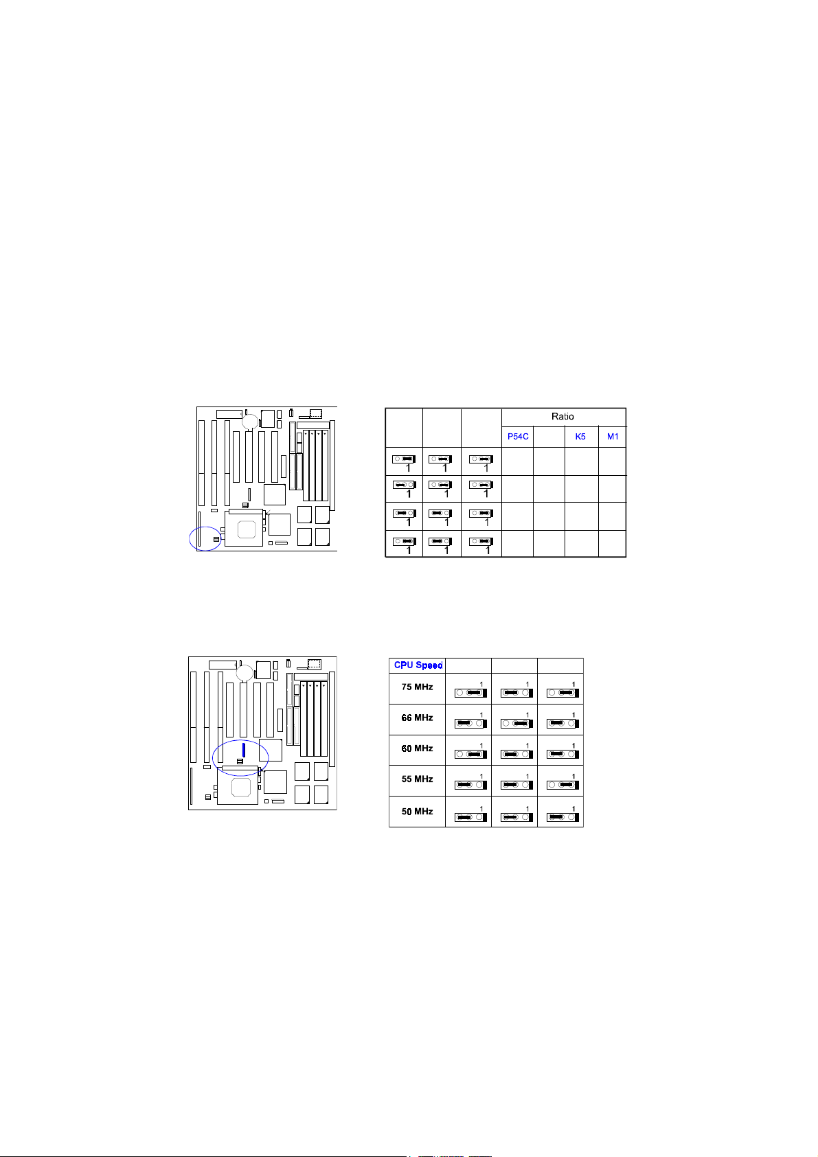
CPU to Bus Frequency Ratio: FREQ1, FREQ2, FREQ3
These three jumpers are used in combination to decide the ratio of the internal
frequency of the CPU to the external frequency (called the Bus clock) within the
CPU. These must be set together with the following jumpers (CPU external clock
Bus frequency).
CPU External Clock (Bus) Frequency: JCK1, JCK2, JCK3
The table below shows the jumper settings for the different CPU speed
configurations.
FREQ3
FREQ2
FREQ1
1.5 x 3.5x 1.5 x 3 x
2x
2x
2x 2x
2.5 x 2.5 x 1.75 x 1 x
3x 3x 4x
FREQ2 FREQ3
FREQ1 P55C
M2/K6
JCK3
JCK2
JCK1
Clock
Gen.
JCK1 JCK2 JCK3

Intel Pentium CPUs
Frequency
233 MHz
200 MHz
166 M Hz
Pentium MMX
Pentium
JCK1 JCK2 JCK3
JCK3
JCK2
JCK1
FREQ3
FREQ2
FREQ1

Voltage
These jumpers set the voltage supplied to the CPU. The voltage regulators will
automatically detect and switch between Single Power Plane and Dual Power Planes.
XXX
XXXXXXX
[P 5 5 C p h o to ]
A Pentium P55C
P
r
o
c
e
s
s
o
r
A Pentium P54C
Processor
XXX
XXXXXXX
[P54C photo]
JPW1 JV1
5
VRE
JV1
JPW1

AMD-K5/-K6 CPUs
Frequency
K6-200
K6-166
K5-PR200
K5-PR166
K5-PR150
K5-PR133
K5-PR120
K5-PR100
K5-PR90
200 MHz
166 MHz
133 MHz
116 MHz
105 MHz
100 MHz
90 MHz
100 MHz
90 MHz
66 MHz
66 MHz
66 MHz
60 MHz
60 MHz
3x
2.5 x
2x
1.75 x
1.75 x
1.5 x
1.5 x
1.5 x
1.5 x
66 MHz
JCK1 JCK2 JCK3
JCK3
JCK2
JCK1
FREQ3
FREQ2
FREQ1
Table of contents
Other FIC Motherboard manuals


Popular Motherboard manuals by other brands


Linear Technology
Linear Technology DC1362A-A Demo Manual

Linear Technology
Linear Technology DC2491A Demo Manual

Linear Technology
Linear Technology DC2117A Demo Manual

Shuttle
Shuttle Spacewalker AB30 user manual

Linear Technology
Linear Technology DC2166A Demo Manual

Analog Devices
Analog Devices Linear Technology DC2737A Demo Manual