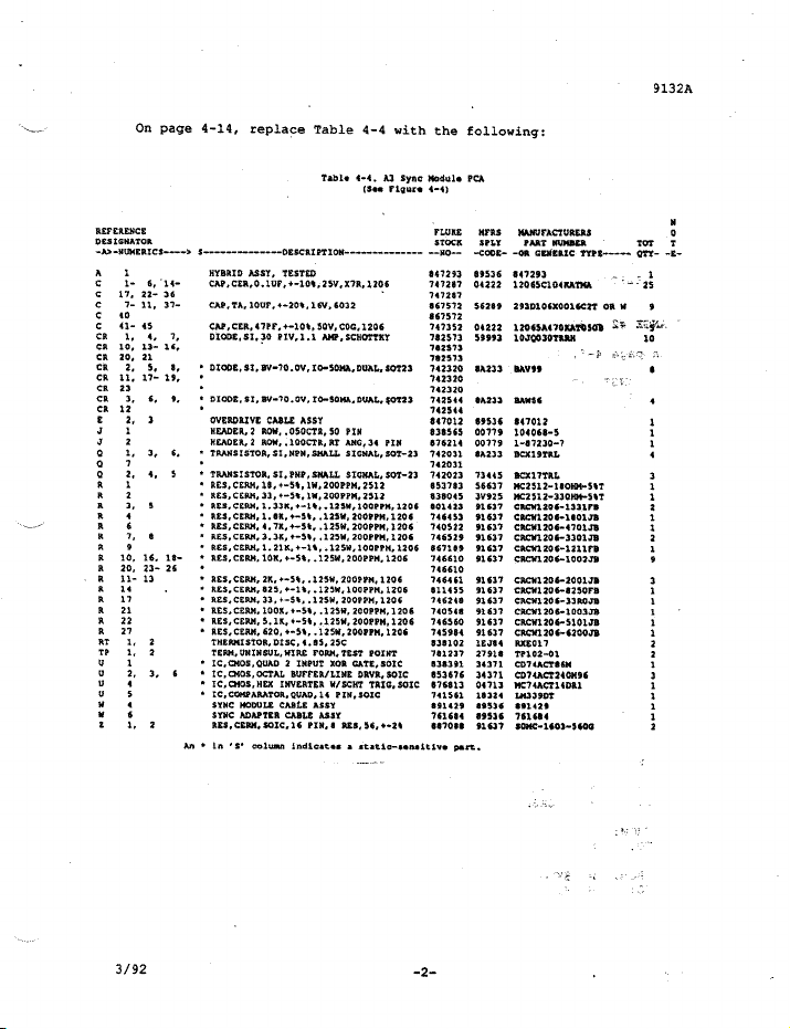
Fluke 9132A User manual

9132A
Service Manual
PIN 752857
November 1989 =Lu) Kf=
©1989 John Fluke Mfg. Co., inc., all rights reserved. Litho in U.S.A.

WARRANTY
COVERAGE
Fluke warrants the 9132A Memory Interface Pod to be free from defects in material and workmanship
under normal use and service for a period of ona (1) year from the date of shipment. The warranty does
not cover parts that connect directly to the Unit Under Test (flying lead sets, microprocessor sockets,
clips, headers, and Sync Adapter assemblies). This warranty extends only to the original purchaser and
does not apply to any product that has been misused, altered, or has been subjected to abnormal
conditions of operation.
Fluke's obligations under this warranty is limited to repair or replacement of aproduct that is returned to
an authorized Service Center within the warranty period, provided that we determine that the product is
defective. ¥we determine that the failure has been caused by misuse, alteration, or abnormal conditions
of operation, or if the warranty period has expired, we will repair the Pod and bill you for the reasonable
repair cost.
SERVICE
iafailure occurs, send the product, postage prepaid, to the closest Service Center with adescription of
the difficulty. Repairs will be made or the product replaced, and it will be returned, transportation prepaid.
Fluke assumes NO risk for damage in transit.
DISCLAIMER
THE FOREGOING WARRANTY IS EXCLUSIVE AND IN LIEU OF ALL OTHER WARRANTIES,
EXPRESS OR IMPLIED, INCLUDING BUT NOT LIMITED TO ANY IMPLIED WARRANTY OF
MERCHANTABILITY, FITNESS, OR ADEQUACY FOR ANY PARTICULAR PURPOSE OR USE.
FLUKE SHALL NOT BE LIABLE FOR ANY SPECIAL, INCIDENTAL, OR CONSEQUENTIAL
DAMAGES, WHETHER IN CONTRACT, TORT, OR OTHERWISE.
’
GETTING ANSWERS AND ADVICE
To enhance your use of this Pod, Fluke will be happy to answer you questions about applications and use.
Address all correspondence to: JOHN FLUKE MFG. CO. INC, P.O. BOX 8080, EVERETT,
WASHINGTON 98206-9090, ATTN: Sales Department,
JOHN FLUKE MFG. CO., P.O. BOX 9090, EVERETT, WASHINGTON 88206-9090

CHANGE/ERRATA INFORMATION
ISSUE NO: 13/92
This change/errata contains information necessary to ensure the accuracy of
the following manual. Enter the corrections in the manual if either one of
the following conditions exist:
1. The revision letter stamped on the indicated PCB is equal to or
higher than that given with each change.
2. No revision letter is indicated at the beginning of the
change/exrata.
MANUAL
Title: 9132A service
Print Date: November 1989
Rev.- Date: m=
C/E PAGE EFFECTIVITY
Page No. Print Date
3/92
3/92
3/92
3/92
=
WN

9132a
CHANGE #1 ~39582
Rev. -E, A3 Sync Module PCA (9132A-4002A)
On page 4-14, Table 4-4, make the following changes:
DELETE: J2|HEADER,Z ROW, .100CTR,RT ANG,20 PIN|500447/00779{1~87230-0}1}1
CHANGE: J2|[HEADER,2 ROW, .100CTR,RT ANG,14 PIN|757443100779187230~-7 {141
TO:. .J2|HEADER,2 ROW, .100CTR,RT ANG, 34 PIN|876214100779{1~87230-7{1
DELETE: NOTE 1 = P/N’s 500447 and 757443 are mounted next to each other
to form one .34-pin connector (J2).
©©ds
CHANGE #2 r,:39648
On page 4-5, Table 4-1,
CHANGE: MP5{TOP COVER ASSY/SELFTEST DOOR,PAINTED{792846189536]792846(1
TO: -MPS|TOP COVER ASSY/SELFTEST DOOR, PAINTED |886049{89536(886049(1
CHANGE #3 ~40220,41073
Ver. 2.0
On page 4-10, Table 4-2, make the following changes:
FROM: U32 |*PROGRAMMED PAL 1857495189536185749511
TO: U32 |*PROGRAMMED PAL, V2.0 1879916189536187991611 _—
FROM: U89 |*PROGRAMMED PROM, LO BYTE 1857487189536(85748711
TO: UB9, 90 |*PROGRAMMED PROM SET, V2.01889779189536188977911
DELETE: US0{*PROGRAMMED PROM,HI BYTE 1857482(895361857482{1
CHANGE #4 ~42111
On page 4-5, Table 4-1,
CHANGE: MP12|LABEL, VINYL, .3,1.5,BAR CODE|844712/89536184471211
TO: MP12 NAMEPLATE, SERIAL REAR PANEL|472795185480(472795]1
CHANGE #5 ~448795
The 9132FT-4002 A3 Sync Module is replacing the 9%132A-4002,
On page 4-5, Table 4-1, make the following changes:
FROM: MP14|CASE TOP, SYNC MODULE,PAD TRANSFER{8553791{895361855379{1
TO: MP14|CASE TOP, SYNC MODULE, PAD TRANSFER|894642{89536)89464211
FROM: MP16|DECAL, SYNC MODULE {844139189536184413911
TO: MP16{DECAL, SYNC MODULE|881424189536{891424|1
FROM: W4|SYNC MODULE CABLE ASSY{785584(89536{785584]1
TO: W4 |SYNC MODULE CABLE ASSY(|891429189536189142941
3/92 -1-

On page 4-14,
Table 4-4. Al Sync Module
(Sas Flgure 4-4)
FLUKE
STOCK
weRQum
847293
747287
147287
867572
867572
747352
782573
782873
782573
742320
742320
742320
742544
42548
847012
838565
876214
742031
742031
742023
853783
838045
201423
746453
740522
746529
#67109
746610
745610
746461
$11455
746248
740548
746560
745984
838102
181237
833391
853676
876813
T4156
£91429
761684
ss7088
MFRS
seLy
“CODE
89536
04222
$6289
04222
53993
A233
8A233
89536
00779
00779
A233
T3445
56637
3vezs
91637
91637
91637
91637
91637
91637
1637
91637
91627
91637
91632
91637
REFERENCE
DESIGHATOR
UM 127"
A1HYBRID ASSY, TESTED
<1-6, '14= CAP, CER, 0.1UF, +~108,25V,X7R, 1206
<17, 22-36 *
Cc 7-13, 37- CAP, TA, 10UF, +~20%, 16V, 6032
< 40
C41-45 CAP, CER, 47BF, +=10%, 50V, C0G, 1206
CRY, 4, 7, DIODE, S$I,30 £1IV,1.1 AMP, SCHOTTKY
CR 10, 13- 16, :
CR 20, 21
CR 2, 58, *DIODE, $I, BV=70.0V, 10=50MA, DUAL, $0723
CR 11, 17- 13, *
CR 23 =
CR 3, 69, *DICQDE, $I, BV=~70.0V, IO=$0MA, DUAL, §0T23
CR 12 *
t2, 3QVERDRIVE CABLE ASSY
J1HEADER, 2ROW, ,050CTR, 50 PIN
J2HEADER, 2ROW, .100CTR, RT ANG, 34 PIN
Qe i, 3, 6, *TRANSISTOR, SI, NPN, SMALL SIGNAL, S0T~23
Q7*
Q2, 45*TRANSISTOR, ST, PNP, SMALL SIGNAL, $OT-23
R1*RES, CERM, 18, +-5%, IW, 200PPH, 2512
R2*RES,CERM, 31, +~5%, IW, 200PPN, 2512
R3, 8©RES, CERM, 133K, +-1%, .125W, 1002PN, 1206
R4*RES, CERM, 1.8K, +~5%, (125W, 2000PH, 1206
Ré«RES,CERM, 4, 7K, +~5%, .125W, 200PPN, 1206
R7, *RES,CERM, 3.3K, +~5%, (125W, 200PPM, 1206
R9*RES, CERM, 1,21K, +-1%,.125W,100PPN, 1206
R16, 16, 18- * RES,CERM, 10X, +-5¢, 125W, 200PPN, 1206
R20, 23- 26 *
R11-13 *RES, CERM, 2K, 4-54, ,125W, 200PPN, 1206
R24 .*RES,CERM, 825, +-1%, .125W, 100PPH, 1206
R17 *RES, CERM, 33, +~5%, ,125W, 200PPM, 1206
R21 *RES, CERM, 100K, +~5%, ,125, 2008PM, 1206
R22 *RES, CERM, 5.1K, +-54, .125W, 200PPN, 1206
R27 *RES,CERM, 620, +~5%, .125W, 200PPM, 1206
RT i, 2THERMISTOR, DISC, 4.98, 25¢C
T® i, 2TERM, UNINSUL, WIRE FORM, TEST POINT
u1*1C,CMOS,QUAD 2INPUT XOR GATE, SOIC
u2, 3€+1C, CMOS, 0CTAL BUFFER/LINE DRVR, SOIC
u4*IC, CMOS, HEX INVERTER W/SCHT TRIG, SOIC
u5¢IC, COMPARATOR, QUAD, 14 PIN,S0IC
Ww 4SYNC MODULE CABLE ASSY
»6SYNC ADAPTER CABLE ASSY
z1, 2RES, CERM, SOIC,16 PIN, 8RRS, 36, 42%
An *in ‘S* column indicates astatic-sensitive part.
3/92 ww
replace Table 4-4 with the following:
9132A
N
MANUFACTURERS 0
PART NUMBER :TOT T
-OR GENERIC TYPEw-wen QTY~ ~E-
947293 1
12065C104RATMA a5
293D106X0016C2T OR W9
17065A070KATOSOD SF Fags
10
100030 TARE
Jeb
BAVSS
BAWSS
847012
104068-3
1-87230-7
BCXISTRL
BCX1TTRL
MC2512-180HM-SAT
MC2512-330KM-54T
CRON1206~1331F8
CRCW1206+180108
CRCW1206~4701J8
CRCWL206-330108
CRCW1206-1211FD
CRECW1206-100209
CRCW1206~200178
CRCW1206-8250FB
CRCWY206-33R058
CRCW1206+-100308
CRCW1206~510108
CRCW1206-$20008
CDTAACT240M9€
761684
S0MC~1603~560G
-
a
fT
EE
LL
an

91i32a
On pages 4-15 and 5-21/5-22, Figure 4-4 and Figure 5-3, replace the
schematic and reference designator drawings with the following:
B
RE cm i
eeancUke
9132FT-1602
~3-

9132a
10
kan
80AR0
mun
HHT
.P—
SHIELD
TOWECTION
SHOW
TEST
POINTE
}
ail
28258 201 rr
ue
alfa
2
12
E52
,
en
aetrts
[een
Sd
ow aPe
3
EY oh
wom
ow
oa
on fr]
wceeolis
__€8
|sPM
wr
FR
ow
no
[ns
Ex
vw om
n
0
wy
te
pava3
[8
wre “® om oa aaoe on
acess
wt
Agser
5.8
av Yec
o- et eon ovespazve
to
3/92 -4- 8132FT-1002

IMPORTANT NOTE
Use of the 9132A Interface Pod requires that the 9100-Series
Mainframe have software installed that is version 4.0 or later.

9132A Service
Table of Contents
SECTION TITLE PAGE
1INTRODUCTION AND SPECIFICATIONS ..covuecemeeecrneemrorenssnsmenens 1-1
1-1. INTRODUCTION 1-1
1-2. SPECIFICATIONS 1-1
2THEORY OF OPERATION 2-1
2-1. GENERAL THEORY OF OPERATION.
2-2. THEORY OF OPERATION.......c..ccoevrmemenn.
2-3. Main Board Kernel
2-4. Main Board Sync Generation Timing.....c...ceeovrvererenresniennnn.
2-5. Main Board Emulation RAM Connectors and Self Test.
2-6. Main Board Emulation RAM Control ...
2-7. Main Board Input/Output Devices.........
2-8. Main Board Address RAM and Sync Module Interface.
2-9. Main Board ROM Module COnnections........c.emmseemsessssresrsnsens 212
2-10. Sync Module 2-12
2-11. ROM Modules (24-, 28-, and 32-Pin Assemblies) .....c.ooeureirennes 2-13
2-12. ROM Plug Adapters 2-14
2-13. Self Test Assembly 2-15
2-14. RAM Module or Emulation RAM..... vase 2-15
2-15. Personality Module 2-15
2-16. Sync Adapters 2-16
3 MAINTENANCE 3-1
3-1. INTRODUCTION 3-1
3-2. WARRANTY AND FACTORY SERVICE... 32
3-3. INSPECTING ASHIPMENT .......ccccrumirvinnnne ee 3-2
3-4. SHIPPING THE POD TO FLUKE
FOR REPAIR OR ADJUSTMENT... 3-2
3-5. MAINTENANCE PROCEDURES. ...... wis 3-2
3-6. Cleaning 3-2
3-7. Changing the Fuses on the Sync Module...... 3-3
3-8. Changing the Fuse on the ROM Module .3-3
3-9. INSTALLING THE PLUG-IN MODULES .3-3
3-10. Installing the Personality Module ...... .3-4
3-11. Installing the Sync Module ........ 3-5
3-12. Installing the ROM Module(s) .3-5
3-13. Installing the RAM Module(s)........... ee 3-6
3-14. Closing the Pod Case 3-7
3-15. CONNECTING THE POD TO THE MAINFRAME 3-7
3-16. USING THE POD SELF TEST............ 3-7

9132A Service
TABLE OF CONTENTS, continued
SECTION TITLE PAGE
7. TROUBLESHOOTING PROCEDURES.......
8. Preparation for Troubleshooting the Pod.
9. Running the 9132A Service Test .....cvuvweeen.
-20. DISASSEMBLY
1. Removing the Main PCA..........
2. Removing the Self Test PCA...
3-23. Removing the ROM Module PCA.
3-24. Removing the Sync Module PCA............
4LIST OF REPLACEABLE PARTS ..ccovvvevernmssmrarasmcnssenssnncsnnmnssosasase 4-1
4-1. INTRODUCTION
4-2. HOW TO OBTAIN PARTS......ccoeorvnrrnnee
4-3. MANUAL STATUS INFORMATION
4-4. ADDITIONAL INFORMATION
4-5. NEWER INSTRUMENTS ......
5 SCHEMATIC DIAGRAMS 5-1

9132A Service
List of Tables
TABLE TITLE PAGE
2-1. State Definitions for the Sync State Machine........cooevecevsinnrenssnesesens 2-12
3-1. Pod Self Test Failure Codes. 3-10
3-2. Required Test Equipment for Pod Troubleshooting .........ccvcecrvvnresrsrnens 3-12
4-1. 9132A Final Assembly 4-5
4-2, Al Main PCA 4-10
4-3. A2 Self Test PCA 4-13
4.4, A3 Sync Module PCA 4-14
4-5, A4 RAM Module PCA 4-16
4-6. ROM Module Final Assembly.......... 4-18
4-7. AS ROM Module PCA 4-20
4-8. A6 ROM Plug Adapters 4-22
4-9. Manual Status Information 4-24
iiifiv

FEY
FIGURE
Bp
bE
PRPRREEREDE
DEUS
hABRRUAGARON
§
Gh
Lh
A
BB
5-6.
bw
9132A Service
List of Figures
TITLE PAGE
9132A Memory Interface Pod Block Diagram..........cevueionnnererseerrirones 2-2
Sync Generation 2-4
Opening the Back Panel of the Pod 3-4
Installing the Personality Module... -4
Connection of the External Module .3-5
Connecting the RAM Modules........ccorerermruenrsirocnee .3-6
Connection of the Interface Pod to the Mainframe. 3-7
Connecting the ROM and Sync Modules to the Self Test PCA .............. 3-9
Connecting the Test Equipment 3-13
Service Test Program Menu 3-14
9132A Final Assembly 4-6
Al Main PCA 4-12
A2 Self Test PCA 4-13
A3 Sync Module PCA 4-15
A4 RAM Module PCA 4-17
ROM Module Final ASSembly .....cccowmiccreveinncresiicinisimisnisessssessnons 4-19
AS ROM Module PCA
scons
simiam
anim 4-21
A6 ROM Plug Adapters 4-23
Al Main PCA 5-3
A2 Self Test PCA 5-19
A3 Sync Module PCA 5-21
A4 RAM Module PCA 5-23
A5 ROM Module PCA 5-25
AG ROM Plug Adapter 5-27
vivi

9132A Service
==. Section 1
Introduction and Specifications
INTRODUCTION 1-1.
This manual presents service information for the 9132A Memory Interface
Pod. Included are a theory of operation, general maintenance procedures,
performance tests, troubleshooting information, alist of replacement parts,
and schematic diagrams. This manual does not include information on the
Processor Support Packages. The Processor Support Packages contain no
serviceable parts.
SPECIFICATIONS 1-2.
The specifications for the 9132A can be found in the individual
microprocessor-specific user’s manual (i.e., the 9132A-80386 User's
Manual for the 80386 processor, the 9132A-68020 User's Manual for the
68020 processor, etc).
111-2

9132A Service
Section 2
Theory of Operation
GENERAL THEORY OF OPERATION 2-1.
The 9132A (referred to hereafter as the Pod) interfaces the 9100-Series
Mainframe to aunit under test (UUT). The Pod receives commands from
the Mainframe and processes the commands so they can be executed on the
UUT. The 9132 is amemory emulation Pod, that is, it takes control of the
UUT’s memory and uses the processor on the UUT to execute the Pod’s
commands. To do this, the Pod plugs into or attaches to the UUT Boot ROM
sockets, effectively replacing the memory in them. The other feature required
for controlling the UUT is the ability to drive or overdrive the UUT reset line.
To take command or control of the UUT, the Pod resets the UUT and the
code that originally came from UUT boot ROMs is replaced by the code from
the Pod. This code then executes the user's instructions.
The Pod also monitors some microprocessor lines directly. Eight lines for
timing control (either status or control lines) monitor the state of the UUT
microprocessor. Basically, these lines form a“sync” signal used by the
Mainframe or user at arequired access time. The other use of the sync
signal is for returning data. Eight data lines are also monitored and
functionally return data from the UUT’s microprocessor to the Pod by means
of byte writes to an address called a“transfer address”. When this
operation occurs, the sync pulse (generated from the Pod) loads the data at
the microprocessor data bus into alatch, which can be read by the Pod.
THEORY OF OPERATION 2-2.
Ablock diagram of each major Pod section is presented in Figure 2-1. Each
major section is described in the following paragraphs. Component
designators such as “Uxx” and signal names refer to schematic diagrams in
Section 5.
NOTE
Signal names appear as in the schematic diagrams.
Signal names that end in “-” (e.g., BERR-) indicate an
active state at low voltage.
Main Board Kernel 2-3.
The Main Board kernel circuitry is shown on page 1of the Main Board
schematic (Figure 5-1).

9132A Service
Pe
a
a
mm
i
tn
mm
fr
tm
fi
fo
i
i
me
inn
|
MOOD
FAD
snd
I
Wod
ve
ot
S1HOd
TENGEN
||
TENE
aod
Of
god
|
3804d
300930
Jom,
|
C3ZINOUHONAS
!
ssauaay
NEE
|
|
|
1
|
!
2:
]
|
|
wou
|
4
EEE
EEE
|
SSH
I
re
|
|
rd
=)
I
i
[Ed]
sag
1
El
n3Lsas
-
Femme
Po
1353
|
INHAHANO
id
mas
me
sim
st
ren
re
mn
id
gr
me
me
L1Z4N
ZN
€
TANNVHO
|
1
SAIICHINO
1
__
FINO
ONAS]
|
ATTN
v
|
OHINOD
FNLAHIAC
bel
a
|
;
!
L
EI]
I
|
i
LL
L
|
i
[
wv
we
HOV
Nn
HOLVYENID
|
{
1
YHZANY
NOLLYINWI
Yivg
ONAS
1
!
A
:
|
ir]
snd]
i
|
|
i
!
!
|
I
CHYOS
3OVIHIINI
AHOWSW
am
mr
sr
i
i
om
oe
i
Sn
nt
SS
oe
St
Sm
So.
mn
Tt
So
Lr
rt
re
en
ee
i
Si
tt
St
ni
rr
rome
nm
i
st
re
en
2d
Figure 2-1. 9132A Memory Interface Pod Block Diagram
2-2

9132A Service
The heart of the Pod is a68000 microprocessor (U92). The processor is
reset by the RESET- line. This line is produced either by the PODRESET-
line from the Mainframe or by the power-up reset RC network. The BERR-,
BR-, and BG- signals are not used during operation. The interrupt lines
(IPLx) are all tied high through 4.7K-ohm resistors. An 8-MHz oscillator
(U91) clocks the processor.
The main address decoding is achieved by an HCT138 (U40). U40 divides
the address space into several 64K segments. Each of the lines that select
the segments begins with a specific letter that identifies its destination. If
the line begins with “K”, such as KROMSEL-, the Krefers to kernel, as in
kernel ROM select or kernel RAM select. “P” refers to personality, such
as PMROMSEL- or Personality Module ROM select. “A” refers to ad-
dress, such as ARAM-SEL or address RAM select. “E” refers to emula-
tion, such as ERAMSEL- or emulation RAM select. U40 also has lines for
output port select (QUTPORTSEL-) and input port select INPORTSEL-).
The port selects from U40 are divided by three ACT138s (U83 and U73 are
output port decoders, and U3 is an input port decoder) into the output port or
input port selects. Each output port select is divided into high and low
bytes, and can be written to either as abyte or a word (i.e., U83 and U73
can be selected at the same time or either one can be selected individually).
The outputs from U83 correspond to the high data lines, and the outputs
from U73 correspond to the low data lines. Extra decoding for U83 and U73
is provided from the UDS- and LDS- lines from the microprocessor, which
are gated to write lower (WL-) and write upper (WU-). WL- and WU- are
active during awrite cycle if LDS- and UDS- are active. Aword write
forces both data strobes active, which in tum activates WL- and WU- at
the same time.
ERAMSEL- on pin 11 of U40 is further broken down into ERAMASEL- and
ERAMBSEL- through U28. These signals are the bank selects for the
emulation RAM (ERAM). The state of AlS5 determines which bank of
RAM is selected (A15 low =bank A, A15 high =bank B).
The kernel ROM consists of two 32K x8CMOS ROMs (U90 and U89).
The kernel RAM consists of two 32K x8 static RAMs (U95 and U88).
Self test enable is determined by A23 and interrupt acknowledge. If any
access that is not an interrupt acknowledge occurs while A23 is high, it is
counted as a self test access. These accesses pulse self test latch enable
(ST-LE), the output of U16 pin 13. If the access is aread, aself test output
enable (ST-OE-) occurs. These signals disable all internal accesses and
access only the self test ports when A23 is high.
Main Board Sync Generation Timing 2-4.
The Main Board sync generation timing circuitry is shown on page 2of the
Main Board schematic (Figure 5-1). AMain Board sync generation timing
block diagram is shown in Figure 2-2.
A16-bit address comparator looks at the address lines of ROM Module 1.
(The various signals coming onto the main Pod board are, for example,
labeled ROM1IPIN28 or ROMIPIN3.) These are the address lines of the
boot ROM coming from the ROM Module. Other types of inputs entering
2-3

9132A Service
MEMORY EMULATION POD
REFERENCE Em)
ADDRESS F<
COUBRRE.
EQUAL VALID-COMPARE
COMPARATOR femme] ©aCOUNT-ENABLE
BER
rooness meri
Ibel pa [sYNCPULSE
©
AEAs :
[SINC
uLsE,
CYCLE CLOCK
|SOUT >
ol
COUNTER
VALID ADDRESS OR A
DATASYNC-CLK
Figure 2-2. Sync Generation
the comparator are, for example, ROMIPIN28POL, which chooses if the
existing pin is high or low for the compare, and ROMIPIN28DC-. When
ROMIPIN28DC- is low, the comparator does not care about the state of
ROMIPIN28. This type of architecture is used throughout the comparator.
The output of the comparator is summed by U29, an 8-input NAND gate.
Two other pins are input to U29. ROMISEL-, an output from ROM Module
1, reports that the output enable and chip enable on the module are active.
ROMIDC- is adon’t care signal for the ROM1SEL- line. When all the pins
into U29 are active, the output of the comparator, COMPAREQ- (U29 pin
8), goes active low.
The output of the comparator is sampled by BCYCLECLK- (BCYCLECLK-
is explained in more detail further on in this section). BCYCLECLK- is a
clock to U21B, an AC74 Flip-Flop. Once the latch is set, it stays set using
the OR gate (U37C) until forced to clear by a reset or rearm signal at U21
pin 13. The comparator signal COMPAREQ- recognizes events occurring at
the ROM Modules. When COMPAREQ- is received at U21 and
BCYCLECLK- is active, the clock latch output goes true.

9132A Service
In some modes the CLKLATCH output from U21B clocks the Ul3 latch
(U13 is shown on page 5of the Main Board schematics). This latch receives
the low eight addresses from ROM Module 1. When CLKLATCH goes
true, U13 is latched and the lower 4 bits of UUT ROM address latched into
U13 allow the Pod to receive status information from the UUT.
Asmall circuit composed of U9 and U28D creates the overdrive reset
(OVDRV-RESET) signal. The inputs to this circuit are reset request
(REQRESET), aline that is written to or controlled by the processor,
ABORT, aline that comes from the Mainframe, and enable abort (EN-
ABORT), aline from an output port on U86 (UB6 is shown of page 5of the
Main Board schematics). This circuit allows three methods of overdriving
the UUT. If the REQRESET line from the Pod goes high, the overdrive reset
(OVDRV-RESET) line forces the Pod to overdrive the reset of the UUT. If
the EN-ABORT line to the circuit is active, either the ABORT line from the
Mainframe or the clock latch from U21B (preset as acomparator for a
breakpoint) can be used to overdrive the UUT.
CLKLATCH is cleared either by aRESET- (from the Mainframe or power-
up reset) or by the output port signal REARM.
The bank switch lines from U4 and U24 allow the Pod to switch between
two banks of emulation RAM. The ERAM bank switch circuitry allows the
Pod to switch cleanly between banks of RAM without causing metastable or
timing problems.
Two signals called force bank A(FRCBANKA) and force bank B
(FRCBANKB) enter the bank switch circuit at Ul6. (FRCBANKA and
FRCBANKB are output port bits controlled by the Pod processor.) If both
FRCBANKA and FRCBANKB are true, both banks of ERAM are available
to the Pod and, consequently, not available to the ROM Modules. If only
one of the banks is forced, the forced bank is available to the Pod processor,
but the other bank is available to the ROM Modules.
Using force bank to switch banks is nonsynchronous and can cause runtime
problems with the UUT processor. To make aclean swap between banks,
the PLZACCBNKA/-B line is used to switch banks when BCYCLECLK- is
cycled.
The AND/OR gate (U19) that the swap select (SWAP-SELECT) line
enters allows two different ways to initiate aswap. When SWAP-SELECT
is set in one mode, the next true BCYCLECLK- that clocks U27B swaps
the banks. When SWAP-SELECT is in the other mode, SC11 (the sync
counter output) is used for swap select when the Pod goes into RUNUUT
mode. This type of swap has two accesses. U27B gets swapped on the
first clock and is then set and ready. (At that time, when U27B is swapped
and U27A is not, neither bank is available to the Pod processor. Whichever
bank was available to the ROM Module is still available.) On the next
clock cycle, when BCYCLECLK- clocks pin 3of U27A, the actual swap
occurs. ‘This swap occurs regardless of which mode was selected; it is the
BCYCLECLK- after the first bank is swapped that actually causes the bank
swap. This prevents metastable conditions caused by the delay between
the two flip-flops (U27) that could produce an indeterminate output state.
2-5

9132A Service
The outputs of the U27 flip-flops are ANDed for ROM bank select
(ROMBANKSEL) and bank available (BANKAAVAIL, BANKAAVAIL-,
BANKBAVAIL, and BANKBAVAIL-). These five lines select which bank
is available to the Pod processor, which bank is available to the ROM
Module, and which bank has readable bits.
RUNUUT 1, 2, 3, and 4are separate outputs to ROM Modules 1, 2, 3, and 4.
These lines control chip enable (CE) and output enable (OE) for the UUT
boot ROMs located in the ZIF socket of the ROM Modules. U21A is the
RUNUUT flip-flop. This flip-flop is set by RUNUUTREQ to the data input
pin (pin 2) and the sync counter output (SC11) to the clock input pin (pin 3).
The flip-flop is swapped when the Pod is in RUNUUT mode and the SC11
line goes true. (In some hardware modes, SC11 can be forced by the
processor to not be atrue timer signal) The AND/OR gates U4C and U37D
allow aread from the boot ROM plugged into the UUT ROM Module to
occur, dynamically switching the ROM Module in and out of RUNUUT mode
for one bus cycle. This switching occurs only if sync mode is set to data
sync (because this is the only time that data is valid). Once the SYNC line
goes active, one bus cycle is clocked to Pod sync if the Pod is in data sync
mode with the ROM-TST-EN bit set. When the clocked bus cycle occurs,
the ROM Modules switch the emulation RAMs out and the ROM in, which
lets the UUT processor read the data that is located in the UUT ROM.
Main Board Emulation RAM Connectors and Self Test 2-5.
2-6
The Main Board Emulation RAM connectors and self test circuitry are
shown on page 3of the Main Board schematic (Figure 5-1).
J12, 113, J14, and J15 are the sockets for the emulation RAM Modules. For
each ROM Module connected to the Pod, acorresponding RAM Module is
plugged into these sockets. Each RAM Module has two banks. The lines
into these connectors are bank enable, and address and data lines in and
out. The emulation RAM Modules are explained further on in this section.
The self test board connector is attached by aribbon cable to the self test
board. Self test is accessed when A23 is high. During self test read or
write, all other address lines go to the address latches U104, U23, and U76.
When self test latch enable (ST-LE) is true, these latches are transparent,
allowing the addresses to go straight to the different self test pins. At the
end of self test, the addresses that are latched remain stable and do not
change until the next self test access.
The data path from the self test board connector goes to U100 and U103,
which are noninverting data buffers. Whatever is on the pins is gated to the
Pod data bus when self test output enable (ST-OE) is true (i.e., during any
self test read).
One of the pins on the ROM Module (pin 24, 28, or 32) must have +5V
power when plugged into the self test socket. Three relays (K1, K2, and
K3) switch power to the appropriate pin, depending on the type of ROM
Module. The self test control lines (SLFTST-CNTL-28, SLFTST-CNTL-
30, and SLFTST-CNTL-32) choose which of the relays is activated.

9132A Service
Main Board Emulation RAM Control 2-6.
The Main Board Emulation RAM control circuitry is shown on page 4of the
Main Board schematic (Figure 5-1).
The Pod processor can switch control of read and write to either bank of
emulation RAM on the RAM Module(s). In normal mode, the Pod
processor can read and write to one bank of emulation RAM while the other
bank is being used by the ROM Modules. The bank available lines
(BANKAAVAIL and BANKBAVAIL) select the mode of the different
muxes (U65, U72, U69, U81, U74, U71, U78, and U80). Depending on the
state of BANKAAVAIL and BANKBAVAIL, either the address lines from
the Pod processor or the ROM Module 1address bus (ROMADDR) are
used by the emulation RAM.
Two of the bank available muxes ICs (U65 and U74) perform a four-to-one
mux (as opposed to two-to-one by the others). Emulation RAM address
12 and emulation RAM address 11 require the four-to-one mux because
some ROMs, such as the 2364, switch pin numbers of address lines All
and A12. The positions of RAM address 12 and 11 allow software control of
the placement of A11 and A12 on the ROM.
Two other lines, called AI2ENABLE- and A11ENABLE-, are also sent to
U65 and U74. Since some ROM types use only 10 address lines,
A12ENABLE- and A11ENABLE- disable address lines All and A12 from
the RAM Module and hold them in astable condition while ROM Module 1
is not driving them.
Two latches (U68 and U93) delay the ROM address lines, allowing more
hold time for address traces. The lines are latched by an active
BCYCLECLK-. The address is latched at the end of the cycle and held. The
latches allow delayed clocking of the address RAM with no penalty since
the Pod holds the addresses on the outputs (i.e, DELAY ROMADDR)
until the next ROM access. Any time the BCYCLECLK- is active low, the
latches are transparent and the addresses pass straight through the
latches. Once the BCYCLECLK- goes high, U68 and U93 latch and hold the
last address until the next access.
Main Board Input/Output Devices 2-7.
The Main Board input/output device circuitry is shown on page 5of the Main
Board schematic (Figure 5-1).
Two data buffers (U102 and U101) pass the data from the Pod data bus to
the output data bus. The buffer outputs drive the inputs to all of the Pod’s
latched output ports.
All output ports on the output data bus are latched when the proper clock is
received. The clocking signal is an output port select (i.e., OUT2-, OUT4-,
etc.). Each of the ports can be written to as a pair or singly, depending on
the selected mode (selected as either aword or byte write). Most of the
ports are cleared on areset or power-up reset and all the outputs go low.
The ROMIPINXPOL outputs from U85, U54, and pin 12 of U86 control the
polarity of the ROM Module 1address bus signals that are allowed to pass
27
Table of contents
Other Fluke Test Equipment manuals

Fluke
Fluke 4180 Quick start guide

Fluke
Fluke 6270A User manual

Fluke
Fluke TP1000 Original instructions

Fluke
Fluke 9132 User manual

Fluke
Fluke 190-502/AM User manual

Fluke
Fluke 705 User manual

Fluke
Fluke TS22 User manual

Fluke
Fluke ProcessMeter 787 User manual

Fluke
Fluke Series II User manual

Fluke
Fluke 71 Series Use and care manual

Fluke
Fluke 150 Series Use and care manual

Fluke
Fluke 6055 User manual

Fluke
Fluke ScopeMeter 199C Instruction Manual

Fluke
Fluke 5700A Series II Service User manual

Fluke
Fluke 9103 User manual

Fluke
Fluke 190-102/AM/S User manual

Fluke
Fluke TL2X4W-TWZ User manual

Fluke
Fluke AIRCHECK User manual

Fluke
Fluke 154 HART User manual

Fluke
Fluke 5700A Series User manual