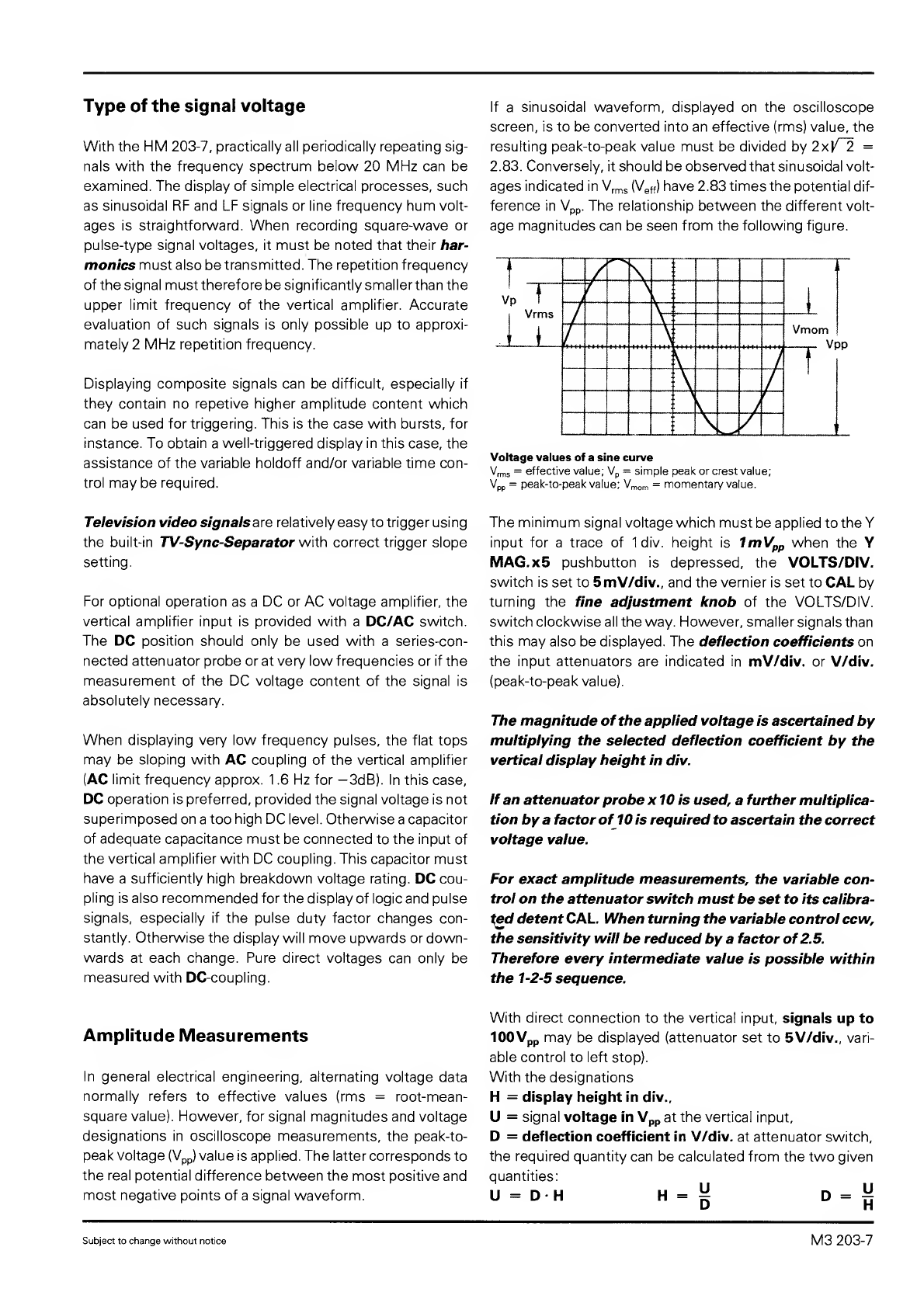
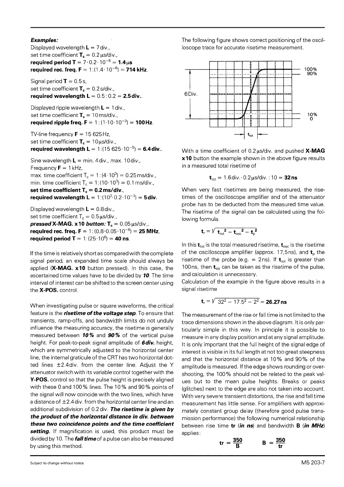
Hameg HM 203-7 User manual

Instruments
MANUAL
Oscilloscope
HM
203-7

Table
of
contents
Oscilloscope
datasheet
with
technical
details
.
P
1
Accessories
.Z
1
Operating
Instructions
General
Information
.Ml
Use
of
tilt
handle.
Ml
Safety.Ml
Operating
conditions.M2
Guarantee
.M2
Maintenance.M2
Switching
over
the
mains/line
voltage.M2
Type
of
the
signal
voltage
.M3
Amplitude
Measurement.M3
Time
Measurements.M
4
Connection
of
Test
Signal
.M
6
First
Time
Operation.M
7
Trace
Rotation.
M
7
Probe
compensation
and
use.
M
7
1
kHz
compensation.M
8
1
MHz
compensation.M
8
Operating
modes
of
the
vertical
amplifiers
....
M
8
X-Y
Operation.
M
9
Phase
difference
measurement
in
DUAL
mode
.
M
9
Measurement
of
an
amplitude
modulation
....
M10
Triggering
and
time
base.M10
Automatic
Triggering.M10
Normal
Triggering,
Slope.Mil
Trigger
coupling.
Mil
Alternate
Triggering.Ml
2
Line
Triggering.Ml
2
Triggering
of
video
signals.Ml
2
External
triggering,
Trigger
indicator.Ml3
Holdoff-time
adjustment.Ml
3
Component
Tester.Ml
3
Test
patterns.Ml
6
Short
instruction
K
1
Front
panel
elements
Folder
with
front
view
.K
2
Test
Instructions
General.T
1
Cathode-Ray
Tube;
Brightness
and
Focus,
Linearity,
Raster
Distortions.T
1
Astigmatism
Check.T
1
Symmetry
and
Drift
of
the
Vertical
Amplifier
.
.
.
.
T
1
Calibration
of
the
Vertical
Amplifier.T
1
Transmission
Performance
(Vertical
Amplifier)
.
.
.
T
2
Operating
Modes:
CH
I/ll,
DUAL,
ADD,
CHOP.,
INVERT
and
X-Y
Operation.T
2
Triggering
Checks
.T
3
Timebase.T
3
Holdofftime
.T
4
Component
Tester.T
4
Trace
Alignment.T
4
Mains/Line
Voltage
Checks.T
4
Oscilloscope
HM
203-7
Service
Instructions
General.SI
Instrument
Case
Removal.SI
Operating
Voltages.SI
Maximum
and
Minimum
Brightness.SI
Astigmatism
control.S
2
Trigger
Threshold.S
2
Trouble-Shooting
the
Instrument.S
2
Replacement
of
Components
and
Parts.S3
Replacementof
the
Power
Transformer.S3
Adjustments.S3
Circuit
Diagrams
Wiring
Diagram.D
1
Identification
of
electrical
components.D
2
Y-Inputs,
Attenuators,
Preamplifier
Channel
I
and
Channel
II.D
3
Y
Intermediate
Amplifier
Channel
I
and
Channel
II
Channel
Selection,
Component
Tester.D
4
Trigger
Circuit,
TV
Sync
Separator,
Calibrator.
.
.
.D
5
X
and
Y
Final
Amplifier.D6
Timebase
Circuit,
Trigger
Control.D
7
CRT
Circuit,
Unblanking
.D
8
Power
Supply.D
9
Component
Locations
EY
Board.DIO
Component
Locations
CO
(IF)
Board.DIO
Component
LocationsXY
Board.Dll
Component
Locations
TB
Board.D12
Subject
to
change
without
notice
5.91
•
203-7

OSCILLOSCOPE
HM
203-7
Specification
(
21
°
C;
ismin.)
Vertical
Deflection
Operating
modes;
Channel
I
orCh.
II
separate,
Channel
I
and
II:
alternate
or
chopped;
(Chopper
frequency
approx.
0.4
MHz).
Sum
or
difference
of
Ch.
I
and
Ch.
II.
(channel
II
invertible).
X-Y
Mode:
via
Channel
I
and
Channel
II.
Frequency
range:
2x
DC
to
20MH2
(-3dB).
Risetime:
approx.
17.5ns.
Overshoot:
^1
%.
Deflection
coefficients:
10
calibrated
steps
from
5mV/div.
to
5V/div
in
1-2-5
sequence.
Accuracy
in
calibrated
position:
±3%.
Variable
2.5:1
to
max,
12.5V/div.
Y-magnification
x5
(calibrated)
to
1
mV/div.
±5%
(frequency
range
DC
to
3.5MHz,
—3dB)
Input
impedance:
1
MQ
II
25pF.
Input
coupling:
DC-AC-GD
(Ground)
Input
voltage:
max.
400V
(DC
+
peak
AC).
Y-output
from
Ch.
I
or
Ch.
II
(optional)
Trigger
System
With
automatic;
10Hz-40MHz.
>0.5div.
normal
with
level
control
from
DC-40MHz.
Slope:
positive
or
negative.
ALT.
triggering
;
LED
indication
for
trigger
action.
Sources:
Ch.
I,
Ch.
II,
line,
external.
Coupling:
AC
(S10Hz
-10
MHz),
DC
(0
-10
MHz),
LF
(0
-
<50kHz),
HF
(>1,5kHz
•
40MHz).
Threshold
external
>0.3V.
Active
TV-Sync-Separator
for
line
and
frame.
Horizontal
Deflection
Time
coefficients:
18
calibrated
steps
from
0.2|is/div.
to
0.1
s/div.
in
1-2-5
sequence,
accuracy
in
calibrated
position:
±3%.
variable
2.5:1
to
max.
0.25s/div.,
with
X-Magnifier
x10
(±
5%)
to
==
20ns/div..
Hold-Off
time:
variable
to
approx.
10:1.
Bandwidth
X-Amplifier:
DC-3
MHz
(-3dB).
Input
X-Amplifier
via
Channel
II,
sensitivity
see
Ch.
II
specification.
X-Y
phase
shift:
<3°
below
220kHz.
Z
input
(optional)
Component
Tester
Test
voltage:
approx.
8.5Vm,5
(open
circuit).
Test
current:
approx.
8mA,(shorted).
Test
frequency:
^
line
frequency.
Test
connection:
2
banana
jacks
4mm
0.
One
test
lead
is
grounded
(Safety
Earth).
General
Information
Cathode-ray
tube:
D14-364
P43/123,
or
ER151
-GH/-,
rectangular
screen,
intern,
graticule.
8x10cm
Acceleration
voltage:
2000V,
Trace
rotation:
adjustable
on
front
panel.
Calibrator:
square-wave
generator
==
1
kHz
for
probe
compensation.
Output:
0.2Vand2V
+1
%.
Line
voltage:
110,
125,
220,
240
V~
±10%.
Line
frequency:
50Hz
to
400Hz.
Power
consumption
:
=
37
Watt
(at
50
Hz).
Max.
ambient
temperature:
-(-10°C...-T40°C.
Protective
system:
Safety
Class
I
(lEC
348).
Weight:
approx.
7.5kg.
Colour:
techno-brown.
Cabinet:
W
285,
H
145,
D
380mm.
Lockable
tilt
handle.
20
MHz
Standard
Oscilloscope
2
Channels,
max.
1
mV/div.
sensitivity;
Component
Tester
Timebase:
0,1s/div.
to
20ns/div.;
Variable
Holdoff;
Alternate
Triggering;
Triggering:
DC-40MHz;
TV
Sync
Separator;
Trigger
LED
The
HM
203-7
is
Western
Europe's
best
selling
oscilloscope
because
it
responds
thoroughly
to
customer
demands
for
reliability,
superior
perfor¬
mance,
and
ease
of
operation.
The
outstanding
transient
response
of
the
HM
203-7,
particularly
when
displaying
square
wave
signals,
is
one
of
the
pre-eminent
features
of
this
quality
instrument,
the
integrity
of
the
signals
reproduced
by
this
oscilloscope
reflect
a
dedication
to
engineering
excellence
normally
only
found
in
expensive
labora¬
tory
instruments.
As
an
aid
to
ensure
the
correct
polarities
when
displaying
the
sum,
difference,
or
video
signals,
an
"invert"
control
is
provided
on
channel
II.
Technically
advanced
triggering
circuits
enable
the
user
to
attain
clear,
stable
displays
from
DC
to
over
40
MHz,
with
input
levels
as
low
as
0.5
divisions.
The
Holdoff
control
enables
even
complex
asynchronous
waveforms
to
be
solidly
displayed.
Trigger
action
is
indicated
by
an
LED,
which
illuminates
whenever
the
trigger
threshold
point
is
crossed.
And
for
the
display
of
video
signals,
the
HM
203-7
has
a
low
distortion
active
TV
sync
separator,
which
allows
for
auto¬
matic
synchronizing
with
line
and
frame
frequencies.
"Alternate
triggering"
mode
enables
the
display
of
two
asynchronous
signals
simulteneously.
The
CRT's
8x10
cm
internal
graticule
enhances
parallax-free
viewing
over
a
wide
field.
In
addition,
the
CRT
is
fully
shielded
with
mumetal
to
prevent
display
distortion
in
the
presence
of
magnetic
fields.
As
a
practical,
built-in
feature,
the
component
tester
enables
the
operator
to
quickly
identify
faulty
semiconductors
and
a
large
variety
of
individual
compo¬
nents,
both
in
circuit
and
out.
The
HM203-7
was
specifically
designed
for
use
in
production
lines,
general
service
applications,
and
for
technical
training
facilities.
The
multiplicity
of
display
modes,
the
easy-to-understand
front
panel,
and
the
operational
simplicity
of
the
HM203-7
make
it
also
an
ideal
training
scope
for
educational
purposes.
Accessories
supplied
Two
10:1
probes.
Line
cord.
Operators
Manual.
Subject
to
change
without
notice.

OSCILLOSCOPE
ACCESSORIES
Test
Cable
Banana-BNC
HZ32
Coaxial
test
cable;
length
1.15m,
characteristic
impedance
50fl.
Cable
capacitance
120pF.
Input
voltage
max.
500Vp.
Test
Cable
BNC
-
BNC
HZ34
Coaxial
test
cable;
length
1
m,
characteristic
impedance
50J1.
Cable
capacitance
126pF.
Input
voltage
max.
500Vp.
Adapter
Banana-BNC
HZ20
Two
4mm
binding
posts
(19mm
between
centers)
to
standard
BNC
male
plug.
Input
voltage
max.
500Vp.
son
Through-Termination
HZ22
For
terminating
systems
with
50
Q
characteristic
impedance.
Modular
Probes
Maximum
load
2W.
Max.
voltage
lOVp^s-
The
clear
advantage
over
ordinary
probes
are
field
replaceable
parts
and
the
HF-compensation
feature
on
the
10:1
attenuator
pro¬
bes.
For
the
first
time,
probes
in
this
price
range
allow
adjustments
of
their
FIF-characteristics
to
match
individually
the
input
imped¬
ance
of
each
scope.
This
is
particularly
important
for
scopes
with
higher
bandwidths
(>50MFIz),
as
otherwise
strong
overshoot
or
rounding
may
occur,
when
measuring
fast-rising
square
waves.
An
exact
FIF-compensation,
however,
is
only
possible
with
square-
wave
generators
having
a
risetime
<5ns.
Most
FIAMEG
scopes
already
feature
such
a
calibration
generator.
For
other
oscillo¬
scopes,
it
is
available
as
accessory
item
FIZ60-2.
At
present
the
following
Modular
Probes
are
available
(FIZ36
without
HF-com-
pensation);
Type
HZ36
selectable
Attenuation
Ratio
1:1/10:1
Bandwidth
min.
(MFIz)
10/100
Risetime
(ns)
35/3.5
Inp,
Capacitance
(pF)
47/18
Inp.
Resistance
(Mil)
1/10
Inp.
Voltage
max.
(Vp)
600
Cable
Length
(m)
1.5
Spare
Cable
for
HZ36
Spare
Cable
for
HZ51.
HZ54
Sparepart
Kit
(2
sprung
hooks.
2
HZ51
HZ52
HZ53
HZ54
selectable
10:1
10:1
(HF)
100:1
1:1/10:1
150
250
150
10/150
<2
<1.4
<2
35/<2
16
16
6,5
40/18
10
10
100
1/10
600
600
1200
600
1.2
1.5
1,5
1.2
HZ
39
HZ57
tips,
1
ground
cable)
HZ40
Demodulator
Probe
HZ55
Special
probe
for
AM-demodulation
and
wobbulator
measure¬
ments.
HF-Bandwidth
lOOkFIz
-
500MFIz
(±1dB).
AC
Input
Volt¬
age
250mV
-
50Vrms-
DC
Isolation
Voltage
200V
DC
including
peak
AC.
Cable
length
1.2m.
High
Voltage
Probe
HZ58
For
measurement
of
voltages
up
to
15kVpp.
Input
resistance
approx.
500mQ.
Recommended
load
resistance)
MQ/10MQ
(switchable).
Attenuation
ratio
1000:1.
Bandwidth
1
MFIz.
Cable
length
1.5
m.
BNC
connector.
Carrying
Cases
For
HM103
HZ95
For
HM
203,
HM204,
HM205,
HM208,
HM408,
HM604,
HM605
and
HM
1005
HZ96
Viewing
Hood
HZ47
ForHM203,
HM204,
HM205,
HM208,
HM408,
HM604,
HM605
and
HM
1005
Scope-Tester
HZ
6
O
-2
For
Checking
the
Y
amplifier,
timebase,
and
compensation
of
all
probes,
the
HZ
60-2
is
a
crystal-controlled,
fast
rising
(typ.
3
ns)
square-wave
generator
with
switchable
frequencies
of
DC,
1-10-
100Hz,
1-IO-IOOkHz,
and
1
MHz.
Three
BNC
outputs
provide
sig¬
nals
of
25
mVpp
into
50
Q,
0.25
Vpp
and
2.5
Vpp
(open
circuit
for
10x
and
lOOx
probes);
accuracy
±1%.
Battery-powered.
Component-Tester
HZ65
Indispensable
for
trouble-shooting
in
electronic
circuits.
Single
component
and
in-circuit
tests
are
both
possible.
The
HZ65
oper¬
ates
with
all
scopes,
which
can
be
switched
to
X-Y
operation
(ext.
horizontal
deflection).
Non-destructive
tests
can
be
carried
out
on
almost
all
semiconductors,
resistors,
capacitors,
and
coils.
Two
sockets
provide
for
quick
testing
of
the
3
junction
areas
in
any
small
power
transistor.
Other
components
are
connected
by
using
2
banana
jacks.
Test
leads
supplied.
Examples
of
Test
Displays:
Short
circuit
CapacitorSS^F
Junction
E-C
Z-Diode<8V
Printed
in
West
Germany
5/90
zi

Operating
Instructions
General
Information
Safety
This
oscilloscope
is
easy
to
operate.
The
logical
arrange¬
ment
of
the
controls
allows
anyone
to
become
familiar
with
the
operation
of
the
instrument
after
a
short
time,
however,
experienced
users
are
also
advised
to
read
through
these
instructions
so
that
all
functions
are
understood.
Immediately
after
unpacking,
the
instrument
should
be
checked
for
mechanical
damage
and
loose
parts
in
the
in¬
terior.
If
there
is
transport
damage,
the
supplier
must
be
in¬
formed
immediately.
The
instrument
must
then
not
be
put
into
operation.
Check
that
the
instrument
is
set
to
the
correct
mains/line
voltage.
If
not,
refer
to
instructions
on
page
M2.
Use
of
tilt
handle
To
view
the
screen
from
the
best
angle,
there
are
three
dif¬
ferent
positions
(C,
D,
E)forsetting
up
the
instrument.
If
the
instrument
is
set
down
on
the
floor
after
being
carried,
the
handle
remains
automatically
in
the
upright
carrying
posi¬
tion
(A).
In
order
to
place
the
instrument
onto
a
horizontal
surface,
the
handle
should
be
turned
to
the
upper
side
of
the
oscillo¬
scope
(C).
For
the
D
position
(10°
inclination),
the
handle
should
be
turned
in
the
opposite
direction
out
of
the
carry¬
ing
position
until
it
locks
in
place
automatically
underneath
the
instrument.
For
the
E
position
(20°
inclination),
the
handle
should
be
pulled
to
release
it
from
the
D
position
and
swing
backwards
until
it
locks
once
more.
The
handle
may
also
be
set
to
a
position
for
horizontal
carry¬
ing
by
turning
it
to
the
upper
side
to
lock
in
the
B
position.
At
the
same
time,
the
instrument
must
be
moved
upwards,
because
otherwise
the
handle
will
jump
back.
This
instrument
has
been
designed
and
tested
in
accor¬
dance
with
lEC
Publication
348,
Safety
Requirements
for
Eiectronic
Measuring
Apparatus,
and
has
left
the
factory
in
a
safe
condition.
The
present
instruction
manual
contains
important
information
and
warnings
which
have
to
be
fol¬
lowed
by
the
user
to
ensure
safe
operation
and
to
retain
the
oscilloscope
in
safe
condition.
The
case,
chassis
and
all
measuring
terminals
are
connected
to
the
protective
earth
contact
of
the
appliance
inlet.
The
instrument
operates
ac¬
cording
to
Safety
C/ass
/
(
three-conductor
power
cord
with
protective
earthing
conductor
and
a
plug
with
earthing
con¬
tact).
The
mains/line
plug
shall
only
be
inserted
in
a
socket
outlet
provided
with
a
protective
earth
contact.
The
protec¬
tive
action
must
not
be
negated
by
the
use
of
an
extension
cord
without
a
protective
conductor.
Warningl
Any
interruption
of
the
protective
conductor
inside
or
outside
the
instrument
or
disconnection
of
the
protective
earth
terminai
is
iikely
to
make
the
instru¬
ment
dangerous.
Intentional
interruption
of
the
protec¬
tive
earth
connection
is
prohibited.
The
mains/line
piug
should
be
inserted
before
connections
are
made
to
measuring
circuits.
The
grounded
accessible
metal
parts
(case,
sockets,
jacks)
and
the
mains/line
supply
contacts
(line,
neutral)
of
the
in¬
strument
have
been
tested
against
insulation
breakdown
with
2000Vr.m.s.
(50Hz).
Under
certain
conditions,
50
Hz
or
60
Hz
hum
voltages
can
occur
in
the
measuring
circuit
due
to
the
interconnection
with
other
mains/line
powered
equipment
or
instruments.
This
can
be
avoided
by
using
an
isolation
transformer
(Safety
Class
II).
When
displaying
waveforms
where
the
"low-level"
side
of
the
signal
is
at
a
high
potential,
even
with
the
use
of
a
protective
isolation
transformer,
it
should
be
noted
that
this
potential
is
connected
to
the
oscillo¬
scope's
case
and
other
accessible
metal
parts.
High
volt¬
ages
are
dangerous.
In
this
case,
special
safety
precautions
are
to
be
taken,
which
must
be
supervised
by
qualified
per¬
sonnel
if
the
voltage
is
higher
than
42
V.
Most
cathode-ray
tubes
develop
X-rays.
However,
the
dose
equivalent
rate
falls
far
below
the
maximum
per¬
missible
value
of
36pA/kg
(O.SmR/h).
Whenever
it
is
likely
that
protection
has
been
impaired,
the
instrument
shall
be
made
inoperative
and
be
secured
against
any
unintended
operation.
The
protection
is
likely
to
be
impaired
if,
for
example,
the
instrument
-
shows
visible
damage,
-
fails
to
perform
the
intended
measurements,
-
has
been
subjected
to
prolonged
storage
under
un¬
favourable
conditions
(e.g.
in
the
open
or
in
moist
envi¬
ronments),
-
has
been
subject
to
severe
transport
stress
(e.g.
in
poor
packaging).
Subject
to
change
without
notice
Ml

Operating
conditions
Maintenance
The
instrument
has
been
designed
for
indoor
use.
The
permissible
ambient
temperature
range
during
opera¬
tion
is
-I-10°C...
-t-40°C.
It
may
occasionally
be
subjected
to
temperatures
between
-l-10°Cand
-10°C
without
degrad¬
ing
its
safety.
The
permissible
ambient
temperature
range
for
storage
or
transportation
is
-40°C
...
-I-70°C.
The
maximum
operating
altitude
is
up
to
2200
m
(non¬
operating
15000
m).
The
maximum
relative
humidity
is
up
to
80%.
If
condensed
water
exists
in
the
instrument
it
should
be
acclimatized
before
switching
on.
In
some
cases
(e.g.
extremely
cold
oscilloscope)
two
hours
should
be
allowed
before
the
instrument
is
put
into
operation.
The
instrument
should
be
kept
in
a
clean
and
dry
room
and
must
not
be
operated
in
explosive,
corrosive,
dusty,
or
moist
environ¬
ments.
The
oscilloscope
can
be
operated
in
any
position,
but
the
convection
cooling
must
not
be
impaired.
The
ven¬
tilation
holes
may
not
be
covered.
For
continuous
opera¬
tion
the
instrument
should
be
used
in
the
horizontal
posi¬
tion,
preferably
tilted
upwards,
resting
on
the
tilt
handle.
The
specifications
stating
tolerances
are
only
valid
if
the
instrument
has
warmed
up
for
30
minutes
at
an
ambient
temperature
between
-h15C°and
+30C°.
Val¬
ues
not
stating
tolerances
are
typical
for
an
average
instrument.
Guarantee
Each
instrument
runs
through
a
quality
test
with
10
hour
burn-in
before
leaving
the
production.
Practically
every
early
failure
is
detected
in
intermittent
operation
by
this
method.
However,
it
is
possible
that
a
component
fails
only
after
a
lengthy
operating
period.
Therefore
a
functional
guaran¬
tee
of
2
years
is
given
for
all
units.
The
condition
for
this
is
that
no
modifications
have
been
made
in
the
instrument.
In
the
case
of
shipments
by
post,
rail
or
carrier
it
is
recom¬
mended
that
the
original
packing
is
carefully
preserved.
Transport
damages
and
damage
due
to
gross
negligence
are
not
covered
by
the
guarantee.
In
the
case
of
a
complaint,
a
label
should
be
attached
to
the
housing
of
the
instrument
which
describes
briefly
the
faults
observed.
If
at
the
same
time
the
name
and
telephone
number
(dialing
code
and
telephone
or
direct
number
or
department
designation)
is
stated
for
possible
queries,
this
helps
towards
speeding
up
the
processing
of
guarantee
claims.
Various
important
properties
of
the
oscilloscope
should
be
carefully
checked
at
certain
intervals.
Only
in
this
way
is
it
largely
certain
that
all
signals
are
displayed
with
the
accu¬
racy
on
which
the
technical
data
are
based.
The
test
methods
described
in
the
test
plan
of
this
manual
can
be
performed
without
great
expenditure
on
measuring
instru¬
ments.
However,
purchase
of
the
new
HAM
EG
scope
test¬
er
HZ
60,
which
despite
its
low
price
is
highly
suitable
for
tasks
of
this
type,
is
very
much
recommended.
The
exterior
of
the
oscilloscope
should
be
cleaned
regularly
with
a
dusting
brush.
Dirt
which
is
difficult
to
remove
on
the
casing
and
handle,
the
plastic
and
aluminium
parts,
can
be
removed
with
a
moistened
cloth
(99%
water
-Fl
%
mild
detergent).
Spirit
or
washing
benzine
(petroleum
ether)
can
be
used
to
remove
greasy
dirt.
The
screen
may
be
cleaned
with
water
or
washing
benzine
(but
not
with
spirit
(alcohol)
or
solvents),
it
must
then
be
wiped
with
a
dry
clean
lint-free
cloth.
Under
no
circumstances
may
the
cleaning
fluid
get
into
the
instrument.
The
use
of
other
cleaning
agents
can
attack
the
plastic
and
paint
surfaces.
Switching
over
the
mains/line
voltage
The
instrument
is
set
for
220
V
line
voltage
on
delivery.
It
can
be
switched
over
to
other
voltages
at
the
fuse
holder
combined
with
the
3-pole
appliance
inlet
at
the
rear
of
the
instrument.
Firstly
the
fuse
holder
printed
with
the
voltage
values
is
removed
using
a
small
screw
driver
and
-
if
required
-
provided
with
another
fuse.
Refer
to
the
table
below
for
the
prescribed
value
of
the
fuse.
Then
replace
the
fuse
holder
so
that
the
impressed
white
triangle
points
to
the
desired
voltage.
Here
pay
attention
that
the
cover
plate
is
also
correctly
engaged.
The
use
of
repaired
fuses
or
short
circuiting
the
fuse
holder
is
not
allowed.
Damage
arising
because
of
this
is
not
covered
by
the
guarantee.
220
R
\
ir>
N>
CM
1-
o
0
0
1
oil
V-
y
Fuse
type:
Size
5
x
20
mm;
250
V~,
C;
lEC
127,
Sheet
III;
DIN
sheet
3).
Cutoff:
time
lag
(T).
Line
voltage
110V~±10%
125V~±10%
220V~±10%
240V~±10%
41
662
(possibly
DIN
41
571
Fuse
rating
T0.63
A
T0.63
A
T0.315A
T0.315A
M2
Subject
to
change
without
notice

Type
of
the
signal
voltage
With
the
HM
203-7,
practically
all
periodically
repeating
sig¬
nals
with
the
frequency
spectrum
below
20
MHz
can
be
examined.
The
display
of
simple
electrical
processes,
such
as
sinusoidal
RF
and
LF
signals
or
line
frequency
hum
volt¬
ages
is
straightforward.
When
recording
square-wave
or
pulse-type
signal
voltages,
it
must
be
noted
that
their
har¬
monics
must
also
be
transmitted.
The
repetition
frequency
of
the
signal
must
therefore
be
significantly
smaller
than
the
upper
limit
frequency
of
the
vertical
amplifier.
Accurate
evaluation
of
such
signals
is
only
possible
up
to
approxi¬
mately
2
MHz
repetition
frequency.
Displaying
composite
signals
can
be
difficult,
especially
if
they
contain
no
repetive
higher
amplitude
content
which
can
be
used
for
triggering.
This
is
the
case
with
bursts,
for
instance.
To
obtain
a
well-triggered
display
in
this
case,
the
assistance
of
the
variable
holdoff
and/or
variable
time
con¬
trol
may
be
required.
Television
video
signals
are
relatively
easyto
trigger
using
the
built-in
TV-Sync-Separator
with
correct
trigger
slope
setting.
For
optional
operation
as
a
DC
or
AC
voltage
amplifier,
the
vertical
amplifier
input
is
provided
with
a
DC/AC
switch.
The
DC
position
should
only
be
used
with
a
series-con¬
nected
attenuator
probe
or
at
very
low
frequencies
or
if
the
measurement
of
the
DC
voltage
content
of
the
signal
is
absolutely
necessary.
When
displaying
very
low
frequency
pulses,
the
flat
tops
may
be
sloping
with
AC
coupling
of
the
vertical
amplifier
(AC
limit
frequency
approx.
1.6
Hz
for
-3dB).
In
this
case,
DC
operation
is
preferred,
provided
the
signal
voltage
is
not
superimposed
on
a
too
high
DC
level.
Otherwise
a
capacitor
of
adequate
capacitance
must
be
connected
to
the
input
of
the
vertical
amplifier
with
DC
coupling.
This
capacitor
must
have
a
sufficiently
high
breakdown
voltage
rating.
DC
cou¬
pling
is
also
recommended
for
the
display
of
logic
and
pulse
signals,
especially
if
the
pulse
duty
factor
changes
con¬
stantly.
Otherwise
the
display
will
move
upwards
or
down¬
wards
at
each
change.
Pure
direct
voltages
can
only
be
measured
with
DC-coupling.
Amplitude
Measurements
In
general
electrical
engineering,
alternating
voltage
data
normally
refers
to
effective
values
(rms
=
root-mean-
square
value).
However,
for
signal
magnitudes
and
voltage
designations
in
oscilloscope
measurements,
the
peak-to-
peak
voltage
(Vpp)
value
is
applied.
The
latter
corresponds
to
the
real
potential
difference
between
the
most
positive
and
most
negative
points
of
a
signal
waveform.
If
a
sinusoidal
waveform,
displayed
on
the
oscilloscope
screen,
is
to
be
converted
into
an
effective
(rms)
value,
the
resulting
peak-to-peak
value
must
be
divided
by
2xy~2
=
2.83.
Conversely,
it
should
be
observed
that
sinusoidal
volt¬
ages
indicated
in
(Veff)
have
2.83
times
the
potential
dif¬
ference
in
Vpp.
The
relationship
between
the
different
volt¬
age
magnitudes
can
be
seen
from
the
following
figure.
Voltage
values
of
a
sine
curve
V,ms
=
effective
value;
Vp
=
simple
peak
or
crest
value:
Vpp
=
peak-to-peak
value:
'^mom
=
momentary
value.
The
minimum
signal
voltage
which
must
be
applied
to
the
Y
input
for
a
trace
of
1
div.
height
is
ImVpp
when
the
Y
MAG.xS
pushbutton
is
depressed,
the
VOLTS/DIV.
switch
is
set
to
BmV/div.,
and
the
vernier
is
set
to
CAL
by
turning
the
fine
adjustment
knob
of
the
VOLTS/DIV.
switch
clockwise
all
the
way.
However,
smaller
signals
than
this
may
also
be
displayed.
The
deflection
coefficients
on
the
input
attenuators
are
indicated
in
mV/div.
or
V/div.
(peak-to-peak
value).
The
magnitude
of
the
applied
voltage
is
ascertained
by
multiplying
the
selected
deflection
coefficient
by
the
vertical
display
height
in
div.
If
an
attenuator
probe
xIOis
used,
a
further
multiplica¬
tion
by
a
factor
of
10
is
required
to
ascertain
the
correct
voltage
value.
For
exact
amplitude
measurements,
the
variable
con¬
trol
on
the
attenuator
switch
must
be
set
to
its
calibra¬
ted
detent
CAL.
When
turning
the
variable
control
ccw,
the
sensitivity
will
be
reduced
by
a
factor
of
2.5.
Therefore
every
intermediate
value
is
possible
within
the
1-2-5
sequence.
With
direct
connection
to
the
vertical
input,
signals
up
to
lOOVpp
may
be
displayed
(attenuator
set
to
5V/div.,
vari¬
able
control
to
left
stop).
With
the
designations
H
=
display
height
in
div.,
U
=
signal
voltage
in
Vpp
at
the
vertical
input,
D
=
deflection
coefficient
in
V/div.
at
attenuator
switch,
the
required
quantity
can
be
calculated
from
the
two
given
quantities:
U-DH
H.U
D
=
U
Subject
to
change
without
notice
M3
203-7

However,
these
three
values
are
not
freely
selectable.
They
have
to
be
within
the
following
limits
(trigger
threshold,
accuracy
of
reading):
H
between
0.5
and
8div.,
if
possible
3.2
to
8div.,
U
between
1
mVpp
and
40Vpp,
D
between
1
mV/div.
and
5V/div.
in
1-2-5
sequence.
Examples:
Set
deflection
coefficient
D
=
50mV/div.
^
0.05
V/div.,
observed
display
height
H
=
4.6
div.,
required
voltage
U
=
0.05
-4.6
=
0.23
Vpp.
Input
voltage
U
=
5Vpp,
set
deflection
coefficient
D
=
1
V/div.,
required
display
height
H
=
5:1
=
5div.
Signal
voltage
U
=
220\/,^,-2-VY
=
622
Vpp
(voltage
>
40Vpp,
with
probe
x
100:
U
=
6.22
Vpp),
desired
display
height
H
=
min.
3.2div.,
max.
8div.,
max.
deflection
coefficient
D
=
6.22:3.2
=
1.94V/div.,
min.
deflection
coefficient
D
=
6.22:8
=
0.78V/div.,
adjusted
deflection
coefficient
D
=
1
V/div.
If
the
applied
signal
is
superimposed
on
a
DC
(direct
voltage)
level
the
total
value
(DC
+
peak
value
of
the
alternating
voltage)
of
the
signal
across
the
Y-input
must
not
exceed
±400V
(see
figure).
This
same
limit
applies
to
normal
xIO
attenuator
probes,
the
attenuation
ratio
of
which
allows
signal
voltages
up
to
approximately
400Vpp
to
be
evaluated.
Voltages
of
up
to
approximately
2,400Vpp
may
be
measured
by
using
the
HZ53
high
voltage
probe
which
has
an
attenuation
ratio
of
100:1.
It
should
be
noted
that
its
ACpeak
value
is
derated
at
higher
frequencies.
If
a
normal
xIO
probe
is
used
to
measure
high
voltages
there
is
the
risk
that
the
compensation
trimmer
bridging
the
attenuator
series
resistor
will
break
down
causing
damage
to
the
input
of
the
oscilloscope.
However,
if
for
example
only
the
residual
ripple
of
a
high
voltage
is
to
be
displayed
on
the
oscilloscope,
a
normal
xIO
probe
is
sufficient.
In
this
case,
an
appropriate
high
voltage
capacitor
(approx.
22-
68
nF)
must
be
connected
in
series
with
the
input
tip
of
the
probe.
Voltage
Total
value
of
input
voltage
The
dotted
line
shows
a
voltage
alternating
at
zero
volt
level.
When
superim¬
posed
a
DC
level,
the
addition
of
the
positive
peak
and
the
DC
voltage
results
in
the
max.
voltage
(DC
-i-
ACpeaJ.
It
is
very
important
that
the
oscilloscope
input
coupling
is
set
to
DC,
if
an
attenuator
probe
is
used
for
voltages
higher
than
400V
(see
page
IVI6:
Connection
of
Test
Signal).
With
Y-POS.
control
(input
coupling
to
GD)
it
is
possible
to
set
a
horizontal
graticule
line
as
reference
line
for
ground
potential
before
the
measurement.
It
can
lie
below
or
above
the
horizontal
central
line
according
to
whether
posi¬
tive
and/or
negative
deviations
from
the
ground
poterntial
are
to
be
measured.
Certain
switchable
xIO/xl
attenuator
probes
also
have
a
built-in
ground
reference
switch
posi¬
tion.
Time
Measurements
As
a
rule,
most
signals
to
be
displayed
are
periodically
repeating
processes,
also
called
periods.
The
number
of
periods
per
second
is
the
repetition
frequency.
Depending
on
the
time
base
setting
of
the
TIME/DIV.
switch,
one
or
several
signal
periods
or
only
a
part
of
a
period
can
be
dis¬
played.
The
time
coefficients
are
stated
in
ms/div.
and
\>s/
div.
on
the
TIME/DIV.-switch.
The
scale
is
accordingly
divided
into
two
fields.
The
duration
of
a
signal
period
or
a
part
of
it
is
deter¬
mined
by
multipiying
the
reievant
time
(horizontal
dis¬
tance
in
div.)
by
the
time
coefficient
set
on
the
TIME/
DlM.-switch.
The
variabie
time
control
(identified
with
an
arrow
knob
cap)
must
be
in
its
caiibrated
position
CAL.
(arrow
pointing
horizontally
to
the
right).
With
the
designations
L
=
displayed
wave
length
in
div.
of
one
period,
T
=
time
In
seconds
for
one
period,
F
=
recurrence
frequency
in
Hz
of
the
signal,
Tc
=
time
coefficient
in
s/div.
on
timebase
switch
and
the
relation
F
=
1
/T,
the
following
equations
can
be
stated;
H
II
1“
t-
II
II
P-lH
F
-
,
1_
L
-
.1
T
-
^
L’Tc
F-Tc
LF
With
depressed
X-MAG.
x10
pushbutton
the
Tg
value
must
be
divided
by
10.
However,
these
four
values
are
not
freely
selectable.
They
have
to
be
within
the
following
limits:
L
between
0.2
and
lOdiv.,
if
possible
4
to
lOdiv.,
T
between
0.02
[xs
and
1
s,
F
between
0.5
Hz
and
20
MHz,
Tc
between
0.2[is/div.
and
0.1
s/div.
in
1-2-5
sequence
(with
X-MAG.
xIO
in
out
position),
and
Tc
between
20ns/div.
and
10
ms/div.
in
1-2-5
sequence
(with
pushed
X-MAG.
x
10
pushbutton).
M4
203-7
Subject
to
change
without
notice

Examples:
Displayed
wavelength
L
=
7div.,
set
time
coefficient
=
0.2
^is/div.,
required
period
T
=
7
0.2-10”®
=
1.4(is
required
rec.
freq.
F
=
1
;(1.4-10”®)
=
714
kHz.
Signal
period
T
=
0.5s,
set
time
coefficient
=
0.2s/div.,
required
wavelength
L
=
0.5:0.2
=
2.5div..
Displayed
ripple
wavelength
L
=
1
div.,
set
time
coefficient
=
10
ms/div.,
required
ripple
freq.
F
=
1
:
(1
-lO-IO”®)
=
100
Hz.
TV-line
frequency
F
=
15
625
Hz,
set
time
coefficient
Tc
=
lO^rs/div.,
required
wavelength
L
=
1
:(15
625
-10“®)
=
6.4div..
Sine
wavelength
L
=
min.
4div.,
max.
10div.,
Frequency
F
=
1
kHz,
max.
time
coefficient
T;,
=
1:
(4-10®)
=
0.25
ms/div.,
min.
time
coefficient
Tc
=
1
:(10-10®)
=
0.1
ms/div.,
set
time
coefficient
=
0.2
ms/div.,
required
wavelength
L
=
1
(10®
0.2
10“®)
=
5div.
Displayed
wavelength
L
=
O.Sdiv.,
set
time
coefficient
T,,
=
0.5pis/div.,
pressedX-MAG.
xIO
button:
=
0.05^is/div.,
required
rec.
freq.
F
=
1:
(0.8-0.05-10“®)
=
25
MHz,
required
period
T
=
1:
(25
-10®)
=
40
ns.
If
the
time
is
relatively
short
as
compared
with
the
complete
signal
period,
an
expanded
time
scale
should
always
be
applied
(X-MAG.
xIO
button
pressed).
In
this
case,
the
ascertained
time
values
have
to
be
divided
by
10.
The
time
interval
of
interest
can
be
shifted
to
the
screen
center
using
the
X-POS.
control.
The
following
figure
shows
correct
positioning
of
the
oscil¬
loscope
trace
for
accurate
risetime
measurement.
100
%
90%
10
%
0
With
a
time
coefficient
of
0.2ns/div.
and
pushed
X-MAG
xIO
button
the
example
shown
in
the
above
figure
results
in
a
measured
total
risetime
of
t,ot
=
1.6div.-0.2ns/div.:
10
=
32ns
When
very
fast
risetimes
are
being
measured,
the
rise-
times
of
the
oscilloscope
amplifier
and
of
the
attenuator
probe
has
to
be
deducted
from
the
measured
time
value.
The
risetime
of
the
signal
can
be
calculated
using
the
fol¬
lowing
formula.
In
this
ttot
is
the
total
measured
risetime,
tosc
is
the
risetime
of
the
oscilloscope
amplifier
(approx.
17,5
ns),
and
tp
the
risetime
of
the
probe
(e.g.
=
2
ns).
If
ttot
is
greater
than
100
ns,
then
t^t
can
be
taken
as
the
risetime
of
the
pulse,
and
calculation
is
unnecessary.
Calculation
of
the
example
in
the
figure
above
results
in
a
signal
risetime
When
investigating
pulse
or
square
waveforms,
the
critical
feature
is
the
risetime
of
the
voltage
step.
To
ensure
that
transients,
ramp-offs,
and
bandwidth
limits
do
not
unduly
influence
the
measuring
accuracy,
the
risetime
is
generally
measured
between
70%
and
90%
of
the
vertical
pulse
height.
For
peak-to-peak
signal
amplitude
of
6div.
height,
which
are
symmetrically
adjusted
to
the
horizontal
center
line,
the
internal
graticule
of
the
CRT
has
two
horizontal
dot¬
ted
lines
±2.4div.
from
the
center
line.
Adjust
the
Y
attenuator
switch
with
its
variable
control
together
with
the
Y-POS.
control
so
that
the
pulse
height
is
precisely
aligned
with
these
0
and
100
%
lines.
The
10
%
and
90
%
points
of
the
signal
will
now
coincide
with
the
two
lines,
which
have
a
distance
of
±2.4div.
from
the
horizontal
center
line
and
an
additional
subdivision
of
0.2
div.
The
risetime
is
given
by
the
product
of
the
horizontai
distance
in
div.
between
these
two
coincidence
points
and
the
time
coefficient
setting.
If
magnification
is
used,
this
product
must
be
divided
by
10.
The
/a/Zf/meof
a
pulsecan
also
be
measured
by
using
this
method.
tr
=
y
32®
-
17.5®
-
2®
=
26.27
ns
The
measurement
of
the
rise
or
fall
time
is
not
limited
to
the
trace
dimensions
shown
in
the
above
diagram.
It
is
only
par¬
ticularly
simple
in
this
way.
In
principle
it
is
possible
to
measure
in
any
display
position
and
at
any
signal
amplitude.
It
is
only
important
that
the
full
height
of
the
signal
edge
of
interest
is
visible
in
its
full
length
at
not
too
great
steepness
and
that
the
horizontal
distance
at
10%
and
90%
of
the
amplitude
is
measured.
If
the
edge
shows
rounding
or
over¬
shooting,
the
100%
should
not
be
related
to
the
peak
val¬
ues
but
to
the
mean
pulse
heights.
Breaks
or
peaks
(glitches)
next
to
the
edge
are
also
not
taken
into
account.
With
very
severe
transient
distortions,
the
rise
and
fall
time
measurement
has
little
sense.
For
amplifiers
with
approxi¬
mately
constant
group
delay
(therefore
good
pulse
trans¬
mission
performance)
the
following
numerical
relationship
between
rise
time
tr
{in
ns)
and
bandwidth
B
(in
MHz)
applies;
tr
=
3|0
B
tr
Subject
to
change
without
notice
M5
203-7

Connection
of
Test
Signal
Caution:
When
connecting
unknown
signals
to
the
oscillo¬
scope
input,
always
use
automatic
triggering
and
set
the
DC-AC
input
coupling
switch
to
AC.
The
attenuator
switch
should
initially
be
set
to
5
V/div..
Sometimes
the
trace
will
disappear
after
an
input
signal
has
been
applied.
The
attenuator
switch
must
then
be
turned
back
to
the
left,
until
the
vertical
signal
height
is
only
3-8div.
With
a
signal
amplitude
greater
than
lOOVpp,
an
attenuator
probe
must
be
inserted
before
the
oscilloscope's
vertical
input.
If,
after
applying
the
signal,
the
trace
is
nearly
blanked,
the
period
of
the
signal
is
probably
substantially
longer
than
the
set
value
on
the
TIME/DIV.
switch.
It
should
be
turned
to
the
left
to
an
adequately
larger
time
coefficient.
The
signal
to
be
displayed
can
be
connected
directly
to
the
Y-input
of
the
oscilloscope
with
a
shielded
test
cable
such
as
HZ
32
and
HZ
34
or
attenuated
through
a
xIO
or
xlOO
attenuator
probe.
The
use
of
test
cables
with
high
imped¬
ance
circuits
is
only
recommended
for
relatively
low
fre¬
quencies
(up
to
approx.
50
kHz).
For
higher
frequencies,
the
signal
source
must
be
of
low
impedance,
i.e.
matched
to
the
characteristic
resistance
of
the
cable
(as
a
rule
50
Ohm).
Especially
when
transmitting
square
and
pulse
signals,
a
resistor
equal
to
the
characteristic
impedance
of
the
cable
must
also
be
connected
across
the
cable
directly
at
the
Y-
input
of
the
oscilloscope.
When
using
a
50
Ohm
cable
such
as
the
HZ
34,
a
50
Ohm
through
termination
type
HZ22
is
available
from
HAMEG.
When
transmitting
square
signals
with
short
rise
times,
transient
phenomena
on
the
edges
and
top
of
the
signal
may
become
visible
if
the
correct
ter¬
mination
is
not
used.
A
terminating
resistance
is
some¬
times
recommended
with
sine
signals
as
well.
Certain
amplifiers,
generators
or
their
attenuators
maintain
the
nominal
output
voltage
independent
of
frequency
only
if
their
connection
cable
is
terminated
with
the
prescribed
resistance.
Here
it
must
be
noted
that
the
terminating
resis¬
tor
HZ
22
will
only
dissipate
a
maximum
of
2
Watts.
This
power
is
reached
with
10
V^ms
or
-
at
28.3
Vpp
with
sine
sig¬
nal.
If
a
x10
or
x100
attenuator
probe
is
used,
no
termination
is
necessary.
In
this
case,
the
connecting
cable
is
matched
directly
to
the
high
impedance
input
of
the
oscilloscope.
When
using
attenuators
probes,
even
high
internal
imped¬
ance
sources
are
only
slightly
loaded
(approx.
10
MQ
II
16
pF
or
100
MQ
II
7
pF
with
HZ
53).
Therefore,
if
the
voltage
loss
due
to
the
attenuation
of
the
probe
can
be
compen¬
sated
by
a
higher
amplitude
setting,
the
probe
should
always
be
used.
The
series
impedance
of
the
probe
pro¬
vides
a
certain
amount
of
protection
for
the
input
of
the
ver¬
tical
amplifier.
Because
of
their
separate
manufacture,
all
attenuator
probes
are
only
partially
compensated,
therefore
accurate
compensation
must
be
performed
on
the
oscillo¬
scope
(see
"Probe
compensation"
page
M7).
Standard
attenuator
probes
on
the
oscilloscope
normally
reduce
its
bandwidth
and
increase
the
rise
time.
In
all
cases
where
the
oscilloscope
band
width
must
be
fully
utilized
(e.g.
for
pulses
with
steep
edges)
we
strongly
advise
using
the
modular
probes
HZ
51
(x10)
HZ52{x^
0
HF)
and
HZ54
(x1
and
xIO,
see
oscilloscope
accessories,
page
Z1).
This
can
save
the
purchase
of
an
oscilloscope
with
larger
bandwidth
and
has
the
advantage
that
defective
compo¬
nents
can
be
ordered
from
HAMEG
and
replaced
by
one¬
self.
The
probes
mentioned
havea
HF-calibration
in
addition
to
low
frequency
calibration
adjustment.
Thus
a
group
delay
correction
to
the
upper
limit
frequency
of
the
oscilloscope
is
possible
with
the
aid
of
an
1
MHz
calibrator,
e.g.
HZ60.
In
fact
the
bandwidth
and
rise
time
of
the
oscilloscope
are
not
noticably
changed
with
these
probe
types
and
the
wave¬
form
reproduction
fidelity
can
even
be
improved
because
the
probe
can
be
matched
to
the
oscilloscope's
individual
pulse
response.
If
a
xIO
orxIOO
attenuator
probe
is
used,
DC
input
cou¬
pling
must
always
be
used
at
voltages
above
400
V.
With
AC
coupling
of
low
frequency
signals,
the
attenuation
is
no
longer
independent
of
frequency,
pulses
can
show
pulse
tilts.
Direct
voltages
are
suppressed
but
load
the
oscil¬
loscope
input
coupling
capacitor
concerned.
Its
voltage
rat¬
ing
is
max.
400
V
(DC
-F
peak
AC).
DC
input
coupling
is
therefore
of
quite
special
importance
with
a
xlOO
attenua¬
tion
probe
which
usually
has
a
voltage
rating
of
max.
1
200
V
(DC
+
peak
AC).
A
capacitor
of
corresponding
capaci¬
tance
and
voltage
rating
may
be
connected
in
series
with
the
attenuator
probe
input
for
blocking
DC
voltage
(e.g.
for
hum
voltage
measurement).
With
all
attenuator
probes,
the
maximum
AC
input
volt¬
age
must
be
derated
with
frequency
usually
above
20
kHz.
Therefore
the
derating
curve
of
the
attenuator
probe
type
concerned
must
be
taken
into
account.
The
selection
of
the
ground
point
on
the
test
object
is
impor¬
tant
when
displaying
small
signal
voltages.
It
should
always
be
as
close
as
possible
to
the
measuring
point.
If
this
is
not
done,
serious
signal
distortion
may
result
from
spurious
cur¬
rents
through
the
ground
leads
or
chassis
parts.
The
ground
leads
on
attenuator
probes
are
also
particularly
critical.
They
should
be
as
short
and
thick
as
possible.
When
the
attenuator
probe
is
connected
to
a
BNC-socket,
a
BNC-
adapter,
which
is
often
supplied
as
probe
accessory,
should
be
used.
In
this
way
ground
and
matching
problems
are
eliminated.
Hum
or
interference
appearing
in
the
measuring
circuit
(especially
when
a
small
deflection
coefficient
is
used)
is
possibly
caused
by
multiple
grounding
because
equalizing
M6
203-7
Subject
to
change
without
notice

currents
can
flow
in
the
shielding
of
the
test
cables
(voltage
drop
between
the
protective
conductor
connections,
caused
by
external
equipment
connected
to
the
mains/line,
e.g.
signal
generators
with
interference
protection
capacitors).
First
Time
Operation
Check
that
the
instrument
is
set
to
the
correct
mains/
line
voltage.
(Refer
to
page
M2).
Before
applying
power
to
the
oscilloscope
it
is
recom¬
mended
that
the
following
simple
procedures
are
per¬
formed:
-
Check
that
all
pushbuttons
are
in
the
out
position,
i.e.
released.
-
Rotate
the
variable
controls
with
arrows,
i.e.
TIME/DIV.
variable
control,
CH.I
and
CH.II
attenuator
variable
con¬
trols,
and
HOLD
OFF
control
to
their
calibrated
detent.
-
Set
all
controls
with
marker
lines
to
their
midrange
posi¬
tion
(marker
lines
pointing
vertically).
-
The
TV
SEP.
lever
switch
and
the
TRIG,
selector
lever
switch
in
the
X-field
should
be
set
to
their
uppermost
position.
-
Both
GD
input
coupling
pushbutton
switches
for
CH.
I
and
CH.
II
in
the
Y-field
should
be
set
to
the
GD
position.
Switch
on
the
oscilloscope
by
depressing
the
red
POWER
pushbutton.
An
LED
will
illuminate
to
indicate
working
order.
The
trace,
displaying
one
baseline,
should
be
visible
after
a
short
warm-up
period
of
10
seconds.
Adjust
Y-POS.I
and
X-POS.
controls
to
center
the
baseline.
Adjust
INTENS.
(intensity)
and
FOCUS
controls
for
medium
brightness
and
optimum
sharpness
of
the
trace.
The
oscillo¬
scope
is
now
ready
for
use.
If
only
a
spot
appears
{CAUTION!
CRT
phosphor
can
be
damaged.),
reduce
the
intensity
immediately
and
check
that
the
X-Y
pushbutton
is
in
the
released
(out)
position.
If
the
trace
is
not
visible,
check
the
correct
positions
of
all
knobs
and
switches
(particularly
AT/NORM,
button
in
out
position).
To
obtain
the
maximum
life
from
the
cathode-ray
tube,
the
minimum
intensity
setting
necessary
for
the
measure¬
ment
in
hand
and
the
ambient
light
conditions
should
be
used.
Particular
care
is
required
when
a
single
spot
is
dis¬
played,
as
a
very
high
intensity
setting
may
cause
damage
to
the
fluorescent
screen
of
the
CRT.
Switching
the
oscillo¬
scope
off
and
on
at
short
intervals
stresses
the
cathode
of
the
CRT
and
should
therefore
be
avoided.
The
instrument
is
so
designed
that
even
incorrect
operation
will
not
cause
serious
damage.
The
pushbuttons
control
only
minor
functions,
and
it
is
recommended
that
before
commencement
of
operation
all
pushbuttons
are
in
the
"out"
position.
After
this
the
pushbuttons
can
be
operated
depending
upon
the
mode
of
operation
required.
The
HM
203-7
accepts
all
signals
from
DC
(direct
voltage)
up
to
a
frequency
of
at
least
20MHz
(-3dB).
For
sinewave
voltages
the
upper
frequency
limit
will
be
30-35MHz.
However,
in
this
higher
frequency
range
the
vertical
display
height
on
the
screen
is
limited
to
approx.
4-5div.
The
time
resolution
poses
no
problem.
For
example,
with
25MHz
and
the
fastest
adjustable
sweep
rate
(20ns/div.),
one
cycle
will
be
displayed
every
2div.
The
tolerance
on
indicated
val¬
ues
amounts
to
±3%
in
both
deflection
directions.
All
val¬
ues
to
be
measured
can
therefore
be
determined
relatively
accurately.
However,
from
approximately
6MHz
upwards
the
measuring
error
will
increase
as
a
result
of
loss
of
gain.
At
12MHz
this
reduction
is
about
10%.
Thus,
approxi¬
mately
11
%
should
be
added
to
the
measured
voltage
at
this
frequency.
As
the
bandwidth
of
the
amplifiers
differ
(normally
between
20
and
25MHz),
the
measured
values
in
the
upper
limit
range
cannot
be
defined
exactly.
Addition¬
ally,
as
already
mentioned,
for
frequencies
above
20MHz
the
dynamic
range
of
the
display
height
steadily
decreases.
The
vertical
amplifier
is
designed
so
that
the
transmission
performance
is
not
affected
by
its
own
overshoot.
Trace
Rotation
TR
In
spite
of
Mumetal-shielding
of
the
CRT,
effects
of
the
earth's
magnetic
field
on
the
horizontal
trace
position
cannot
be
completely
avoided.
This
is
dependent
upon
the
orientation
of
the
oscilloscope
on
the
place
of
work.
A
centred
trace
may
not
align
exactly
with
the
horizon¬
tal
center
line
of
the
graticule.
A
few
degrees
of
mis¬
alignment
can
be
corrected
by
a
potentiometer
acessi-
ble
through
an
opening
on
the
front
panel
marked
TR.
Probe
compensation
and
use
The
attenuator
probe
must
be
matched
exactly
to
the
input
impedance
of
the
vertical
amplifier
to
ensure
an
undistorted
display
of
waveforms.
A
generator
built
into
the
HM
203-7
supplies
a
square
wave
signal
for
this
purpose
with
very
short
rise
time
(<60
ns)
at
1
kHz.
The
square
wave
signal
can
be
taken
from
the
two
eyelets
beneath
the
screen.
One
output
supplies
0.2Vpp
±
1
%
for
x10
attenuator
probes,
the
Subject
to
change
without
notice
M7
203-7

other
2Vpp
±1%
for
xlOO
attenuator
probes.
These
volt¬
ages
correspond
in
each
case
to
a
screen
amplitude
of
4
div.
provided
the
input
attenuator
switch
of
the
HM
203-7
is
set
to
the
deflection
coefficient
5
mV/div.
1
kHz
compensation
This
trimmer
adjustment
compensates
the
capacitive
load¬
ing
of
the
oscilloscope
input
(approx,
25
pF
for
the
HM
203-7).
After
compensation,
the
capacitive
attenuation
has
the
same
attenuation
ratio
as
the
ohmic
divider.
The
same
volt¬
age
attenuation
then
results
at
high
and
low
frequencies
as
for
direct
voltage
(for
x1
probes
or
probes
switches
over
to
x1,
this
compensation
is
neither
necessary
nor
possible).
The
trace
line
must
be
parallel
with
the
horizontal
graticule
lines
(see
"Trace
rotation
TR",
page
M7).
Connect
attenuator
probe
(10:1
or
100:1)
to
the
CH.I
input,
do
not
press
any
buttons
or
turn
any
knobs,
set
input
cou¬
pling
to
DC,
input
attenuator
to
5
mV/div.
and
TIME/DIV.
switch
to
0.2
ms/div.
(both
variable
controls
in
calibration
position
CAL),
connect
probe
to
the
corresponding
CAL.
eyelet
(x10
probe
to
0.2
V
eyelet,
x100
to
2
V
eyelet).
2
cycles
can
be
seen
on
the
screen.
The
compensation
trim¬
mer
must
now
be
adjusted.
It
is
generally
located
in
the
probe
itself.
It
is
located
in
the
x100
attenuator
probe
HZ53
in
the
small
box
on
the
BNC
plug.
Adjust
the
trimmer
with
the
insulating
screw
driver
provided
until
the
tops
of
the
square
wave
signal
are
exactly
parallel
to
the
horizontal
graticule
lines
(see
1
kHz
diagram).
The
signal
height
should
then
be
4
div.
±0.12
div.
(=
3
%).
The
signal
edges
are
invis¬
ible
during
this
adjustment.
1
MHz
compensation
HF
adjustment
is
possible
for
the
HZ51,52,
and
54
probes.
These
possess
resonance
correction
elements
(pots
in
combination
with
coils
and
capacitors)
with
which
it
is
pos¬
sible
for
the
first
time
to
simply
adjust
the
probe
in
the
upper
frequency
range
of
the
vertical
amplifier.
After
this
compensation,
not
only
the
maximum
possible
bandwidth
is
obtained
in
the
attenuator
probe
mode
but
also
a
largely
constant
group
delay
at
the
end
of
the
bandwidth.
In
this
way
transient
distortions
(such
as
over¬
shooting,
rounding
off,
ringing,
holes
or
humps
in
the
pulse
top)
in
the
vicinity
of
the
leading
edge
are
kept
to
a
minimum.
The
bandwidth
of
the
HM
203-7
is
therefore
fully
utilized
when
using
the
HZ51,
52
and
54
probes
without
having
to
accept
wave
form
distortions.
Prerequisite
for
this
HF
compensation
is
a
square
wave
generator
with
short
rise
time
(typically
4
ns)
and
low-
impedance
output
(approx.
50
Ohm)
which
also
supplies
a
voltage
of
0.25
V
or
2.5
V
at
a
frequency
of
1
MHz.
The
Scope
Tester
HZ60
fullfills
these
tasks
excellently
(see
Accessories,
page
Z1).
Operating
modes
of
the
vertical
amplifiers
The
desired
operating
mode
of
the
vertical
amplifiers
is
selected
with
the
3
buttons
in
the
Y
field.
All
three
buttons
out
for
mono
mode.
Only
Channel
I
is
then
operational.
The
button
CHI
/CHII
must
be
depressed
in
mono
mode
for
Channel
II.
The
internal
triggering
is
simultaneously
switched
over
to
Channel
II
with
this
button.
If
the
DUAL
button
is
depressed,
both
channels
are
work¬
ing.
Two
signals
can
be
displayed
together
in
this
button
position
(alternate
mode).
This
mode
is
not
suitable
for
dis¬
playing
very
slow-running
processes.
The
display
then
flick¬
ers
too
much
or
it
appears
to
jump.
If
the
CHOP,
button
is
depressed
in
addition
to
DUAL,
both
channels
are
switched
over
constantly
at
a
high
frequency
within
a
sweep
period
(CHOP
mode).
Slow
running
processes
below
1
kHz
or
with
time
coefficients
higher
than
1
ms/cm
are
then
also
displayed
without
flicker.
The
dual
mode
chosen
is
less
important
for
signals
with
higher
repetition
frequency.
If
the
ADD
button
is
depressed,
the
signals
of
both
chan¬
nels
are
algebraically
added
(I
±
II).
Whether
the
resulting
display
shows
the
sum
or
difference
is
dependent
on
the
phase
relationship
or
the
polarity
of
the
signals
and
on
the
position
of
the
INVERT
button.
In-phase
input
voltages:
INV.
CHII
button
released
=
sum.
INV.
CHII
button
depressed
=
difference.
Antiphase
input
voltages:
INV.
CHII
button
released
=
difference.
INV.
CHII
button
depressed
=
sum.
In
the
ADD
mode
the
vertical
display
position
is
dependent
upon
the
Y-POS.
setting
of
both
channels.
The
same
attenuator
switch
position
is
normally
used
for
both
chan¬
nels
with
algebraic
addition.
Differentiai
measure/nenf
techniques
allow
direct
meas¬
urement
of
the
voltage
drop
across
floating
components
(both
ends
above
ground).
Two
identical
probes
should
be
used
for
both
vertical
inputs.
Using
a
separate
ground
con¬
nection
and
not
connecting
the
probe
or
cable
shields
to
the
circuit
under
test
avoid
ground
loops
(hum,
common-mode
disturbances).
M8
203-7
Subject
to
change
without
notice

X-Y
Operation
For
X-Y
operation,
the
pushbutton
in
the
X
field
marked
X-Y
must
be
depressed.
The
X
signal
is
then
derived
from
the
Channel
II
(HOR.
INP.).
The
calibration
of
the
X
signal
during
X-Y
operation
is
determined
by
the
setting
of
the
Channel
II
input
attenuator
and
variable
control.
This
means
that
the
sensitivity
ranges
and
input
imped¬
ances
are
identical
for
both
the
X
and
Y
axes.
However,
the
Y-POS.II
control
is
disconnected
in
this
mode.
Its
function
is
taken
over
by
the
X-POS.
control.
It
is
important
to
note
that
the
X-MAG.
xIO
facility,
normally
used
for
expanding
the
sweep,
should
not
be
operated
in
the
X-Y
mode.
It
should
also
be
noted
that
the
bandwidth
of
the
X
amplifier
is
>3
MHz
(-3dB),
and
therefore
an
increase
in
phase
differ¬
ence
between
both
axes
is
noticeable
from
50
kHz
upwards.
The
inversion
of
the
X-input
signal
using
the
INVERT
button
is
not
possible.
Lissajous
figures
can
bedisplayed
in
the
X-Ymo</efor
cer¬
tain
measuring
tasks:
-
Comparing
two
signals
of
different
frequency
or
bringing
one
frequency
up
to
the
frequency
of
the
other
signal.
This
also
applies
for
whole
number
multiples
or
fractions
of
the
one
signal
frequency.
-
Phase
comparison
between
two
signals
of
the
same
fre¬
quency.
Phase
comparison
with
Lissajous
figure
The
following
diagrams
show
two
sine
signals
of
the
same
frequency
and
amplitude
with
different
phase
angles.
Calculation
of
the
phase
angle
or
the
phase
shift
between
the
X
and
Y
input
voltages
(after
measuring
the
distances
a
and
b
on
the
screen)
is
quite
simple
with
the
following
for¬
mula
and
a
pocket
calculator
with
trigonometric
functions
and
besides
independent
of
both
deflecting
amplitudes
on
the
screen.
sin
cp
=
|
a
cp
=
arc
sin
^
The
following
must
be
noted
here:
—
Because
of
the
periodic
nature
of
the
trigonometric
func¬
tions,
the
calculation
should
be
limited
to
angles
<90°.
However
here
is
the
advantage
of
the
method.
-
Do
not
use
a
too
high
test
frequency.
The
phase
shift
of
the
two
oscilloscope
amplifiers
of
the
HM
203-7
in
the
X-
Y
mode
can
exceed
an
angle
of
3°
above
120
kHz.
-
It
cannot
be
seen
as
a
matter
of
course
from
the
screen
display
if
the
test
voltage
leads
or
lags
the
reference
volt¬
age.
A
CR
network
before
the
test
voltage
input
of
the
oscilloscope
can
help
here.
The
1
MQ
input
resistance
can
equally
serve
as
R
here,
so
that
only
a
suitable
capacitor
C
needs
to
be
connected
in
series.
If
the
aper¬
ture
width
of
the
ellipse
is
increased
(compared
with
C
short-circuited),
then
the
test
voltage
leads
the
refer¬
ence
voltage
and
vice
versa.
This
applies
only
in
the
reg¬
ion
up
to
90°
phase
shift.
Therefore
C
should
be
suffi¬
ciently
large
and
produce
only
a
relatively
small
just
observable
phase
shift.
Should
both
input
voltages
be
missing
or
fail
in
the
X-
Y
mode,
a
very
bright
iight
dot
is
dispiayed
on
the
screen.
This
dot
can
burn
into
the
phosphor
at
a
too
high
brightness
setting
(INTENS.
knob)
which
causes
either
a
lasting
loss
of
brightness,
or
in
the
extreme
case,
complete
destruction
of
the
phosphor
at
this
point.
Phase
difference
measurement
in
DUAL
mode
A
larger
phase
difference
between
two
input
signals
of
the
same
frequency
and
shape
can
be
measured
very
sim¬
ply
on
the
screen
in
Dual
mode
(DUAL
button
depressed).
The
time
base
should
be
triggered
by
the
reference
signal
(phase
position
0).
The
other
signal
can
then
have
a
leading
or
lagging
phase
angle.
Alternate
mode
should
be
selected
for
frequencies
>1
kHz;
the
Chop
mode
is
more
suitable
for
frequencies
<1
kHz
(less
flickering).
For
greatest
accu¬
racy
adjust
not
much
more
than
one
period
and
approxi¬
mately
the
same
height
of
both
signals
on
the
screen.
The
variable
controls
for
amplitude
and
time
base
and
the
LEVEL
knob
can
also
be
used
for
this
adjustment
-
without
influence
on
the
result.
Both
base
lines
are
set
onto
the
hori¬
zontal
graticule
center
line
with
the
Y-POS.
knobs
before
the
measurement.
With
sinusoidal
signals,
observe
the
zero
(crossover
point)
transitions;
the
sine
peaks
are
less
accurate.
If
a
sine
signal
is
noticably
distorted
by
even
har¬
monics,
or
if
an
offset
direct
voltage
is
present,
AC
coupling
is
recommended
for
both
channels.
If
it
is
a
question
of
pulses
of
the
same
shape,
read
off
at
steep
edges.
Phase
difference
measurement
in
duai
mode
t
=
horizontal
spacing
of
the
zero
transitions
in
cm.
T
=
horizontal
spacing
for
one
period
In
cm.
In
the
example
illustrated,
t
=
3cm
and
T
=
10cm.
The
phase
difference
in
degrees
is
calculated
from
(p^=—-360°=—-360°=
108°
^
T
10
Subject
to
change
without
notice
M9
203-7

or
expressed
in
radians
Relatively
small
phase
angles
at
not
too
high
frequencies
can
be
measured
more
accurately
in
the
X-Y
mode
with
Lis-
sajous
figures.
Measurement
of
an
amplitude
modulation
The
momentary
amplitude
u
at
time
f
of
a
HF-carrier
volt¬
age,
which
is
amplitude
modulated
without
distortion
by
a
sinusoidal
AF
voltage,
is
in
accordance
with
the
equation
Figure
2
Amplitude
modulated
oscillation:
F=
1
MHz;
f=
1
kHz;
m
=
50%;
Ut=
28.3
mV,„„.
If
the
two
values
a
and
bare
read
from
the
screen,
the
mod¬
ulation
factor
is
calculated
from
m=
-—-
bzw.
m
=
-—-
•100[%]
a
+
b
a
+
b
where
a
=
Uj
(1+m)
and
b
=
Uj
(1—m).
The
variable
controls
for
amplitude
and
time
can
be
set
arbitrarily
in
the
modulation
factor
measurement.
Their
position
does
not
influence
the
result.
Triggering
and
time
base
u
=
Uj-
sinSlt
+
0,5m
•
l/j-
•
cos(Q—o>)t
—
0,5m
•
Uf
•
cos(S2-hco)t
where
Uj
=
unmodulated
carrier
amplitude
Si
=
=
angular
carrier
frequency
(a
=
27rf
=
modulation
angular
frequency
m
=
modulation
factor
(g
1
^
100%).
The
lower
side
frequency
F—
fand
the
upper
side
frequency
F-/-f
arise
because
of
the
modulation
apart
from
the
carrier
Figure
1
F-f
F
F+f
Amplitude
and
frequency
spectrum
for
AM
display
(m
=
50%)
The
display
of
the
amplitude-modulated
HF
oscillation
can
be
evaluated
with
the
oscilloscope
provided
the
frequency
spectrum
is
inside
the
oscilloscope
bandwidth.
The
time
base
is
set
so
that
several
wave
of
the
modulation
fre¬
quency
are
visible.
Strictly
speaking,
triggering
should
be
external
with
modulation
frequency
(from
the
AF
generator
or
a
demodulator).
However,
internal
triggering
is
fre¬
quently
possible
with
normal
triggering
(AT-NORM.
button
depressed)
using
a
suitable
LEVEL
setting
and
possibly
also
using
the
time
variable
adjustment.
Oscilloscope
setting
for
a
signal
according
to
figure
2:
Depress
no
buttons.
Y.
CH.
I;
20mV/div.;
AC.
TIME/DIV.;
0.2ms/div.
Triggering:
NORMAL;
with
LEVEL-setting;
internal
(or
external)
triggering.
A
signal
can
be
displayed
only
if
the
time
base
is
running
or
triggered.
To
produce
a
stationary
display,
triggering
must
be
synchronous
with
the
test
signal.
This
is
possible
by
using
the
test
signal
itself
or
by
an
externally
supplied
but
synchronous
signal
voltage.
The
trigger
voltage
should
have
a
certain
minimum
amplitude.
This
value
is
called
the
trigger
threshold.
It
is
measured
with
a
sine
signal.
When
the
trigger
voltage
is
taken
internally
from
the
test
signal,
the
trigger
threshold
can
be
stated
as
vertical
display
height
in
mm,
through
which
the
time
base
generator
starts,
the
display
is
stable,
and
the
trigger
LED
lights.
The
internal
trigger
threshold
of
the
HM
203-7
is
given
as
^5
mm.
When
the
trigger
voltage
is
externally
supplied,
it
can
be
measured
in
Vpp
at
the
TRIG.
INP.
socket.
Normally,
the
trigger
threshold
may
be
exceeded
up
to
a
maximum
factor
of
20.
The
HM
203-7
has
two
trigger
modes,
which
are
charac¬
terized
in
the
following.
Automatic
Triggering
If
the
AT/NORM,
pushbutton
in
the
X
field
is
in
the
out
posi¬
tion
AT,
the
sweep
generator
is
running
without
test
signal
or
external
trigger
voltage.
A
base
line
is
always
displayed
even
without
a
signal
applied.
This
trigger
mode
is
therefore
Ml
0
203-7
Subject
to
change
without
notice

called
Automatic
Triggering.
Operation
of
the
scope
needs,
having
a
constantly
visible
trace,
only
a
correct
amplitude
and
time
base
setting.
A
LEVEL
adjustment
is
neither
necessary
nor
possible
with
automatic
triggering.
This
simple
AT
mode
is
recommended
for
all
uncompli¬
cated
measuring
tasks.
However,
automatic
triggering
is
also
the
appropriate
operation
mode
for
the
"entry"
into
dif¬
ficult
measuring
problems,
e.g.
when
the
test
signal
is
un¬
known
relating
to
amplitude,
frequency
or
shape.
Presetting
of
all
parameters
is
now
possible
with
automatic
triggering;
the
change
to
normal
triggering
can
follow
thereafter.
The
automatic
triggering
works
above
10Hz
up
to
at
least
40MHz.
The
changeover
to
the
break
down
of
the
automa¬
tic
triggering
at
frequencies
under
10Hz
is
abrupt.
How¬
ever,
it
can
not
be
recognized
by
the
TRIG.
LED;
this
is
still
blinking.
Break
down
of
triggering
is
best
recognizable
at
the
left
screen
edge
(the
start
of
the
trace
in
differing
display
height).
The
automatic
triggering
follows
immediately
all
variations
or
fluctuations
of
the
test
signal
above
10
Hz.
However,
if
the
pulse
duty
factor
of
a
square-wave
signal
changes
so
much
that
one
part
of
the
square-wave
reduces
to
a
needle
pulse,
switching
over
to
normal
triggering
and
using
the
LEVEL
control
can
be
necessary.
With
automatic
triggering,
the
trigger
point
lies
approx,
in
the
zero
voltage
crossing.
The
time
interval,
required
for
the
time
base
start,
can
be
too
short
at
a
steep
zero
crossing
of
the
needle
pulse.
Then
normal
triggering
should
be
used.
Automatic
triggering
is
practicable
not
only
with
internal
but
also
with
external
trigger
voltage.
Normal
Triggering
With
normal
triggering
(AT/NORM,
button
depressed)
and
LEVEL
adjustment,
the
sweep
can
be
started
by
signals
within
the
frequency
range
selected
by
the
TRIG,
coupling
switch.
In
the
absence
of
an
adequate
trigger
signal
or
when
the
trigger
controls
(particularly
the
LEVEL
con¬
trol)
are
misadjusted,
no
trace
is
visible,
i.e.
the
screen
blanked
completely.
When
using
the
internal
normal
triggering
mode,
it
is
possi¬
ble
to
trigger
at
any
amplitude
point
of
a
signal
edge,
even
with
very
complex
signal
shapes,
by
adjusting
the
LEVEL
control.
Its
adjusting
range
is
directly
dependent
on
the
dis¬
play
height,
which
should
be
at
least
O.Sdiv.
If
it
is
smaller
than
1
div.,
the
LEVEL
adjustment
needs
to
be
operated
with
a
sensitive
touch.
In
the
external
normal
triggering
mode,
the
same
applies
to
approx.
0.6V
external
trigger
voltage
amplitude.
Other
measures
for
triggering
of
very
complex
signals
are
the
use
of
the
time
base
variable
control
and
HOLDOFF
time
control,
hereinafter
mentioned.
Slope
The
trigger
point
can
be
placed
alternatively
on
a
rising
or
fal¬
ling
edge
of
the
test
signal.
This
is
valid
with
automatic
and
with
normal
triggering.
The
selected
slope
is
set
with
the
+/—
button.
The
plus
sign
(button
released)
means
an
edge,
which
is
coming
from
a
negative
potential
and
rising
to
a
positive
potential.
That
has
nothing
to
do
with
zero
or
ground
potential
and
absolute
voltage
values.
The
positive
slope
may
also
lie
in
a
negative
part
of
a
signal.
A
falling
edge
(minus
sign)
triggers,
when
the
+/—
button
is
depressed.
However,
with
normal
triggering,
the
trigger
point
may
be
varied
within
certain
limits
on
the
chosen
edge
using
the
LEVEL
control.
Trigger
coupling
The
coupling
mode
and
accordingly
the
frequency
range
of
the
trigger
signal
can
be
changed
using
the
TRIG,
selector
switch.
However,
this
is
possible
only
with
the
TV
SEP.
switch
in
OFF
position.
AC:
Trigger
range
>
10Hz
to
10MHz.
This
is
the
most
frequently
used
trigger
mode.
The
trigger
threshold
is
increasing
below
10
Hz
and
above
10MHz.
DC:
Trigger
range
DC
to
10MHz.
DC
triggering
is
recommended,
if
the
signal
is
to
be
triggered
with
quite
slow
processes
or
if
pulse
signals
with
constantly
changing
pulse
duty
fac¬
tors
have
to
be
displayed.
Always
work
with
normal
triggering
and
LEVEL
adjustment.
Otherwise
there
is
the
possibility
in
the
AT
posi¬
tion
(automatic
triggering)
that
the
trigger
point
may
change
or
that
triggering
may
not
occur
with
signals
without
zero
crossing
(e.g.
with
DC
offset).
Sometimes
triggering
is
easier
with
AC
input
coupling,
because
the
signal
then
has
its
average
value
exactly
at
the
oscilloscope's
ground
potential.
HF:
Trigger
range
1.5
kHz
to
40
MHz
(high-pass
filter).
The
HF
position
is
suitable
for
all
radio-frequency
signals.
DC
fluctuations
and
low-frequency
excess
noise
of
the
trigger
voltage
are
suppres¬
sed,
giving
a
stable
display.
The
trigger
threshold
increases
below
1.5
kHz.
LF:
Trigger
range
DC
to
50kHz
(low-pass
filter).
The
LF
position
is
often
more
suited
for
low-fre¬
quency
signals
than
the
DC
position,
because
the
(white)
noise
in
the
trigger
voltage
is
strongly
sup-
Subject
to
change
without
notice
Mil
203-7

pressed.
So
jitter
or
double-triggering
of
complex
sig¬
nals
is
avoidable
or
at
least
reduced,
in
particular
with
very
low
input
voltages.
The
trigger
threshold
increases
above
1
kHz.
Alternate
triggering
With
alternate
triggering
(ALT.
button
depressed)
it
is
possible
to
use
normal
triggering
from
both
channels
simul¬
taneously
(1
and
II)
in
alternate
DUAL
mode.
The
two
signal
frequencies
can
also
be
asymc/ironous
with
respect
to
one
another
when
doing
so.
So
that
the
two
signals
can
be
shifted
about
independently
of
one
another
on
the
scope
screen,
if
possible
AC
input
coupling
should
be
used
for
both
channels.
In
this
case
the
same
trigger
threshold
of
O.Bdiv.
holds.
The
trigger
pulse
is
derived
from
the
signal
being
written
at
that
point
in
time,
i.e.
alternately
from
the
two
signals.
It
is
not
posible
to
view
a
single
waveform
in
alternate
mode
with
this
triggering
type
Line
triggering
A
part
of
a
secondary
winding
voltage
of
the
power
trans¬
former
is
used
as
mains/line
frequency
trigger
signal
(50
to
60
Hz)
in
the
~
position
of
the
TRIG,
selector
switch.
This
trigger
mode
is
independent
of
amplitude
and
frequency
of
the
Y
signal
and
is
recommended
for
all
mains/line
syn¬
chronous
signals.
This
also
applies
-
within
certain
limits
-
to
whole
number
multiples
or
fractions
of
the
line
fre¬
quency.
Line
triggering
can
also
be
useful
to
display
signals
below
the
trigger
threshold
(less
than
5
mm).
It
is
therefore
particularly
suitable
for
measuring
small
ripple
voltages
of
mains/line
rectifiers
or
stray
magnetic
field
in
a
circuit.
Magnetic
leakage
(e.g.
from
a
power
transformer)
can
be
investigated
for
direction
and
amplitude
using
a
search
or
pick-up
coil.
The
coil
should
be
wound
on
a
small
former
with
a
maximum
of
turns
of
a
thin
lacquered
wire
and
con¬
nected
to
a
BNC
connector
(for
scope
input)
via
a
shielded
cable.
Between
cable
and
BNC
center
conductor
a
resistor
of
at
least
100Q
should
be
series-connected
(RF
decou¬
pling).
Often
it
is
advisable
to
shield
statically
the
surface
of
the
coil.
However,
no
shorted
turns
are
permissible.
Maximum,
minimum,
and
direction
to
the
magnetic
source
are
detectable
at
the
measuring
point
by
turning
and
shift¬
ing
the
coil.
Triggering
of
video
signals
The
built-in
active
TV-Sync-Separator
(separation
of
the
sync
pulses
from
the
video
signal
and
following
amplifica¬
tion)
even
allows
the
display
of
noisy,
changing
in
amplitude
or
distorted
video
signals,
alternatively
triggered
with
line
(or
horizontal)
frequency
or
frame
(or
vertical)
frequency.
The
TV
SEP.
lever
switch
has
three
positions.
The
OFF
position
serves
to
all
normal
operations;
the
TRIG,
selector
switch
is
operative.
The
TV:
H
position
(horizontal
^
line)
and
the
TV:
V
position
(vertical
^
frame)
are
used
for
video
triggering.
The
TRIG,
coupling
switch
is
inoperable
in
these
both
positions.
In
the
TV:
V
position
(frame
triggering),
a
low-pass
filter
or
integrating
network
is
connected
into
cir¬
cuit,
which
forms
a
trigger
pulse
sequence
with
frame
fre¬
quency
from
the
vertical
sync
pulse
(incl.
pre-
and
post¬
equalizing
pulses).
For
accurate
function
of
the
sync
separator,
the
slope
of
the
sync
pulses
should
correctly
be
adjusted
(corresponding
to
the
position
of
the
sync
pulses
in
the
composite
color
sig¬
nal.
If
the
sync
pulses
are
placed
above
the
picture
content,
the
-F/—
button
should
be
released.
The
trigger
point
lies
on
the
rising
front
edge
of
the
sync
pulse.
If
they
are
below
the
picture
content,
the
-F/—
button
should
be
depressed.
The
trigger
point
lies
on
a
falling
(negative)
front
edge
of
the
sync
pulse.
This
setting
of
the
slope
is
valid
for
line
and
frame
fre¬
quency.
An
incorrectly
set
slope
results
in
an
unstable
dis¬
play.
The
trigger
slope
cannot
be
changed
using
the
INVERT
buttons.
The
+/—
button
relates
always
to
the
input
signal!
Video
signals
are
triggered
in
the
automatic
mode.
Therefore
the
adjustment
of
the
trigger
point
with
LEVEL
knob
is
superfluous.
The
internal
triggering
is
virtu¬
ally
independent
of
the
display
height,
which
may
differ
from
0.8
to
8div.
Depressing
the
AT/NORM,
button
results
in
an
incorrect
working
of
TV
triggering.
Aside
from
the
TV
SEP.
switch
and
the
-F/—
button
setting,
a
time
coefficient,
adequate
to
the
measuring
purpose,
should
be
selected
on
the
TIME/DIV.
switch.
The
basic
positions
for
H
(horizontal
^
line)
and
V
(vertical
^
frame)
are
marked
on
the
scale
of
the
TIME/DIV.
switch.
How¬
ever,
the
TIME/DIV.
knob
may
be
turned
more
to
the
right
(without
break
down
of
the
triggering),
if
more
details
in
the
video
signal
should
be
required.
More
adventageous,
because
one
video
field
is
suppressed,
is
the
use
of
the
10-
fold
expansion
with
the
X-MAG.
xIO
button
and
the
HOLD-
OFF
time
setting.
Disconnecting
the
trigger
circuit
(e.g.
by
rapidly
pressing
and
releasing
the
EXT.
button)
can
result
in
triggering
the
consecutive
(odd
or
even)
field.
Setting:
TV:
V,
2
ms/div.,HOLDOFF
knob
at
the
right
stop,
X-MAG.
xIO
button
depressed,
searching
the
picture
detail
with
X-POS.
knob.
So
the
International
Insertion
Test
Sig¬
nals
including
Video
Text
and
VPS
etc.
in
the
vertical
blank¬
ing
interval
are
fully
visible
with
a
10:1
expansion
ratio.
The
sync-separator-circuit
also
operates
with
external
trig¬
gering.
It
is
important
that
the
voltage
range
(0.3
Vpp
to
6
Vpp)
for
external
triggering
should
be
noted.
In
addition,
the
cor¬
rect
slope
setting
is
again
critical,
because
the
external
trig-
M12
203-7
Subject
to
change
without
notice

ger
signal
rnay
not
have
the
same
polarity
or
pulse
edge
as
the
test
signal.
This
can
be
checked,
if
the
external
trigger
voltage
itself
is
displayed
at
first
(with
internal
triggering).
Generally,
the
composite
video
signal
has
a
high
DC
con¬
tent.
With
a
constant
video
information
(e.g.
test
pattern
or
color
bar
generator),
the
DC
content
can
be
suppressed
easily
by
AC
input
coupling
of
the
oscilloscope
amplifier.
With
a
changing
picture
content
(e.g.
normal
program),
DC
input
coupling
is
recommended,
because
the
display
varies
its
height
on
screen
with
AC
input
coupling
at
each
change
of
the
picture
content.
The
DC
content
can
be
compensated
using
the
Y-POS.
control
so
that
the
signal
display
lies
in
the
graticule
area.
Then
the
composite
video
signal
should
not
exceed
a
vertical
height
of
6cm.
External
triggering
The
internal
triggering
is
disconnected
by
depressing
the
EXT.
button.
The
timebase
can
be
triggered
externally
the
TRIG.
INP.
socket
using
a
O.SVpp
to
5Vppvoltage,
which
is
in
syncronism
with
the
test
signal.
This
trigger
voltage
may
have
completely
different
form
from
the
test
signal
voltage.
Triggering
is
even
possible
-
in
certain
limits
-
with
whole
number
multiples
or
fractions
of
the
test
fre¬
quency,
but
only
in
locked
phase
relation.
The
input
impedance
of
TRIG.
INP.
socket
is
approx.
1
MQII35pF.
The
maximum
input
voltage
of
the
input
cir¬
cuit
is
100V
(DC-f
peak
AC).
Only
5Vpp
maximum
are
required
for
a
good
external
triggering.
Trigger
indicator
An
LED
on
condition
(to
the
left
of
the
TRIG,
switch)
indi¬
cates
that
the
sweep
generator
is
triggered.
This
is
valid
with
automatic
and
with
normal
triggering.
The
indication
of
trigger
action
facilitates
a
sensitive
LEVEL
adjustment,
par¬
ticularly
at
very
low
signal
frequencies.
The
indication
pulses
are
of
only
100
ms
duration.
Thus
for
fast
signals
the
LED
appears
to
glow
continuously,
for
low
repetition
rate
signals,
the
LED
flashes
at
the
repet¬
ition
rate
or
-
at
a
display
of
several
signal
periods
-
not
only
at
the
start
of
the
sweep
at
the
left
screen
edge,
but
also
at
each
signal
period.
Holdoff-time
adjustment
this
off
period
cannot
trigger
the
timebase.
Particularly
with
burst
signals
or
aperiodic
pulse
trains
of
the
same
amplitude,
the
start
of
the
sweep
can
be
delayed
until
the
optimum
or
required
moment.
A
very
noisy
signal
or
a
signal
with
a
higher
interfering
frequency
is
at
times
double
displayed.
It
is
possible
that
LEVEL
adjustment
only
controls
the
mutual
phase
shift,
but
not
the
double
display.
The
stable
single
dis¬
play
of
the
signal,
required
for
the
evaluation,
is
easily
obtainable
by
expanding
the
holdoff
time.
To
this
end
the
HOLDOFF
knob
is
slowly
turned
to
the
right,
until
one
signal
is
dispiayed.
A
double
display
is
possible
with
certain
pulse
signals,
where
the
pulses
alternately
show
a
small
difference
of
the
peak
amplitudes.
Only
a
very
exact
LEVEL
adjustment
makes
a
single
display
possible.
The
use
of
the
HOLD-OFF
knob
simplifies
the
right
adjustment.
After
specific
use
the
HOLD-OFF
control
should
be
re-set
into
its
calibration
detent,
otherwise
the
brightness
of
the
display
is
reduced
drastically.
The
function
is
shown
in
the
following
figures.
Function
of
var.
HOLD-OFF
control
Fig.
1
shows
a
case
where
the
HOLD-OFF
knob
is
in
the
minimum
position
and
various
different
waveforms
are
overlapped
on
the
screen,
making
the
signal
observation
unsuccessful.
Fig.
2
shows
a
case
where
only
the
desired
parts
of
the
signal
are
stably
dis¬
played.
If
it
is
found
that
a
trigger
point
cannot
be
located
on
extremely
complex
signals
even
after
repeated
and
careful
adjustment
of
the
LEVEL
control
in
the
normal
triggering
mode,
a
stable
display
may
be
obtained
using
the
HOLD¬
OFF
control
(in
the
X-field).
This
facility
varies
the
hold-off
time
between
two
sweep
periods
approx,
up
to
the
ratio
10:1.
Pulses
or
other
signal
waveforms
appearing
during
Component
Tester
General
The
HM
203-7
has
a
built-in
electronic
Component
Tester
(ab¬
breviated
CTi.
which
is
used
for
instant
display
of
a
test
pat¬
tern
to
indicate
whether
or
not
components
are
faulty.
The
Subject
to
change
without
notice
Ml3
203-7

CT
can
be
used
for
quick
checks
of
semiconductors
(e.g.
diodes
and
transistors),
resistors,
capacitors,
and
inductors.
Certain
tests
can
also
be
made
to
integrated
circuits.
All
these
components
can
be
tested
in
and
out
of
circuit.
The
test
principle
is
fascinatingly
simple.
The
power
trans¬
former
of
the
oscilloscope
delivers
a
sine
voltage,
which
is
applied
across
the
component
under
test
and
a
built-in
fixed
resistor.
The
sine
voltage
across
the
test
object
is
used
for
the
horizontal
deflection,
and
the
voltage
drop
across
the
resistor
(i.e.
current
through
test
object)
is
used
for
vertical
deflection
of
the
oscilloscope.
The
test
pattern
shows
a
cur-
rent-voltage
characteristic
of
the
test
object.
Since
this
circuit
operates
with
mains/line
frequency
(50
or
60
Hz)
and
a
voltage
of
8.5
V
max.
(open
circuit),
the
indicat¬
ing
range
of
the
CT\s
limited.
The
impedance
of
the
compo¬
nent
under
test
is
limited
to
a
range
from
20
Q
to
4.7
kQ.
Below
and
above
these
values,
the
test
pattern
shows
only
short-circuit
or
open-circuit.
For
the
interpretation
of
the
dis¬
played
test
pattern,
these
limits
should
always
be
borne
in
mind.
However,
most
electronic
components
can
normally
be
tested
without
any
restriction.
Using
the
Component
Tester
The
CT
is
switched
on
by
depressing
the
CT
pushbutton
beneath
the
screen.
This
makes
the
vertical
preamplifier
and
the
timebase
generator
inoperative.
A
shortened
hori¬
zontal
trace
will
be
observed.
It
is
not
necessary
to
discon¬
nect
scope
input
cables
unless
in-circuit
measurements
are
to
be
carried
out.
In
the
CT
mode,
the
only
controls
which
can
be
operated
are
INTENS.,
FOCUS,
and
X-POS..
All
other
controls
and
settings
have
no
influence
on
the
test
operation.
For
the
component
connection,
two
simple
test
leads
with
4mm
0
banana
plugs,
and
with
test
prod,
alligator
clip
or
sprung
hook,
are
required.
The
test
leads
are
connected
to
the
insulated
CT
socket
and
the
adjacent
ground
socket
in
the
Y-Section.
The
component
can
be
connected
to
the
test
leads
either
way
round.
After
use,
to
return
the
oscilloscope
to
normal
operation,
release
the
CT
pushbutton.
Test
Procedure
Caution!
Do
not
test
any
component
in
iive
circuitry
—
remove
all
grounds,
power
and
signals
connected
to
the
component
under
test.
Setup
Component
Tester
as
stated
above.
Connect
test
leads
across
component
to
be
tested.
Observe
oscilloscope
display.
Only
discharged
capacitors
should
be
tested!
A
built-in
quick-acting
fuse
protects
the
CT
and
the
oscillo¬
scope
against
mis-operation,
e.g.
device
under
test
not
dis¬
connected
from
mains/line
supply.
In
that
case
the
fuse
will
blow.
For
fuse
replacement
the
oscilloscope
has
to
be
opened
(see
service
instruction
page
SI
"Instrument
Case
Removal").
The
fuse
is
located
on
the
bottom
side
of
the
instrument
(close
to
the
CT
pushbutton).
Make
sure
that
only
fuses
of
the
specified
type
are
used
for
replacement:
5x20mm,
quick-acting,
250V,
C,
50mA
(IEC
127/11
or
DIN
41661).
Test
Pattern
Displays
Page
M16
shows
typical
test
patterns
displayed
by
the
var¬
ious
components
under
test.
—
Open
circuit
is
indicated
by
a
straight
horizontal
line.
—
Short
circuit
is
shown
by
a
straight
vertical
line.
Testing
Resistors
If
the
test
object
has
a
linear
ohmic
resistance,
both
deflect¬
ing
voltages
are
in
the
same
phase.
The
test
pattern
expected
from
a
resistor
is
therefore
a
sloping
straight
line.
The
angle
of
slope
is
determined
by
the
resistance
of
the
resistor
under
test.
With
high
values
of
resistance,
the
slope
will
tend
towards
the
horizontal
axis,
and
with
low
val¬
ues,
the
slope
will
move
towards
the
vertical
axis.
Values
of
resistance
from
20Q
to
4.7kQ
can
be
approxi¬
mately
evaluated.
The
determination
of
actual
values
will
come
with
experience,
or
by
direct
comparison
with
a
com¬
ponent
of
a
known
value.
Testing
Capacitors
and
Inductors
Capacitors
and
inductors
cause
a
phase
difference
between
current
and
voltage,
and
therefore
between
the
X
and
Y
deflection,
giving
an
ellipse-shaped
display.
The
posi¬
tion
and
opening
width
of
the
ellipse
will
vary
according
to
the
impedance
value
(at
50
or
60
Hz)
of
the
component
under
test.
A
horizontal
ellipse
indicates
a
high
impedance
or
a
relatively
small
capacitance
or
a
relatively
high
induct¬
ance.
A
vertical
ellipse
indicates
a
small
impedance
or
a
rela¬
tively
large
capacitance
or
a
relatively
small
induct¬
ance.
A
sloping
ellipse
means
that
the
component
has
a
con¬
siderable
ohmic
resistance
in
addition
to
its
reactance.
The
values
of
capacitance
of
normal
or
electrolytic
capacitors
from
0.7p,Fto
lOOOpiF
can
be
displayed
and
approximate
values
obtained.
More
precise
measurement
can
be
obtained
in
a
smaller
range
by
comparing
the
capacitor
under
test
with
a
capacitor
of
known
value.
Induc¬
tive
components
(coils,
transformers)
can
also
be
tested.
The
determination
of
the
value
of
inductance
needs
some
experience,
because
inductors
have
usually
a
higher
ohmic
series
resistance.
However,
the
impedance
value
(at
50
or
60
Hz)
of
an
inductor
in
the
range
from
20
Q
to
4.7
k£2
can
easily
be
obtained
or
compared.
M14
203-7
Subject
to
change
without
notice

Testing
Semiconductors
Most
semiconductor
devices,
such
as
diodes,
Z-diodes,
transistors,
FETs
can
be
tested.
The
test
pattern
displays
vary
according
to
the
component
type
as
shown
in
the
figures
below.
The
main
characteristic
displayed
during
semiconductor
testing
is
the
voltage
dependent
knee
caused
by
the
junc¬
tion
changing
from
the
conducting
state
to
the
non
conduct¬
ing
state.
It
should
be
noted
that
both
the
forward
and
the
reverse
characteristic
are
displayed
simultaneously.
This
is
a
two-terminal
test,
therefore
testing
of
transistor
amplifica¬
tion
is
not
possible,
but
testing
of
a
single
junction
is
easily
and
quickly
possible.
Since
the
CT
test
voltage
applied
is
only
very
low
(max.
8.5Vrms),
all
sections
of
most
semicon¬
ductors
can
be
tested
without
damage.
However,
checking
the
breakdown
or
reverse
voltage
of
high
voltage
semicon¬
ductors
is
not
possible.
More
important
is
testing
compo¬
nents
for
open
or
short-circuit,
which
from
experience
is
most
frequently
needed.
Testing
Diodes
Diodes
normally
show
at
least
their
knee
in
the
forward
characteristic.
This
is
not
valid
for
some
high
voltage
diode
types,
because
they
contain
a
series
connection
of
several
diodes.
Possibly
only
a
small
portion
of
the
knee
is
visible.
Z-
diodes
always
show
their
forward
knee
and,
up
to
approx.
10V,
their
Z-breakdown,
forms
a
second
knee
in
the
oppo¬
site
direction.
A
Z-breakdown
voltage
of
more
than
12V
can
not
be
displayed.
Type:
Terminals:
Connections:
Normal
Diode
High
Voltage
Diode
Cathode-Anode
Cathode-Anode
(CT-GD)
(CT-GD)
Z-Diodel2V
Cathode-Anode
(CT-GD)
The
polarity
of
an
unknown
diode
can
be
identified
by
com¬
parison
with
a
known
diode.
Testing
Transistors
Three
different
tests
can
be
made
to
transistors:
base-emit¬
ter,
base-collector
and
emitter-collector.
The
resulting
test
patterns
are
shown
below.
The
basic
equivalent
circuit
of
a
transistor
is
a
Z-diode
between
base
and
emitter
and
a
normal
diode
with
reverse
polarity
between
base
and
collector
in
series
connection.
There
are
three
different
test
patterns:
P-N-PTransistor:
Terminals:
Connections:
b-e
(CT-GD)
b-c
(CT-GD)
(CT-GD)
N-P-N
Transistor
l|
If
-W-^—
For
a
transistor
the
figures
b-e
and
b-c
are
important.
The
figure
e-c
can
vary;
but
a
vertical
line
only
shows
short
cir¬
cuit
condition.
These
transistor
test
patterns
are
valid
in
most
cases,
but
there
are
exceptions
to
the
rule
(e.g.
Darlington,
FETs).
With
the
CT,
the
distinction
between
a
P-N-P
to
a
N-P-N
transis¬
tor
is
discernible.
In
case
of
doubt,
comparison
with
a
known
type
is
helpful.
It
should
be
noted
that
the
same
socket
connection
(CT
o
r
ground)
for
the
same
terminal
is
then
absolutely
necessary.
A
connection
inversion
effects
a
rotation
of
the
test
pattern
by
180
degrees
round
about
the
center
point
of
the
scope
graticule.
Pay
attention
to
the
usual
caution
with
single
MOS-
components
relating
to
static
charge
or
frictional
elec¬
tricity!
In-Circuit
Tests
Caution!
During
in-circuit
tests
make
sure
the
circuit
is
dead.
No
power
from
mains/line
or
battery
and
no
sig¬
nal
inputs
are
permitted.
Remove
all
ground
connec¬
tions
including
Safety
Earth
(pull
out
power
plug
from
outlet).
Remove
all
measuring
cables
including
probes
between
oscilloscope
and
circuit
under
test.
Otherwise
both
CT
test
leads
are
not
isolated
against
the
circuit
under
test.
In-circuit
tests
are
possible
in
many
cases.
However,
they
are
not
so
well-defined.
This
is
caused
by
a
shunt
connec¬
tion
of
real
or
complex
impedances
-
especially
if
they
are
of
relatively
low
impedance
at
50
or
60
Hz
-
to
the
compo¬
nent
under
test,
often
results
differ
greatly
when
compared
with
single
components.
In
case
of
doubt,
one
component
terminal
may
be
unsoldered.
This
terminal
should
then
be
connected
to
the
insulated
CT
socket
avoiding
hum
distor¬
tion
of
the
test
pattern.
Another
way
is
a
test
pattern
comparison
to
an
identical
cir¬
cuit
which
is
known
to
be
operational
(likewise
without
power
and
any
external
connections).
Using
the
test
prods,
identical
test
points
in
each
circuit
can
be
checked,
and
a
defect
can
be
determined
quickly
and
easily.
Possibly
the
device
itself
under
test
contains
a
reference
circuit
(e.g.
a
second
stereo
channel,
push-pull
amplifier,
symmetrical
bridge
circuit),
which
is
not
defective.
Terminals:
Connections:
b-e
(CT-GD)
b-c
(CT-GD)
(CT-GD)
The
test
patterns
on
page
Ml6
show
some
typical
displays
for
in-circuit
tests.
Subject
to
change
without
notice
Ml5
203-7

Test
patterns
Single
Components
Single
Transistors
Mains
transformer
prim.
Capacitor
33
(iF
Junction
E-C
FET
Single
Diodes
In-circuit
Semiconductors
Rectifier
Thyristor
G
+
A
together
Diode
paraiieled
by
680
Q
2
Diodes
antiparallei
Diode
in
series
with
51Q
B-E
paraiieled
by
680
Q
B-E
with
1
|rF
+680
Q
Si-diode
with
10(iF
Ml
6
203-7
Subject
to
change
without
notice
Table of contents
Other Hameg Test Equipment manuals

Hameg
Hameg HM 604-2 User manual

Hameg
Hameg HM1507-3 User manual

Hameg
Hameg HM 605 User manual

Hameg
Hameg HM 307 User manual

Hameg
Hameg HM504-2 User manual

Hameg
Hameg HM 1007 User manual

Hameg
Hameg HZ65-3 User manual

Hameg
Hameg HMO3000 Series Installation guide

Hameg
Hameg HM1004 User manual

Hameg
Hameg HM205-2 User manual

Hameg
Hameg HM 2005 User manual

Hameg
Hameg HM 1004-3.01 User manual

Hameg
Hameg HM 205 User manual

Hameg
Hameg HM1008 User manual

Hameg
Hameg HM1008-2 User manual

Hameg
Hameg HM2005-2 User manual

Hameg
Hameg HM 203 User manual

Hameg
Hameg HM 1004-3 Series User manual

Hameg
Hameg HM303-6 User manual

Hameg
Hameg HM 103-2 User manual