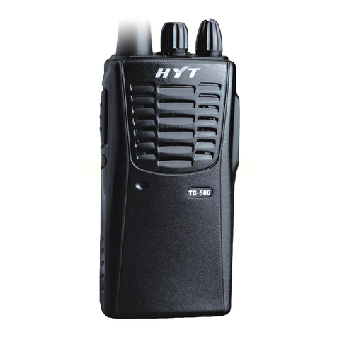
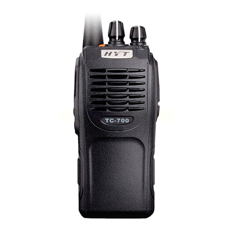
Hytera TC-508 User manual

Contents
Revision Records ---------------------------------------------------------------------------------------------------------1
Copyright Information -------------------------------------------------------------------------------------------1
Disclaimer------------------------------------------------------------------------------------------------------------------------1
Introduction-----------------------------------------------------------------------------------------------------------------------1
Radio Overview-----------------------------------------------------------------------------------------------------------------3
Software Specifications------------------------------------------------------------------------------------------------------6
Circuit Description------------------------------------------------------------------------------------------------------11
CPU Pins-------------------------------------------------------------------------------------------------------19
Part List 1---------------------------------------------------------------------------------------------------------23
Adjustment Description --------------------------------------------------------------------------------49
Troubleshooting Flow Chart--------------------------------------------------------------------------------------------58
Disassembly and Assembly-----------------------------------------------------------------------------------------------61
Exploded View------------------------------------------------------------------------------------------------------64
Part List 2--------------------------------------------------------------------------------------------------------65
PCB View-------------------------------------------------------------------------------------------------------66
Level Diagram------------------------------------------------------------------------------------------------------68
Block Diagram------------------------------------------------------------------------------------------------------69
Schematic Diagram--------------------------------------------------------------------------------------------------------70
Specifications-----------------------------------------------------------------------------------------------------------------73

TC-508 Service Manual
1
Revision History
Material No. Date of Issue Description
Initial Release
Copyright Information
Hytera and HYT are trademarks or registered trademarks of Hytera Communications Co., Ltd. (“Hytera”)
in PRC and/or other countries or areas. Hytera retains the ownership of its trademarks and product
names. All other trademarks and/or product names that may be used in this manual are properties of
their respective owners.
The Hytera product described in this manual may include Hytera computer programs stored in memory
or other media. Laws in PRC and/or other countries or areas protect the exclusive rights of Hytera with
respect to its computer programs. The purchase of this product shall not be deemed to grant, either
directly or by implication, any rights to the purchaser regarding Hytera computer programs. Any Hytera
computer programs may not be copied, modified, distributed, decompiled, or reverse-engineered in any
manner without the prior written consent of Hytera.
Disclaimer
Hytera endeavors to achieve the accuracy and completeness of this manual, but no warranty of
accuracy or reliability is given. All the specifications and designs are subject to change without prior
notice due to continuous technology development. No part of this manual may be copied, modified,
translated, or distributed in any manner without the express written permission of Hytera.
If you have any suggestions or would like to learn more details, please visit our website at:
http://www.hytera.cn.
Introduction
Manual Scope
This manual is intended for use by experienced technicians familiar with similar types of communication

TC-508 Service Manual
2
equipment. It contains all service information required for the equipment and is current as of the
publication date.

TC-508 Service Manual
3
Radio Overview
6
5
4
7
8
11
14
15
16
17
1
2
3
9
10
12
13
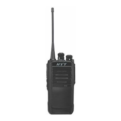
(1) PTT (Push-to-Talk)
Key (2) SK1 (programmable) (3) SK2 (programmable) (4) Antenna
(5) Channel Selector
Knob
(6) Radio On-Off/Volume
Control Knob (7) Speaker (8) Microphone
(9) LED Indicator (10) Battery Latch (11) Accessory Jack
Cover (12) Accessory Jack
(13) Strap Hole (14) Belt Clip (15) Battery (16) Screw for Belt
Clip
(17) Charging Piece

TC-508 Service Manual
4
*PTT (Push-to-Talk) Key
Press and hold down the PTT key to transmit, and release it to receive.
*SK1 and SK2
The side keys (SK1 and SK2) can be programmed with long/short press functions by your dealer.
Factory default settings are shown in the table below:
Keys Operation Function
SK1 Short press Squelch Off
Long press VOX
SK2 Short press Squelch Off
Long press Battery Strength Indicator
*Channel Selector Knob
Rotate the knob to select your desired channel.
*Radio On-Off/Volume Control Knob
Rotate the knob to turn the radio on/off or to adjust the volume.
*LED Indicator
Status indications and alert tones are shown in the table below:
Operations/Functions LED Indications and Alert Tones
User
Clone
Mode
To enter Wired Clone mode:
Turn on the source radio with SK1 held
down for approximately 2 seconds,
For the target radio, turn it on directly.
The LED on the source radio flashes red once upon
power-on.
Status of the source radio in Wired
Clone mode
(After the target radio is turned on and
the cloning cable is connected, press
PTT of the source radio to begin
cloning.)
The LED glows red during cloning process.
Error occurs during cloning:
a. User Clone Mode: Once clone begins,
frequency band and Model ID
will be checked. The Status
Indicator glows orange for 2
seconds and then goes out to
indicate a failed check. If the
check is successfully carried out
but error data clone occurs, the
Status Indicator will flash
orange. In this situation, press
any key to make it go out.
b. Factory Clone Mode: LED flashes orange
when data error occurs. Press
any key to make it go out.
The LED glows green once cloning is completed.
TC-508 Service Manual
5
Status of the target radio in Wired
Clone mode
The LED glows green during cloning process.
The green LED goes out once cloning is completed.
Power On (to enter User Mode)
When the radio is turned on, an alert tone sounds
and the Status Indicator flashes orange once.
When the radio is currently on a blank channel, it
sounds beep tone continuously.
Low Battery Alert LED flashes red, and an audio alert will be given
every 20 (programmable by your dealer) seconds.
Transmitting
The LED glows red during transmitting.
When TOT timer expires, the radio sounds beep
tones continuously.
A TOT pre-alert tone sounds before the TOT timer
expires.
Receiving The LED glows green during receiving.
Scan
The Status Indicator flashes green once per second,
while scanning is in process.
Scan Start Alert (programmable by the dealer): one
beep is heard.
Scan End Alert (programmable by your dealer): two
continuous beeps are heard.
Writing/Reading The LED glows red when reading data.
The LED glows green when writing data.
Power Adjust
A low-pitched tone is heard when the radio switches
from high power to low power.
A high-pitched tone is heard when the radio
switches from low power to high power.
VOX/Channel Lock One audio alert for enabling;
Two audio alerts for disabling;

TC-508 Service Manual
6
Software Specifications
Description
1. Channel Capacity: 16
2. Channel Spacing: 25KHz/12.5KH
3. Channel Scan
4. RX/TX status indication (red/green LED)
5. CTCSS/CDCSS (38 groups of CTCSS, 83 groups of CDCSS, and CTCSS Tail Invert by 180
degrees.)
6. Low battery alert
7. Battery Save
8. Unlock Detection and Emergency Alarm
9. 2 Selectable Squelch Levels
10. Monitor
11. Time-out Timer (TOT)
12. Squelch Tail Elimination
13. PC Programming (manual/ automatic tuning)
14. High/Low Power Switch (4.0/ 2.0W)
15. Wide & Narrow Bandwidth Compatibility
16. Busy Channel Lockout (transmission prohibited in busy status)
17. Wired Clone Mode
18. Battery Strength Indicator
19. Manual Tuning
20. VOX and 5 Selectable Sensitivity Levels
Programmable Function Keys
You dealer can assign any of the following functions to SK1 and SK2:
zNot available
zMonitor
zMonitor Momentary
zScan

TC-508 Service Manual
7
zSquelch Off
zSquelch Off Momentary
zPower Adjust
zBattery Strength Indicator
zVoice-operated Transmit (VOX)
zChannel Lock
Description of Modes
User Mode
It is a conventional communication mode. After the radio is turned on, it enters the User Mode.
PC Programming Mode
The radio in User Mode enters PC Programming Mode through specific protocol based communication
with the programming software. In this mode, radio functions and adjustment parameters can be set
through programming software (including User Version and Factory Version).
Wired Clone Mode
1. Description
Wired Clone Mode is an independent mode. To access other modes, you must restart the radio.
Wired Clone Mode includes Clone Mode and Factory Clone Mode.
1) Clone Mode:
Connect two radios using a clone cable. Hold down both SK1 and Power On/Off Key of the source
radio, it will be turned on and will enter User Clone Mode after 2 seconds. The target radio can be
directly turned on to enter user mode. In this mode, data stored in EEPROM of the source radio will
be cloned to EEPROM of the target radio. The data transferred only involves channel data and
common parameters, excluding adjustment data, version and serial No. of the model.
2) Factory Clone Mode:
Connect two radios using a clone cable. Hold down both SK1 and Power On/Off Key of the source
radio, it will be turned on and will enter User Clone Mode by default after 2 seconds. Press SK1
afterwards to switch to Factory Clone Mode. The target radio can be directly turned on to enter user
mode. The data transferred covers all data in EEPROM other than serial No, with flag of manual
tuning switch included.

TC-508 Service Manual
8
2. Process
1) The LED flashes red once after the source radio enters Wired Clone Mode. Press PTT to begin to
clone data to the target radio.
2) During cloning, LED of the source radio solidly glows red, and LED of the target radio solidly glows
green. When communication ends, the source radio glows green LED and LED of the target radio
goes out, which indicates both radios are ready for another cloning.
3) If any abnormal situation occurs during cloning, the source radio will stop cloning and its orange
LED will flash, indicating both radios are ready for another cloning.
4) When the communication ends, the source radio goes back to standby status. Press PTT again to
begin another cloning.
Manual Tune Mode
In this mode, you can manually adjust frequency deviation, power level, squelch level and etc.
See the tuning items illustrated below:
1) To enter Manual Adjust Mode
Hold down PTT and SK1 for 2 seconds while powering on the radio. The LED will glow orange when the
radio is in Tuning mode. When the keys are released, the radio will enter item N of TX group (N depends
on the position where the Channel Selector Knob locates).
(Note: This operation is subject to the option Tune Switch in the programming software.) If this option is
unchecked, the radio can not enter this mode, which helps avoid change of parameters and degradation
of radio performance caused by user’s misoperations.) Keep this option unchecked after values are well
adjusted from factory, to avoid any unexpected change of values. The adjustment values can be reset
and changed in Factory Mode only. )
2) To switch between items of TX group/RX group
This operation is done through the Channel Selector knob.
The Status Indicator glows red for adjustment of TX group items and green for adjustment of RX group
items.
3) Tuning items of TX group/Rx group
TX group items: CH1 to CH9 stand for TX Low Power, TX High Power, CDCSS Balance, CDCSS
Deviation, CTCSS Deviation (low), CTCSS Deviation (medium), CTCSS Deviation (high), TX
Low Voltage Threshold and Max. Deviation of TX Audio respectively.

TC-508 Service Manual
9
The Status Indicator solidly glows red when adjusting items CH1 to CH9.
RX Group Items: CH10-CH13 stand for SQL Normal On, SQL Normal Off, RX Low Voltage Threshold
and RX Bandpass Adjustment.
Green LED solidly glows when adjusting items CH10 to CH13.
CH14 to CH16 are unavailable and LED will go out.
4) To switch between wide and narrow bandwidth
Under a tuning item, long press PTT key to toggle between narrow band and wide band. After this
operation, the first frequency of current bandwidth is the frequency for adjustment by default.
5) To switch frequency
Short press PTT (the Status Indicator flashes green indicating valid press) to switch among different
frequencies orderly under certain bandwidth and certain adjustment item.
6) To add/subtract adjustment value
Short press SK1 under certain bandwidth and certain adjustment item to increase the adjustment value
in step of 1; hold down the key to increase the value continuously in step of 1. The adjustment value will
remain unchanged once it reaches the allowed maximum value.
Short press SK2 under certain bandwidth and certain adjustment item to decrease the adjustment value
in step of 1; hold down the key to decrease the value continuously in step of 1. The adjustment value will
remain unchanged once it reaches the allowed minimum value.
7) Operations of special items:
TX group items: CH8 represents TX Low Voltage Threshold. These adjustment items are related to AD
sampling. Press SK1 or SK2 after entering the above items, to activate AD sampling
(including calculation) once. Rotate the Channel Selector knob to save the current AD
sampling value.
Rx Group Items: CH10-CH12 stand for SQL Normal On, SQL Normal Off and Rx Low Voltage
Threshold. These tuning items are related to AD sampling. Press SK1 or SK2 after entering
the above items, to activate AD sampling (including calculation) once. Rotate the Channel
Selector knob to save the current AD sampling value.
8) Description of key-press:
Short press: key press no longer than 1 second;
Long press: key press time longer than 1 second.

TC-508 Service Manual
10

TC-508 Service Manual
11
Circuit Description
1. General Diagram
The general circuit is composed of TX section, RX section, Power Supply circuit, Control circuit and so
on. See the block diagram as shown below:
U601
MCU
SRT3210
PLL
U102
MB15E03S
L
TX/RX
VCO
Q102
POWER
MATCH ANT LPF
BPF1
BPF2
MIXER
Q502
2SK318
LNA
Q501
AT41511
DEMODULATING IC
U611
BA4116FV
IF2 FILLER
CF501
450KHz
QT_MOD
E FILLER
R103
C132
DEMODULATING
CIRCUIT
CD501,R502,
C536
MICJACK
VOX_DET
Q611
D616
R204
C204
C205
R607
R632
R206
AF AMP
U302
SW
VOLUME
S201
SW_CHANNAL
RESET IC
U605
E2ROM
U603
LDO
U604
LDO
U602
LDO
U606
V_BAT
PLL
LOOP FILTER
APC
U401
1
3
2
4
SQUELCH DET
CIRCUIT
R562
C597
BUSY
DATA/STB/CK
LD
TX_CTL
SAVE
VT
VR SW
Q604
Q305
V_SAVE
VR
SDA/SCL
RESET
EC0/EC1/EC2/EC3
MODE
AF
VOX
1
2
PTT/SK1/SK2
APC
VT
LO
QT_OUT
LO
TC-500S Block Diagram
MIC IN
CP
VR
VT
RX_TL
VCC
VDD
POWER AMP
Q403
RD07
POWER AMP
Q402
RD01
POWER AMP
Q401
2SC4226
LOCAL OSCILLATOR AMP
Q406
2SC4226
BUFFER AMP
Q105
2SC4226
LOCAL OSCILLATOR AMP
Q104
2SC5108
SW
Q405
DTC114EE
IF1 AMP
Q506
R_LED
T_LED
LED
D601
LED
D602
VDD
SPK
MODE_OUT RXD
TXD
SP_JACK
J3
PJ-D3027D
1
2
MIC
B201
QT_OUT
MODE
T/R
T/R SW
Q103
D105
QT_OUT
NOISE FILLER
CIRCUIT
R509
C553
R510 FIL IN
FIL OUT
IF1 FILLER
XF501
38.85MHz
Crystal
XT 101
38.4MHz
VR SW
D405
VT SW
D404
QT_MODULATING
FILLER
AF_MODULATING
FILLER
APC_SW
Q404
DTC114YE
APC
T/R
BATTERY
G602
5V
N-DET
AF
AF AMP
U613
TA75S01F
AF PROCESSING
CIRCUIT
U610 ,C554,R538
AF
QT-AF
AF
QT-AF
W/N
W/N
AF_SW
Q302
BEEP
BEEP
AF_MUTE
RF_MUTE
Figure 1
TX Section: The audio signal from MIC is sent to the MCU chip (U601) directly. The baseband
signal processing circuit in U601 converts the amplified audio signal to digital signal via A/D conversion,
and then converts the digital signal to analog audio signal via D/A conversion after all processing
procedures such as filtering, signal compression, pre-emphasis, TX gain control and amplitude limiting
are completed. Then the audio signal from MCU passes through the low-pass filter circuit and goes to
VCO for direct frequency modulation. The modulated HF carrier signal passes through the buffer
amplifiers (Q104 and Q406), and goes to the amplifier (Q401) through the RF switch (D404). Then the
amplified RF signal enters the low-pass filter circuit after it is further amplified by the pre-driver (Q402)
and final-stage power amplifier (Q403), and then it will be finally transmitted via antenna after ultra
harmonics is removed.

TC-508 Service Manual
12
RX Section: RF signals received via the antenna are fed to the band-pass filter to filter out undesired
out-of-band interference signal. Then the remaining RF signals are amplified by LNA Q501. Afterwards,
the amplified signal goes through the bandpass filter again to filter out undesired out-of-band
interference signal. Next, the RF signals will be mixed with the first local oscillator signal at Q502. Then
the newly generated signals will be processed by crystal filter XF501 to produce 38.85M the first IF
signal. After being amplified, the IF signal goes via Q506 to the chip U611, where the IF signal will be
mixed with the second local oscillator for the second time to produce the 450KHz second IF signal. After
filtered by 450KHZ ceramic filter, U611 demodulates the IF signal to output audio signal, which will be
delivered to Q613 for amplification and output in two channels. After simple filtering, one of the channels
is fed to MCU U601 for CTCSS/CDCSS decoding; for the other channel, it will go through two stages of
low-pass filter first, and then it goes to high-pass filter (consisting of 4 operational amplifiers) for audio
processing. Finally, the signals will be sent to audio power amplifier U302 for amplification so as to drive
the speaker.
Power Supply Section: the 7.4V battery voltage is converted to 5V via DC-DC module U604, and
further converted via LDO U602 to 3V including two channels: VCC and VDD. VCC powers CPU and
VDD powers PLL circuit. The 5V voltage will be converted via LDO U606 to 4.5V including two channels:
VT and V-SAVE. V-SAVE powers VCO circuit and VT powers TX circuit. Finally, V-SAVE together Q604
and Q305 are used to control VR, which powers RX circuit.
2. Realization Methods of Basic Functional Modules
2.1 PLL Frequency Synthesizer
The PLL circuit mainly provides the local oscillator signal for RX and RF carrier signal for
TX. It is composed of VCO and PLL chip, allowing frequency tracking and channel switching
under the control of MCU signals.
1) PLL

TC-508 Service Manual
13
U601
MCU
SRT3210
TX/RX
VCO
Q102
QT_MODE
FILLER
R103
C132
PLL
LOOP FILTER
1
3
2
4
DATA/STB/CK
LD
QT_OUT
CP
BUFFER AMP
Q105
2SC4226
LOCAL OSCILLATOR AMP
Q104
2SC5108
VDD
MODE
T/R SW
Q103
D105
Crystal
XT 101
38.4MHz
T/R
PLL
U102
MB15E03SL
Figure 2
The PLL circuit generates RF carrier signal for TX and the first local oscillator signal for
RX.
Step frequency of PLL circuit is 6.25 KHz and 5 KHz. In U101, the 38.4MHz reference oscillator
signal is divided into 5 KHz and 6.25 KHz reference frequencies via a fixed counter in PLL. The signal
from VCO (TX/RX VCO) enters the PLL after processed by the buffer amplifier. In the PLL, the signal is
processed by a variable frequency divider. After division, the signal is compared with the reference
frequency in a phase detector (PD) of the PLL. The signal from the PD passes through a low-pass filter
and then is sent to the varactors (D101 and D102) of VCO to control the output frequency. Then the RF
signal is processed by the buffer amplifiers (Q104 and Q406), and controlled by D616 and D617 to only
serve as TX signal or RX first local oscillator signal.
2) VCO
VCO section is realized by the oscillator circuit of three-point capacitance. TX VCO and RX VCO
share the same oscillator circuit. The TX/RX VCO is controlled by Q103.
Note: If the PLL is unlocked, the LD pin of U101 outputs low level. If the microprocessor detects
such situation, TX/RX operation is prohibited, and an alarm sounds.
2.2 RF Power Amplifier Circuit (TX Section)
The block diagram of the RF power amplifier circuit is shown in the figure below:

TC-508 Service Manual
14
TX/RX
VCO
Q102
POWER
MATCH ANT LPF
APC
U401
VT
LO
VT
POWER AMP
Q403
RD07
POWER AMP
Q402
RD01
POWER AMP
Q401
2SC4226
LOCAL OSCILLATOR AMP
Q104
2SC5108
SW
Q405
DTC114EE
T/R SW
Q103
D105
VR SW
D405
VT SW
D404
APC_SW
Q404
DTC114YE
APC
T/R
LOCAL OSCILLATOR AMP
Q406
2SC4226
Figure 3
The modulated carrier signal from VCO is pre-amplified at Q104 and Q406, and controlled at D404
and D405. Then it is amplified by the front-stage amplifier Q401, the pre-driver Q402 and the final-stage
amplifier Q403 orderly. Finally it will be transmitted via antenna after ultra harmonics are removed by the
LC low-pass filter circuit.
APC circuit is composed of Q404, Q405 and U401. U401 controls the bias voltage at the gates of
Q402 and Q403, to control TX current and to further regulate power.
2.3 RX LNA and Mixer Circuit (RX Section)
The Block Diagram of RX Circuit is shown as below:

TC-508 Service Manual
15
BUSY
LO
AF
Figure 4
RF signals received via the antenna are fed to the band-pass filter to filter out undesired out-of-band
interference signal. Then the remaining RF signals are amplified by LNA Q501. Afterwards, the amplified
signal goes through the bandpass filter again to filter out undesired out-of-band interference signal. After
being filtered and amplified, the RF signals and first LO signals are mixed at Q502, and then the mixed
signal is filtered by crystal filter XF501 to get 38.85MHz differential signals as the first IF signal.
After being amplified by Q506, the IF signal goes to chip U608, where the signal will be mixed with
the second LO signal (38.4MHZ). Next, the signals will be filtered by CF501 to produce 450 KHz IF
signal. When the IF signals are processed by demodulation circuit (including U611 and CD501) to
generate audio signals, which are delivered to IC Q613 for amplification and output in two channels.
After simple filtering, one channel of signals is supplied to MCU U601 for CTCSS/CDCSS decoding; for
the other channel, it will go through two stages of low-pass filter first, and then it goes to high-pass filter
U610 (consisting of 4 operational amplifiers) for audio processing. Finally, the signals will be sent to
audio power amplifier U302 for amplification so as to drive the speaker.
2.4 MCU Control, Signal Processing and Audio Power Amplification
Circuit diagram of this section is shown as below:

TC-508 Service Manual
16
Figure 5
1) MCU Control Circuit
MCU control circuit is composed of MCU, EEPROM, keys and etc. This section has the following
functions: to initialize data of the radio and save data to EEPROM; to detect battery voltage and signals
from external keys, LD and VOX, and to make response; to transmit required data to PLL based on the
channel encoding status; to switch and control RX/TX based on the input PTT signal; to switch the
squelch circuit on/off based on the input signaling decode signal and squelch level signal; to control
circuits of high/low power switch, audio power amplifier, VCO power supply, RX power supply and TX
power supply; (for programming) to communicate with PC via RXD/TXD based on the RS232 protocol,

TC-508 Service Manual
17
and transmit/receive data to/from PC.
2) Signal Processing Circuit
a. TX Baseband Processing
The audio signals input from MIC are divided into two parts. One part enters U601, and is then
converted into digital signal by analog-to-digital conversion (ADC). Afterwards, the converted signal will
go through a series of processing including low-pass filtering, AGC, companding, high-pass filtering, and
pre-emphasizing, and then it will be output as baseband signal after digital-to-analog conversion (DAC).
The baseband signal is processed by the active low-pass filter and then sent to VCO for modulation; for
the other part, it will go through VOX circuit (Q611 and D616) and then sent to MCU for VOX processing.
b. RX Baseband Processing
The demodulated IF signals with CTCSS/CDCSS signaling enter U601 for decoding. After ADC, the
IF signals will be converted into digital signals, which go to low-pass filter for filtering and then are
divided into two parts. One part is processed by CTCSS/CDCSS decoder, and the other is processed by
high-pass filter and then is subject to de-emphasis, decryption, signal expansion and DTMF
demodulation and etc, and finally digital-to-analog conversion to output audio signal.
3) Audio Amplifier
The audio signal output from U601 is amplified by the audio power amplifier (U302) to drive the
speaker directly.
2.5 Power Supply Processing
Block diagram of power supply circuit is shown as below:

TC-508 Service Manual
18
LDO
U604
LDO
U602
LDO
U606
V_BAT
TX_CTL
SAVE
VT
VR SW
Q604
Q305
V_SAVE
VR
VCC
VDD
5V
RF_MUTE
Figure 6
Power Supply Section: the 7.4V battery voltage is converted to 5V via DC-DC module U604, and further
converted via LDO U602 to 3V including two channels: VCC and VDD. VCC powers CPU and VDD
powers PLL circuit. The 5V voltage will be converted via LDO U606 to 4.5V including two channels: VT
and V-SAVE. V-SAVE powers VCO circuit and VT powers TX circuit. Finally, V-SAVE together Q604 and
Q305 are used to control VR, which powers RX circuit.

TC-508 Service Manual
19
CPU Pins
Pin
No. Port Name Pin Name I/O Function
1 NC / / /
2 NC / / /
3 NC / / /
4 NC / / /
5 NC / / /
6 TXD TXD O UART TX
7 RXD RXD I UART Red
8 P60 APA_EN O Control speaker (H: unmute; L: mute)
9 P61 SAVE_CTL O Control Power Save; in non-Power-Save
status, it is at high level.
10 P62 EXT MIC I Check MIC connection (valid for high level)
11 P63 EXT PTT I PTT key on the earpiece (valid for high level)
12 P64 Red LED O Red LED indicator
13 P65 Green LED O Green LED indicator
14 P66 R/T O RX/TX control (H: RX; L: TX) (switch to VCO)
15 P67 RX_CTRL O Control power supply for RX (receive at high
level)
16 Vssd GND S Ground power supply for digital circuit
17 Vddd VCC(3.0V)S Power supply for digital circuit
18 P50/INT0 Reserve O Reserved
19 P51/INT1 Reserve O Reserved
20 P52/INT2 Reserve O Reserved
21 P53/INT3 SK2 I Side key2 (programmable) (valid at low level)
22 P54/INT4 SK1 I Side key 1 (programmable) (valid at low level)
23 P55/INT5 PTT I PTT key (valid for low level)
24 P56/INT6 Reserve O Reserved
25 P57/INT7 Reserve O Reserved
26 Vdd_CLD
VCC(3.0V)S Power supply for digital PA
27 CLD_OUTP CLD_OUTP O Positive output of digital PA
Other manuals for TC-508
2
Table of contents
Other Hytera Two-way Radio manuals

Hytera
Hytera AP58X User manual

Hytera
Hytera PD40X User manual

Hytera
Hytera PD752 User manual

Hytera
Hytera PNC370 User manual

Hytera
Hytera PD365 User manual

Hytera
Hytera PT790 User manual

Hytera
Hytera TETRA User manual

Hytera
Hytera TC-780 VHF User manual

Hytera
Hytera PT580 User manual

Hytera
Hytera X1p Service manual

Hytera
Hytera X1e User manual

Hytera
Hytera TC-508V2 User manual

Hytera
Hytera TM-600 User manual

Hytera
Hytera PD782 User manual

Hytera
Hytera AP51X User manual

Hytera
Hytera X1p User manual

Hytera
Hytera PD405 User manual

Hytera
Hytera HYT TC-500 User manual

Hytera
Hytera TC-700 User manual

Hytera
Hytera PT350 User manual