TC-500ServiceManual
- 8 -
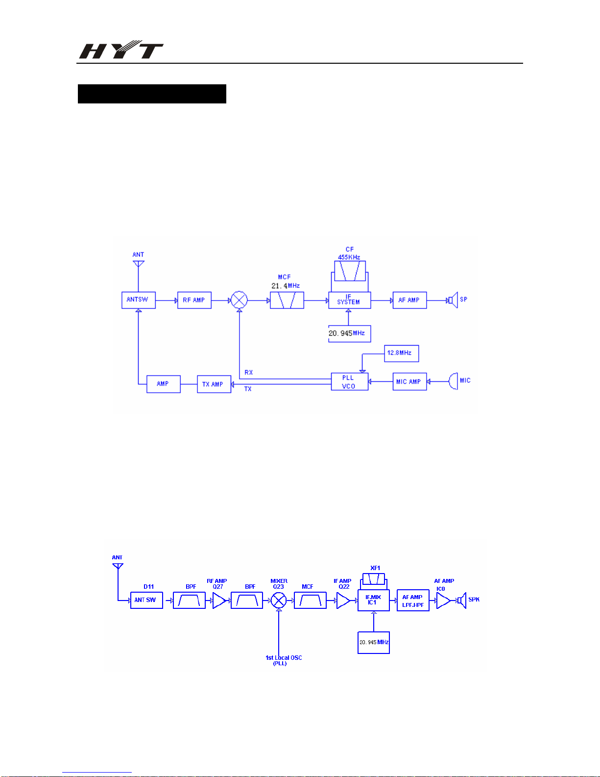
Initial data table
Note: For standard model, CTCSS is off in all channels after initialization.
1CH(Center) 2CH(Low) 3CH(High) 4CH 5CH 6CH 7CH 8CH 9-16CHMS1 Model
Frequency (MHz) IF (MHz) Tx
(MHz)
Rx
(MHz)
Tx
(MHz)
Rx
(MHz)
Tx
(MHz)
Rx
(MHz)
(MHz)
(MHz)
(MHz)
(MHz)
(MHz)
(MHz)
0 1 150.000~173.995 +21.4 162.000 162.100 150.000 150.100 173.975 173.900 162.500 162.550 162.600 162.550 162.650
0 2 136.000~149.995 +21.4 143.000 143.100 136.000 136.100 149.975 149.900 143.500 143.550 143.600 143.550 143.650
0 3 146.000~173.995 +21.4 160.000 160.100 146.000 146.100 173.975 173.900 160.500 160.550 160.600 160.550 160.650
0 4 144.000~147.995 +21.4 146.000 146.100 144.000 144.100 147.975 147.900 146.500 146.550 146.600 146.550 146.650
0 5 136.000~147.995 +21.4 142.000 142.100 136.000 136.100 147.975 147.900 142.500 142.550 142.600 142.550 142.650
0 6 136.000~173.995 +21.4 155.000 155.100 136.000 136.100 173.975 173.900 155.500 155.550 155.600 155.550 155.650
0 7 450.000~469.995 -21.4 460.000 460.100 450.000 450.100 469.975 469.900 460.300 460.350 460.400 460.350 460.450
0 8 400.000~419.995 -21.4 410.000 410.100 400.000 400.100 419.975 419.900 410.500 410.550 410.600 410.550 410.650
0 9 470.000~489.995 -21.4 480.000 480.100 470.000 470.100 489.975 489.900 480.500 480.550 480.600 480.550 480.650
0 10 490.000~511.995 -21.4 501.000 501.100 490.000 490.100 511.975 511.900 501.500 501.550 501.600 501.550 501.650
0 11 220.000~239.995 -21.4 230.000 230.100 220.000 220.100 239.975 239.900 230.500 230.550 230.600 230.550 230.650
1 1 240.000~259.995 -21.4 250.000 250.100 240.000 240.100 259.975 259.900 250.500 250.550 250.600 250.550 250.650
1 2 336.000~367.995 -21.4 352.000 352.100 336.000 336.100 367.975 367.900 352.500 352.550 352.600 352.550 352.650
1 3 368.000~395.995 -21.4 382.000 382.100 368.000 368.100 395.975 395.900 382.500 382.550 382.600 382.550 382.650
1 4 370.000~389.995 -21.4 380.000 380.100 370.000 370.100 389.975 389.900 380.500 380.550 380.600 380.550 380.650
1 5 350.000~369.995 -21.4 360.000 360.100 350.000 350.100 369.975 369.900 360.500 360.550 360.600 360.550 360.650
1 6 406.000~429.995 -21.4 418.000 418.100 406.000 406.100 429.975 429.900 418.500 418.550 418.600 418.550 418.650
1 7 400.000~429.995 -21.4 415.000 415.100 400.000 400.100 429.975 429.900 415.500 415.550 415.600 415.550 415.650
1 8 430.000~439.995 -21.4 435.000 435.100 430.000 430.100 439.975 439.900 435.500 435.550 435.600 435.550 435.650
1 9 438.000~449.995 -21.4 444.000 444.100 438.000 438.100 449.975 449.900 444.500 444.550 444.600 444.550 444.650
1 10 480.000~519.995 -21.4 500.000 500.100 480.000 480.100 519.975 519.900 500.500 500.550 500.600 500.550 500.650
1 11 441.000~451.000 -21.4 446.000 446.100 441.000 441.100 450.975 450.900 446.500 446.550 446.600 446.550 446.650
Standard 446.00625~446.09375 -21.4 446.00625 446.00625 446.01875 446.01875 446.03125 446.03125 446.04375 446.05625 446.06875 446.08125 446.09375
CH QT/DQT OFF OFF OFF OFF OFF OFF OFF 023 023 127.3 151.4