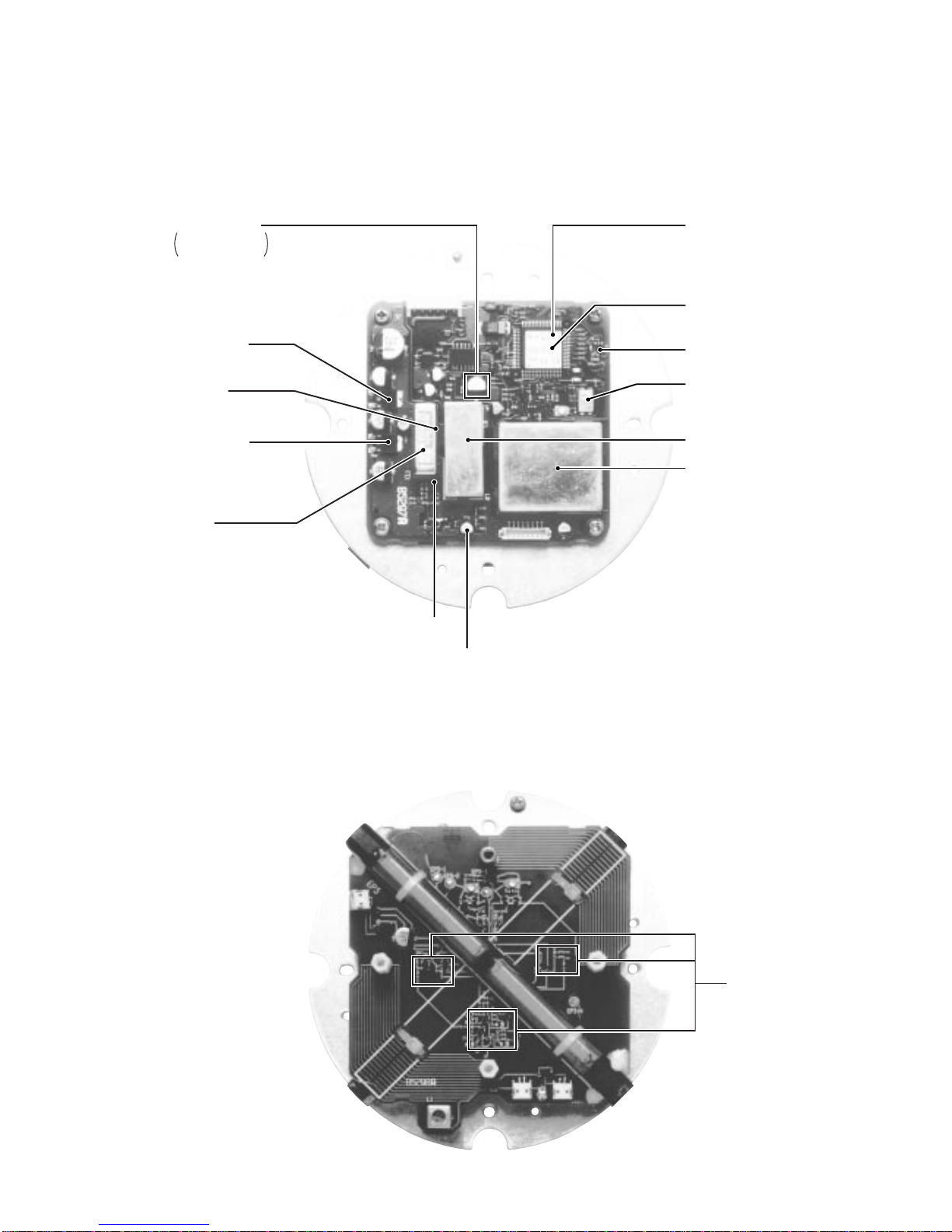
Icom FP-561 User manual

SERVICE
MANUAL
6-9-16, Kamihigashi, Hirano-ku, Osaka, 547-0002, Japan S-13602II-CD
© 1999 Icom Inc.
MARINE PLOTTER/SOUNDER
DGPS BEACON RECEIVER
COVER 99.11.24 9:24 AM Page 1

6-9-16, Kamihigashi, Hirano-ku, Osaka 547-0002, Japan
Phone : 06 6793 5302
Fax : 06 6793 0013
Communication Equipment
Himmelgeister Str. 100, D-40225 Düsseldorf, Germany
Phone: 0211 346047 Fax : 0211 333639
URL : http://www.icomeurope.com
Unit 9, Sea St., Herne Bay, Kent, CT6 8LD, U.K.
Phone: 01227 741741 Fax : 01227 741742
URL : http://www.icomuk.co.uk
Zac de la Plaine, Rue Brindejonc des Moulinais
BP 5804, 31505 Toulouse Cedex, France
Phone: 561 36 03 03 Fax : 561 36 03 00
URL : http://www.icom-france.com
Crta. de Gracia a Manresa Km. 14,750
08190 Sant Cugat del Valles Barcelona, SPAIN
Phone: (93)590 26 70 Fax : (93)589 04 46
URL : http://www.icomspain.com
<
Corporate Headquarters
>
2380 116th Avenue N.E., Bellevue, WA 98004, U.S.A.
Phone: (425)454-8155 Fax : (425)454-1509
URL : http://www.icomamerica.com
<
Customer Service
>
Phone: (425)454-7619
A.C.N. 006 092 575
290-294 Albert Street, Brunswick, Victoria, 3056, Australia
Phone: 03 9387 0666 Fax : 03 9387 0022
URL : http://www.icom.net.au
6F No. 68, Sec. 1 Cheng-Teh Road, Taipei, Taiwan, R.O.C.
Phone: (02) 2559 1899 Fax : (02) 2559 1874
3071 #5 Road, Unit 9, Richmond, B.C., V6X 2T4, Canada
Phone: (604)273-7400 Fax : (604)273-1900
URL : http://www.icomcanada.com
INTRODUCTION
DANGER
ORDERING PARTS
REPAIR NOTES
This service manual describes the latest service information
for the FP-561 MARINE PLOTTER/SOUNDER and RD-200
DGPS BEACON RECEIVER at the time of publication.
To upgrade quality, all electrical or mechanical parts and
internal circuits are subject to change without notice or
obligation.
VERSION
MODEL
FP-561 General
Europe
SYMBOL
GEN
EUR
NEVER connect the unit to an AC outlet or to a DC power
supply that uses more than 33 V (FP-561) or 16 V (RD-200).
Such a connection could cause a fire hazard and/or electric.
DO NOT expose the unit to rain, snow or any liquids.
DO NOT reverse the polarities of the power supply when
connecting the unit.
DO NOT apply an RF signal of more than 20 dBm (100mW)
to the antenna connector. This could damage the unit’s front
end.
Be sure to include the following four points when ordering
replacement parts:
1. 10-digit order numbers
2. Component part number and name
3. Equipment model name and unit name
4. Quantity required
<SAMPLE ORDER>
0910051392 PCB B-5305 FP-561 MAIN UNIT 1 pieces
8810004540 Screw BiH 3x8 SUS FP-561 Chassis 10 pieces
Addresses are provided on the inside back cover for your
convenience.
1. Make sure a problem is internal before disassembling
the unit.
2. DO NOT open the unit until the unit is disconnected from
its power source.
3. DO NOT force any of the variable components. Turn
them slowly and smoothly.
4. DO NOT short any circuits or electronic parts. An insulat-
ed turning tool MUST be used for all adjustments.
5. DO NOT keep power ON for a long time when the unit is
defective.
6. READ the instructions of test equipment thoroughly
before connecting equipment to the unit.
FP-561 RD-200
COVER 99.11.24 9:24 AM Page 2

TABLE OF CONTENTS
SECTION 1 SPECIFICATIONS
1-1 FP-561 . . . . . . . . . . . . . . . . . . . . . . . . . . . . . . . . . . . . . . . . . . . . . . . . . . . . . . . . . . . . . . . . .1-1
1-2 RD-200 . . . . . . . . . . . . . . . . . . . . . . . . . . . . . . . . . . . . . . . . . . . . . . . . . . . . . . . . . . . . . . . .1-2
SECTION 2 INSIDE VIEWS
2-1 FP-561 . . . . . . . . . . . . . . . . . . . . . . . . . . . . . . . . . . . . . . . . . . . . . . . . . . . . . . . . . . . . . . . . .2-1
2-2 RD-200 . . . . . . . . . . . . . . . . . . . . . . . . . . . . . . . . . . . . . . . . . . . . . . . . . . . . . . . . . . . . . . . .2-2
SECTION 3 CIRCUIT DESCRIPTION
3-1 TRANSMITTER CIRCUITS . . . . . . . . . . . . . . . . . . . . . . . . . . . . . . . . . . . . . . . . . . . . . . . . .3-1
3-2 RECEIVER CIRCUITS . . . . . . . . . . . . . . . . . . . . . . . . . . . . . . . . . . . . . . . . . . . . . . . . . . . . .3-1
3-3 REGULATOR CIRCUITS . . . . . . . . . . . . . . . . . . . . . . . . . . . . . . . . . . . . . . . . . . . . . . . . . . .3-2
3-4 INTERFACE CIRCUITS . . . . . . . . . . . . . . . . . . . . . . . . . . . . . . . . . . . . . . . . . . . . . . . . . . . .3-3
3-5 LOGIC CIRCUITS . . . . . . . . . . . . . . . . . . . . . . . . . . . . . . . . . . . . . . . . . . . . . . . . . . . . . . . .3-3
3-6 DGPS RECEIVER . . . . . . . . . . . . . . . . . . . . . . . . . . . . . . . . . . . . . . . . . . . . . . . . . . . . . . . .3-4
3-7 PORT ALLOCATIONS . . . . . . . . . . . . . . . . . . . . . . . . . . . . . . . . . . . . . . . . . . . . . . . . . . . . .3-5
SECTION 4 ADJUSTMENT PROCEDURES
4-1 PREPARATION . . . . . . . . . . . . . . . . . . . . . . . . . . . . . . . . . . . . . . . . . . . . . . . . . . . . . . . . . .4-1
4-2 FP-561 TRANSMITTER ADJUSTMENT . . . . . . . . . . . . . . . . . . . . . . . . . . . . . . . . . . . . . . . .4-2
4-3 FP-561 RECEIVER ADJUSTMENT . . . . . . . . . . . . . . . . . . . . . . . . . . . . . . . . . . . . . . . . . . .4-2
4-4 FP-561 WATER TEMPERTUREM ADJUSTMENT . . . . . . . . . . . . . . . . . . . . . . . . . . . . . . . .4-2
4-5 RD-200 ADJUSTMENTS . . . . . . . . . . . . . . . . . . . . . . . . . . . . . . . . . . . . . . . . . . . . . . . . . . .4-4
SECTION 5 PARTS LIST
SECTION 6 MECHANICAL PARTS AND DISASSEMBLY
SECTION 7 SEMI-CONDUCTOR INFORMATION
SECTION 8 BOARD LAYOUTS
8-1 FP-561
8-1-1 SW UNIT . . . . . . . . . . . . . . . . . . . . . . . . . . . . . . . . . . . . . . . . . . . . . . . . . . . . . . . . . . . .8-1
8-1-2 LOGIC UNIT . . . . . . . . . . . . . . . . . . . . . . . . . . . . . . . . . . . . . . . . . . . . . . . . . . . . . . . . .8-3
8-1-3 MAIN UNIT . . . . . . . . . . . . . . . . . . . . . . . . . . . . . . . . . . . . . . . . . . . . . . . . . . . . . . . . . .8-5
8-2 RD-200
8-2-1 MAIN UNIT . . . . . . . . . . . . . . . . . . . . . . . . . . . . . . . . . . . . . . . . . . . . . . . . . . . . . . . . . .8-7
8-2-2 ANT UNIT . . . . . . . . . . . . . . . . . . . . . . . . . . . . . . . . . . . . . . . . . . . . . . . . . . . . . . . . . . .8-9
SECTION 9 BLOCK DIAGRAM
9-1 FP-561 . . . . . . . . . . . . . . . . . . . . . . . . . . . . . . . . . . . . . . . . . . . . . . . . . . . . . . . . . . . . . . . . .9-1
9-2 RD-200 . . . . . . . . . . . . . . . . . . . . . . . . . . . . . . . . . . . . . . . . . . . . . . . . . . . . . . . . . . . . . . . .9-2
SECTION 10 VOLTAGE DIAGRAM
10-1 FP-561 . . . . . . . . . . . . . . . . . . . . . . . . . . . . . . . . . . . . . . . . . . . . . . . . . . . . . . . . . . . . . . . . .10-1
10-2 RD-200 . . . . . . . . . . . . . . . . . . . . . . . . . . . . . . . . . . . . . . . . . . . . . . . . . . . . . . . . . . . . . . . .10-3

1-1 FP-561
‘GENERAL
• Display : 5.6 inch TFT color LCD (320×234 pixels)
•Power supply requirement : 11–30 V DC
•LCD brightness : 16 levels
•Power consumption : Less than 22 W (Less than 1.8 A at 12 V DC)
•Dimensions (projections not included) : 186(W)×203(H)×102(D) mm; 75⁄16(W)×8(H)×4(D) in
•Weight (approx.) : 2.2 kg; 4 lb 14 oz
•Usable temperature range : 0˚C to +50˚C; +32˚F to +122˚F
•Unit of water depth : m (meter), FT (feet), FM (fathom)
•Unit of water temperature : ˚C, ˚F
•Unit of speed : KT (knots), km/h, MI/h (miles/h)
•Unit of distance : NM (nautical miles), km, MI (miles)
•Input data format : NMEA0183, Water temp./speed, DGPS
•Output data format : NMEA0183 (GGA, GLL, XTE, AAM, VTG, BOD, WPL, BWC),
Start-stop serial forward; 4800 bps
‘GPS
•Receive system : 12 parallel-channel, all-in-one view
•Receive frequency : 1575.42 MHz (±1 MHz)
•Measuring accuracy (2DRMS) : Position 100 m, 95% of the time, PDOP≤3 (Less than 100 m, S/A OFF)
Speed Less than 1 m/sec. (PDOP≤3, S/A ON)
NOTE: All GPS receivers are subject to degradation of position and velocity accuracy under the U.S. Department of
Defence.
•Data renewed interval : 1 sec.
‘PLOTTER
•Scale setting : 16 steps
•Plotting interval : 5 sec. to 60 min., 0.01–9.99 NM*
•No. of track memories : 5000 (selectable from 7 colors)
•No. of route memories : 20 (50 points/route)
•No. of event markers : 500
•Navigation computer : Vessel position (longitude/latitude), cursor position, distance, elapsed time,
course-out distance, direction, distance, time
•Data indication : Coastline, place name, contour line, route, lighthouse, longitude/latitude line
•Alarm : Area and Arrival alarms
1 - 1
SECTION 1 SPECIFICATIONS

1 - 2
All stated specifications are subject to change without notice or obligation.
‘VIDEO SOUNDER
•Transmission freq. : 50 kHz, 200 kHz
•Output power : 500 W RMS
•Water depth range : 5–640 m* in 8-color indication
•Water temp. range : 0˚C to +40˚C; +32˚F to +104˚F
•Speed range : 0.0–99.9 KT*
•Bottom lock expansion range : 5 m*, 10 m*, 20 m*, 40 m*
•Phase shift variable range : 1–640 m*
•Type of display screen : Standard, A-scope, dual frequencies, bottom and marker zoom
•Picture sweep speed : 6 levels including pause
•Alarm : Shallow, depth and fish school
*selectable in each unit
1-2 RD-200
‘GENERAL
•Frequency coverage : 283.5 kHz to 325.0 kHz
•Type of emmision : 1K0F2B
•Antenna impedance : 50 Ωnominal
•Intermediate frequency : 455 kHz
•Usable temperature range : –20˚C to +70˚C; –4˚F to +158˚F
•Power supply requirement : 12 V DC nominal negative ground
•Current drain (at 12 V DC) : Less than 0.2 A
•Dimensions (projections not included) : 140(d)×157.2(H) mm; 51⁄2(d)×63⁄16(H) in
•Weight : 1.0 kg; 2 lb 3 oz
‘RECEIVER
•Intermediate frequency : 455 kHz
•Sensitivity : 0.2 µV at 12 dB SINAD
•Sprious response : 60 dB
•Intermodulation : 50 dB

2 - 1
SECTION 2 INSIDE VIEWS
2-1 FP-561
• MAIN UNIT
• LOGIC UNIT
+5V regulator
(IC13: PQ05RF21)
GPS receiver
Switching control
(IC9: UPC494GS)
12V rectifier
(D13: SB30-09J)
8V rectifier
(D22: SB30-09J)
+6V regulator
Q27: 2SD1664 Q
D37: RD7.5M B1
40V rectifier
(D12: RG-2A)
Power amplifier
Q6, Q7: FS30KMJ-3
Q23, Q24: 2SC3326-B
Driver
IC2: TC4093BF
Q2, Q3: 2SC2712-GR
Q4, Q5: 2SA1162-GR
STC circuit
Q1: 2SC3326-B
Q26: 2SC2712-GR
200 kHz local oscillator circuit
IC3: TC3W03FU
X1: CR-497 (5.24MHz)
50 kHz local oscillator circuit
IC4: TC3W03FU
X2: CR-496 (4.04MHz)
Crystal oscillator
(X1: DSO-49SJ)
Main CPU
(IC1: CL-PS7500FE)
FIFO RAM
(IC20: CY7C433-40JC)
DRAM
(IC34, IC35: M5M44260CJ) SRAM
(IC30, IC31: M5M51008BVP-70LL)
Flash ROM
(IC32, IC33: MBM29F800BA-90PFTN)
Sub CPU
(IC22: TMP90PM36F)
Mail box RAM
(IC21: M66220FP)
DC-DC converter
Q4: 2SB120IS
Q5: XP6501AB

2 - 2
2-2 RD-200
• MAIN UNIT
• ANT UNIT
DDS
(IC6: SC-1287)
1st mixer
(IC2: ND487C1 3R)
CPU
(IC12: HD64F3644H)
EEPROM*
(IC13: X25320SI-2.7)
D/A converter
(IC19: TA75S01F)
Reference oscillator
(X1: DSX751S 14.5984MHz)
+5V regulator
(IC9: TA7805F)
IF filter
(FI1: CFJ455K8)
IF amplifier*
(Q1: 3SK131 K)
RF amplifier*
(IC1: µPC1676G)
* : Located under side of these point
+8V regulator
(IC8: TA7808F)
FM IF IC*
(IC3: TA31136FN (D))
+6.5V regulator*
Q3: 2SD1664 Q
D2: MA8075 L
RF amplifier
(Q1– Q8: 2SK209 GR)

3 - 1
SECTION 3 CIRCUIT DESCRIPTION
3-1 TRANSMITTER CIRCUITS
3-1-1 TRANSMIT OUTPUT PULSE CONTROL
CIRCUIT
The 200 kHz/50 kHz pulse signals from the LOGIC unit via
J1 (pin 3) are passed through the buffer amplifier circuit (IC1,
pin 1 and pin 3), and are inverted and output from IC1 (pin 2
and pin 5) as 180˚phase difference pulse signals.
The signals from the buffer amplifier are passed through the
integrate circuits (D1, R2, C3 and D2, R3, C4) which adjust
switching time for tuning ON Q6, Q7 separately to prevent
overlap of output pulses (200 kHz and 50 kHz). The integrate
circuits change the pulse signals which characteristics of 50
% duty-cycle to slow switching time for leading and leave
quick switching time for trailing.
The pulse signals are applied to the Schmitt NAND gates
(IC2, pins 1 and 5). Also trasmit triger signal from the LOGIC
unit is applied to IC2 (pins 2 and 6) via C86. Only when both
signals are input, IC2 outputs transmit signals from pin 11 or
pin 10.
3-1-2 TRANSMITTER OUTPUT CIRCUIT
The transmitter output circuit consists of the driver and out-
put circuits.
The driver circuit consists of Q2–Q5. The Darlington connec-
tion, used for switching circuits, consists of a pair of transis-
tors for Q2 and Q4, and for Q3 and Q5. This is because the
next circuit which consists of FETs requires quick switching
time for leading and trailing characteristics.
The output circuit consists of Q6, Q7 and T1. When no trans-
mission is occurring, transmit power is charged into C28 and
energy outputs at the next moment by turning ON Q6 or Q7.
3-1-3 OUTPUT POWER CIRCUIT
This circuit consists of IC10, Q11, Q12 and Q13. A signal
from the LOGIC unit controls voltage to be applied to the pri-
mary winding of T1 through these components.
3-1-4 DIODE ISOLATION CIRCUIT
D3, D30, D4, D31, D9, D32, D35, D36 are symmetry-type sil-
licon-varister diodes. Interior connection is simulated as
shown in the diagram (Fig.1).
Fig.2 shows the diode’s electronic characteristics. When the
voltage is +Vd or less, internal resistance is infinitie. This
condition is the same as when a diode is OFF. when the volt-
age exceeds +Vd, internal resistance for each diode is at its
minimum level. This condition is the same as when a diode
is turned ON.
When transmitting, high voltage is applied to the circuit and
when receiving, no voltage is applied. Therefore, the receiv-
er circuit is protected from high power transmit signals when
transmitting, and the receiver circuit is isolated from the
transmitter circuit when receiving.
3-2 RECEIVER CIRCUITS
3-2-1 RECEIVER MATCHING CIRCUIT
The matching circuits for the 200 kHz signal and for the 50
kHz signal consist of L1, C93 and L6, C96 respectively. The
tuned signals at each matching circuit are applied to the ana-
log switch (IC16).
The analog switch (IC6) switches received signals by the Rx
frequency control signal (LOCONT) from LOGIC unit via J5
(pin 5), and then outputs to the next stage which is the mixer
circuit.
When transmit/receive 200 kHz signal, LOCONT is low level
and pin 7 (IC16) is ON. Therefore, IC16 (pin 1) outputs tuned
200 kHz signal.
When transmit/receive 50 kHz signal, LOCONT is high level
and pin 6 (IC16) is ON. Therefore, IC16 (pin 1) outputs tuned
50 kHz signal.
I
I
V
V
+Vd
–Vd
Fig.1 Fig.2
• DIODE ISOLATION CIRCUIT

3 - 2
3-2-2 STC CIRCUIT
The STC circuit (Q1, R115, Q26, R116, C102) reduces the
sensitivity near-by the dispach line to set the immunity to air
bubbles in the sea surfaces so as to improve the image leg-
ibility.
When transmitting, the Tx trigger signal (TXTRG) from
LOGIC unit via J5 (pin 4) is high level, at this time Q26 is ON
and then Q1 turns ON. When switching TX to RX, the Tx trig-
ger signal (TXTRG) becomes low level and Q26 is OFF, and
then Q1 turns to OFF slowly by connecting time constant
(R116, C102).
Thus the STC function activates.
3-2-3 MIXER AND DETECTOR CIRCUITS
The mixer circuit converts the received signals into the 455
kHz IF signal.
The FM IF IC (IC5) contains the mixer, 455 kHz IF amplifier
and RSSI circuits.
The 200 kHz/50 kHz signals from the STC circuit (Q1) are
applied to the mixer section of IC5 (pin 16), and are mixed
with the 655 kHz/505 kHz LO signals generated at the 200
kHz/50 kHz local oscillator circuits to produce a 455 kHz IF
signal.
The 455 kHz IF signal from IC5 (pin 3) passes through the
ceramic filter (FI1), where unwanted signals are suppressed,
and is then applied to the IF amplifier section in IC5 (pin 5).
IC5 (pin 12) outputs RSSI voltage accoding to the input level
of IF amplifier section. The RSSI voltage is amplified at the
DC amplifier (IC6) to obtain necessary level, and is then
applied to the LOGIC unit.
The RSSI control signal from the LOGIC unit via J1 (pin 13)
becomes high level when the received signal is deeper than
80 m. Then the signal reduces noise by turning ON Q25 to
connect the by-pass capacitor (C90).
3-2-5 LOCAL OSCILLATOR CIRCUITS
200 kHz/50 kHz local oscillator circuits consist of IC3, X1 and
IC4, X2 respectively. IC3 or IC4 includes a frequency divider.
When high level signal is applied to pin 1, IC3 or IC4 oscil-
lates and divides frequency, when low level signal is applied
to pin 1, these IC stop the oscillation.
The local oscillator circuit oscillates a local frequency accord-
ing to the receive frequency. The oscillator frequency is 655
kHz when the receive frequency is 200 kHz since the equip-
ment IF frequency is 455 kHz. In the same way, when the
receive frequency is 50 kHz, the oscillator frequency is 505
kHz.
When Rx frequency switching signal (LOCONT) is low level,
IC3 (pin 5) outputs 655 kHz signal. When the line is high
level, IC4 (pin 5) outputs 505 kHz signal.
3-3 REGULATOR CIRCUITS
3-3-1 INPUT CIRCUIT
11–30 V DC power is applied to the MAIN unit via the PWR
connector (J3) and is then passed through the line filter (L2,
C44–C47) to SW unit (via the LOGIC unit). The line filter fil-
ters RF signals to prevent their application to the swiching
circuit.
3-3-2 SWITCH CIRCUIT
SW1 and SW2 from MAIN unit are connected to the power
switch (S1) on the SW unit passing through the LOGIC unit.
When power switch (S1) is turned ON, power voltage is
applied to the regulator circuit (MAIN unit; Q12, Q13, D18)
and the circuit activates power control circuit (IC9).
3-3-3 SWITCHING CONTROL CIRCUIT
IC9 includes an oscillator circuit and a switching control. The
oscillation frequency is 138 kHz and oscillates sawtooth
waves. The time constant circuit (R75 and C77) adjusts the
oscillation frequency.
•MIXER AND DETECTOR CIRCUITS
Mixer
16
Limiter
amp.
IF filter
455 kHz LO signal (655 kHz or 505 kHz)
RSSI IC5 TA31136F
12 13 14 15
IF signal from Q1
"RSSI" signal to the CPU
11109
86532147
FI1
FM
detector

3 - 3
3-3-4 SWITCHING CIRCUIT
IC9 (pins 9 and 10) controls the switch circuit (Q14, Q16),
and the primary winding of transformer (T2) is alternately
connected to and disconnected from the DC power.
3-3-5 RECTIFIER CIRCUIT
The secondary winding of T2 ( pin 6, pin 10 and pin 9) output
40 V, 12 V and 8 V (6 V) respectively. 40 V is rectified by D12,
C52 and is applied to the transmitter circuits. 12 V is rectified
by D13, C53 and is passed through the line filter (L5, C54),
and then applied to DISP unit and etc. 8 V is rectified by D22,
C69 and is applied to the 3-termianal 5 V regulator (IC13)
and 6 V regulator (Q27, D37).
3-3-6 OUTPUT VOLTAGE CONTROL CIRCUIT
8 V output is divided by R64, R65 and is applied to the com-
parator (IC11, pin 3). The applied voltage is compared with
other input (IC11, pin 2). When output voltage of IC11
increases due to increase of the 8 V, a base-current of the
photo-coupler (IC10) increases and a corrector–emitter’s
voltage decreases. At this time, IC9 (pin 2) reduces output
voltage and the width of output pulses from pin 9 and pin 10
becomes narrow. And also the interval which Q14 is ON, will
be short. Thus the working time of primary winding of trans-
former (T2) is short, and the outputs of secondary winding of
T2 decrease. This feedback circuit controls the constant out-
put voltages even if resistance or input voltage is changed.
3-3-7 LOW VOLTAGE PROTECTION CIRCUIT
Input voltage is divided between R67, R68. The divided volt-
age is applied to IC9 (pin 15). When the voltage is lower than
9 V, IC9 is turned OFF.
3-4 INTERFACE CIRCUITS
3-4-1 SHIP SPEED INTERFACE CIRCUIT
Ship speed interface circuit consists of IC7, D27. Ship speed
sensor generates palse signals according to the rotation of
mill wheel in the water. The pulse signals from the ship speed
sensor via the J2 (pin 1) are shaped wave form at the Schmitt
circuit (IC7a) and applied to the LOGIC unit via J1 (pin 7).
3-4-2
WATER TEMPERATURE INTERFACE CIRCUIT
The resistance from the external thermistor accoding to the
water tempereture is input to MAIN unit via J2 (pin 7), and is
then applied to the LOGIC unit via J1 (pin 8).
3-4-3 NMEA INTERFACE CIRCUIT
• NMEA INPUT CIRCUIT
NMEA input circuit consists of IC7, IC8. The NMEA signals
from external connector (J4, pins 1, 2) are shaped wave form
at the Schmitt circuit (IC7b) via the photo-coupler (IC8), and
are then applied to the LOGIC unit via J1 (pin 9).
•NMEA OUTPUT CIRCUIT
NMEA output circuit consists of IC17, Q28–Q31. The NMEA
signals from the LOGIC unit are input to the MAIN unit via J1
(pin 10). The signals are buffer-amplified and level-shifted at
NMEA output circuit, and are then applied to the external
connector (J4, pins 3, 4).
3-4-3 DGPS INTERFACE CIRCUIT
•DGPS INPUT CIRCUIT
DGPS input circuit consists of IC7, IC15. The DGPS signals
from external connector (J5, pins 4, 5) are passed through
the photo-coupler (IC15) and shaped wave form at the
Schmitt circuit (IC7c), and are then applied to the LOGIC unit
via J1 (pin 11).
•DGPS OUTPUT CIRCUIT
DGPS output circuit consists of IC17, Q32–Q35. The DGPS
signals from the LOGIC unit are input to MAIN unit via J1 (pin
12). The signals are buffer-amplified and level-shifted at
DGPS output circuit, and are then applied to the external
connector (J5, pins 2, 3).
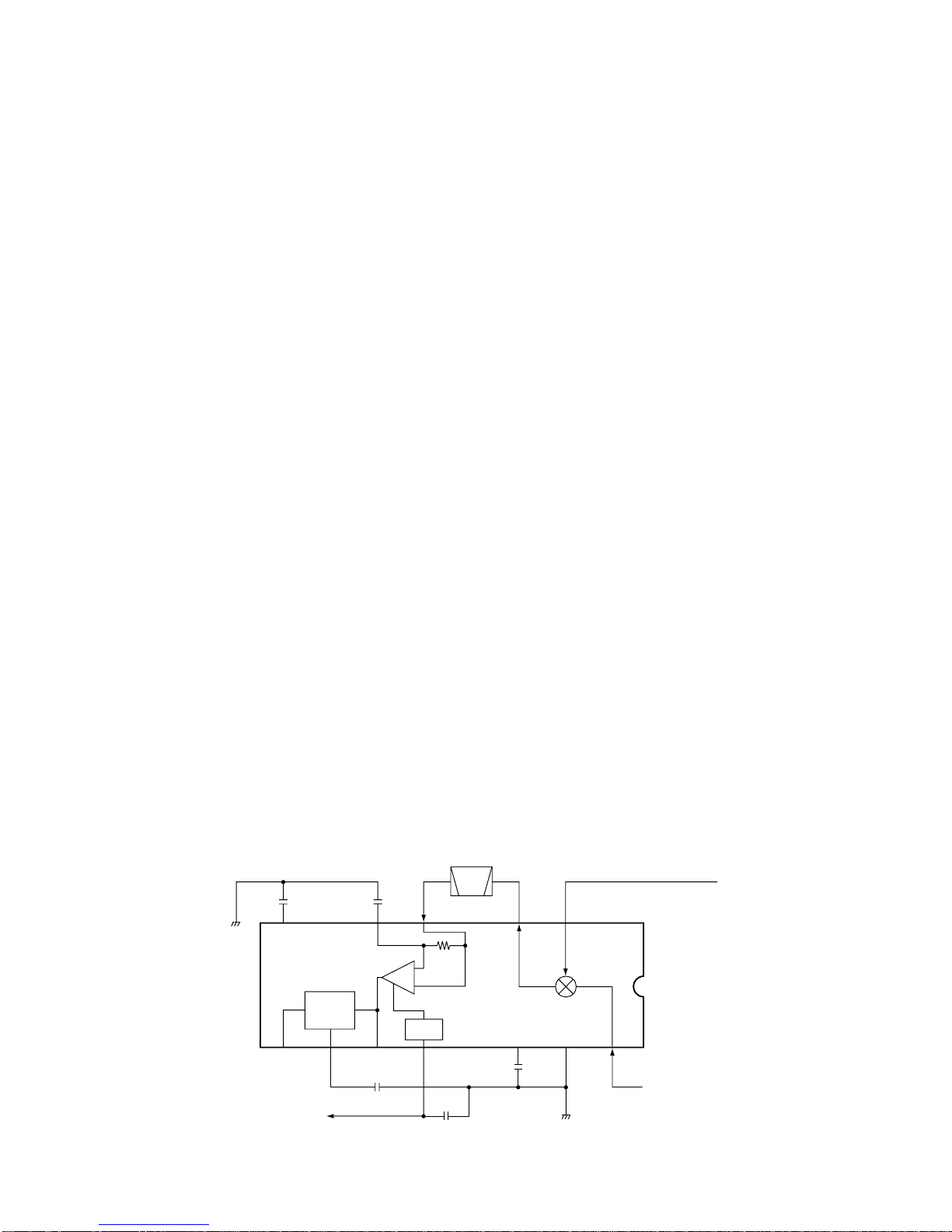
3-5 LOGIC CIRCUITS
3-5-1 CPU AND THE PERIPHERAL CIRCUITS
(LOGIC UNIT)
The LOGIC unit consists of ROM, RAM and 2 kind of CPU
which are 32 bit ARM RISC micro-controller and 8 bit micro-
controller. CPUs and a control circuit control all functions.
The interrupt signal functions in the following way:
•MAIN CPU (IC1)
The main CPU (IC1) is a 32 bit RISC CPU and acts as a
computer circuit to control all functions and to respond to all
kind of interruptions. The main CPU uses a 32 MHz clock sig-
nal from X1.
The main CPU (IC1) generates an address signal and an
RGB signal corresponding to display coordinates and the
address of DRAM. This IC chip also generates vertical sig-
nals and synchronicity signals for the LCD
•SUB CPU (IC22)
The sub CPU controls the LCD brightness, ship speed, key-
board, sounder and serial communication from the GPS,
DGPS, NMEA. The sub CPU uses a RESET signal and 16
MHz clock signal from main CPU (IC1).
•RAM (IC20, IC21)
IC20 is a 4k×9 bit FIFO RAM which buffer strage for sending
received sounder signal from the sub CPU (IC22) to main
CPU (IC1).
IC21 is a 256×8 bit mail-box RAM which communicates GPS
data or keyboard data between the main CPU (IC1) and sub
CPU (IC22).
•ROM (IC32, IC33)
IC32 and IC33 are 8 Mbit flash ROMs. ROM contains a sys-
tem operating program and data of world map.
•ADDRESS DECODER (IC28)
IC28 is a PLD (programmable logic device) which is address
decoder and controller of the card-data reader, and outputs
chip select signal to IC1 and I/O peripheral signals.
•SRAM (IC30, IC31)
IC30 and IC31 are 1 Mbit SRAMs which backuped by the
memory battery (BT1).
•DRAM (IC34, IC35)
IC34, IC35 are DRAMs and are used for video RAMs. Each
chip has a capacity of 4 Mbits.

3 - 4
3-6 DGPS RECEIVER (RD-200)
3-6-1 ANTENNA CIRCUIT (ANT UNIT)
EP3 and EP4 consist of 2 series of antennas respectively
(total 4 series).
The received signal from the antenna (EP3) is tuned at C3,
and is amplified at the RF amplifier circuits (Q1, Q2, Q5, Q6).
On the other hand, the received signal from another antenna
(EP4) which falls at right angle with EP3, is tuned at C4. The
tuned signal is amplified at the RF amplifier circuits (Q3, Q4,
Q7, Q8).
The both amplified signals are piled up and are impedance-
matched to 50 Ωat L1, and are then applied to the MAIN unit
via J1.
3-6-2 RF AMPLIFIER CIRCUIT (MAIN UNIT)
The RF circuit amplifies signals within the range of frequen-
cy coverage and filters out-of-band signals.
The signals from the ANT unit via J1 (pin 2) pass through the
low-pass filter (L2, L3, C3–C7) and high-pass filter (L4,
C8–C10). The filtered signals are amplified at the RF ampli-
fier (IC1) and are then enter another low-pass filter (L6, L7,
C15–C19) and notch filter (L24, L25, C111, C112) to sup-
press unwanted signals. The filtered signals are applied to
the mixer circuit.
3-6-3 MIXER CIRCUIT (MAIN UNIT)
The mixer circuit (IC2, L8, L9) is a double-balanced mixer
which converts the received signal to a fixed frequency of the
IF signal with an LO frequency.
The signals from the RF circuit are mixed with the LO signal
at the mixer circuit (IC2, L8, L9) to produce a 455 kHz IF sig-
nal.
3-6-4 IF CIRCUIT (MAIN UNIT)
By changing the LO frequency, only the desired frequency
will pass through the IF filter at the next stage of the mixer.
The IF signal from the mixer circuit is amplified at the IF
amplifier (Q1) and is applied to a ceramic filter (FI1) to sup-
press out-of-band signals. The filtered signal is applied to the
FM IF IC circuit (IC3).
3-6-5 DEMODULATOR CIRCUIT (MAIN UNIT)
The FM IF IC (IC3) contains the limiter amplifier, detector cir-
cuits, etc.
The IF signal from the IF filter is applied to the limitter ampli-
fier section of IC3 (pin 5). The amplified signal is mixed with
a 456.2 kHz signal from CPU IC (IC12) to produce a 1.2 kHz
detector signal for demodulation the IF signal intoAF signals.
AF signal from FM IF IC (IC3, pin 9) passes through the low-
pass filter (IC4a, IC4b). The filtered signal is amplified at the
AF amplifier (Q4) and is applied to the CPU (IC12).
3-6-6 REFERENCE OSCILLATOR CIRCUIT
(MAIN UNIT)
The reference oscillator circuit generates the reference fre-
quency, and the signals are applied to the DDS IC and CPU.
The generated reference signal from the reference oscillator
(X1: 14.5984 MHz) is amplified and divided at the buffer
amplifier (IC7). The divided signal (7.2992 MHz) is applied to
the DDS IC (IC6) and CPU (IC12) via the amplifiers IC5, IC10
respectively.
3-6-7 LO CIRCUIT (MAIN UNIT)
The LO circuit generates the LO frequency, and the signals
are applied to the mixer circuit.
The generated LO signal is output from IC6 and passed
through the D/A converter (R26–R45), low-pass filter (L15,
L16, C55–C59) and high-pass filter (L17, C60–C62). The fil-
tered signal is amplified at the buffer amplifier (Q2) and then
is passed through the low-pass filter (L18, L19, C65–C69).
The filtered signal is applied to the mixer circuit.
3-7 PORT ALLOCATIONS
3-7-1 FP-561
•SUB CPU (LOGIC UNIT; IC22)
Outputs Tx (50 kHz/200 kHz) pulse sig-
nals to IC1 (pins 1, 3).
Outputs control signal for LCD back-
light.
Outputs control signal for the LCD con-
trast
A/D input port for the received signal
strength indicator voltage.
Input port for serial signal from the
GPS unit via the buffer amplifier (IC23,
pin 12).
Outputs serial signal to the buffer
amplifier (IC23, pin 3) for the GPS unit.
Input port for serial signal from the
NMEA/DGPS units via the analog
switch (IC41, pin 14).
Outputs serial signal to the analog
switch (IC41, pin 2) for the
NMEA/DGPS units.
Ship speed input port from the photo
coupler (IC7, pin 7) on the MAIN unit.
Outputs beep audio to the buzzer cir-
cuit (Q4, SP1) on the SW unit.
Outputs receive frequency switching
signal for the analog switch (IC16).
Outputs trasmit triger signal for the dri-
ver circuit (IC2, pins 2, 6) on the MAIN
unit.
1
3
4
7
16
17
18
20
72
74
77
80
TXSIG
INV
CONT
RSSI
GPSI
GPSO
NMEAI
NMO
SPD
BEEP
LOC
TXTRG
Pin Port Description
number name

FP-561
•MAIN CPU (LOGIC UNIT; IC1)
3-7-2 RD-200
•CPU (MAIN unit; IC12)
3 - 5
Outputs serial clock signal for the LCD.
Outputs vertical synchronizing signal
for LCD.
Outputs horizintal synchronizing signal
for LCD.
Outputs red color signal for LCD.
Outputs blue color signal for LCD.
Outputs green color signal for LCD.
Outputs RX pass-bandwidth control
signal for the RSSI controller (Q25).
High : While narrow
73
86
88
92
93
94
172
DTCK
VSYNC
HSYNC
RED
BLUE
GREEN
DEPCONT
Pin Port Description
number name
Input port for the reset signal from the
reset circuit (IC11, Q5).
8 bit D/Aoutput ports for the bar anten-
nas control signals.
Outputs reset signal for the DDS IC
(IC6).
Outputs serial clock signal for the DDS
IC (IC6).
Outputs serial data signals for the
DDS IC (IC6).
Outputs strobe signals for the DDS IC
(IC6).
Outputs clock signal for the EEPROM
IC (IC13).
Inputs/outputs serial signal for the
EEPROM IC (IC13).
Outputs chip select signal for the EEP-
ROM IC (IC13).
Input port for NMEA signal or clone
signal from the NMEA connector (J3).
Outputs NMEA signal to the NMEA
connector (J3).
10
25–32
39
40
41
42
43
44
45
48
49
RESET
TUNE0–
TUNE7
DRES
CLK
DATA
STRB
ESCK
ESIO
ECS
RXDO
TXDO
Pin Port Description
number name

4 - 1
SECTION 4 ADJUSTMENT PROCEDURES
4-1 PREPARATION
‘‘REQUIRED TEST EQUIPMENT
‘‘CONNECTION
EQUIPMENT
DC power supply
Frequency counter
DC voltmeter
Spectrum analyzer
GRADE AND RANGE
Output voltage : 11–30 V DC
Current capacity : 3 A or more
Frequency range : 0.1–10 MHz
Frequency accuracy: ±1 ppm or better
Sensitivity : 100 mV or better
Input impedance : 50 kΩ/V DC or better
Frequency range : At least 10 MHz
Spectrum bandwidth: ±100 kHz or more
EQUIPMENT
Oscilloscope
Tracking generator
Standard signal
generator (SSG)
GRADE AND RANGE
Frequency range : DC–20 MHz
Measuring range : 0.01–10 V
Frequency range : 100 kHz–100 MHz
Output level : 1 mV to 71 mV
(–47 dBm to –10 dBm)
Frequency range : 10 kHz–100 MHz
Output level : 0.1 µV–32 mV
(–127 to –17 dBm)
TRANSDUCER
FP-561
Marine
Ploter/Sounder
EX-1622
Transom-
type
transducer
(Option)
Coupler
Standard signal
generator
EX-1010
Through-hull type
transducer
(Option)
Coupler R
RDD
FP-561 SSG
D: 1N4002
R: 100 Ω(3 W)
DGPS
RD-200
Differential
GPS receiver
Standard signal
generator
Spectrum
analyzer
Tracking
generator
Frequency
counter
A coupler should be prepared by each
user. The coupler will protect the signal
generator from transmitter power.
RD-200 adjustment
Ground
Battery
11 to 30 VDC Red: + Black: –
PWR
GND

4 - 2
4-2 FP-561 TRANSMITTER ADJUSTMENT
OUTPUT
POWER
ADJUSTMENT
ADJUSTMENT ADJUSTMENT CONDITION MEASUREMENT VALUE POINT
UNIT LOCATION UNIT ADJUST
1
2
•Connect a transducer to the
[TRANSDUCER] connector.
•Mode : [SOUNDER]
•Frequency : [H]
•Depth range : 640 m
•Frequency : [L]
MAIN Connect an oscillo-
scope between pin
3 and pin 5 of J2.
880–1320 Vp-p
at maximum wave
point
Verify
Verify
4-4 FP-561 WATER TEMPERTURE ADJUSTMENT
WATER
TEMPERATURE
ADJUSTMENT
ADJUSTMENT ADJUSTMENT CONDITION MEASUREMENT VALUE POINT
UNIT LOCATION UNIT ADJUST
1•Connect a 10 kΩresistor
between pin 6 and pin 7 of the
[TRANSDUCER] connector J2.
Display 25.0 ˚C LOGIC R131
*This output level of the standard signal generator (SSG) is indicated as SSG’s open circuit.
4-3 FP-561 RECEIVER ADJUSTMENT
RECEIVE
SENSITIVITY
ADJUSTMENT
ADJUSTMENT ADJUSTMENT CONDITION MEASUREMENT VALUE POINT
UNIT LOCATION UNIT ADJUST
1
2
3
•Mode : [SOUNDER]
•Frequency : [H]
•Depth range : 5 m
•STC : [1]
•Connect a standard signal gener-
ator to the [TRANSDUCER] con-
nector J2 via the coupler and set
as:
Fequency : 200 kHz
Level :
1 mV (–47 dBm)
•Frequency : [L]
•Set an SSG as:
Frequency : 50 kHz
Level :
1 mV (–47 dBm)
•Set an SSG as:
Frequency : 50 kHz
Level :
100 mV (–7 dBm)
MAIN Connect a DC volt-
meter or oscillo-
scope to the check
point “RSSI”.
Maximum DC voltage MAIN L1
L6
R99

4 - 3
RSSI
Pin 3
Pin 5
R99
L1
L6
Receive sensitivity
check point
Receive sensitivity
adjustment
Output power
check point J2
Pin 6
Pin 7 Water temperature
pre-setting J2
•MAIN unit
R131
Water temperature
adjustment
•LOGIC unit

4 - 4
*This output level of the standard signal generator (SSG) is indicated as SSG’s open circuit.
4-5 RD-200 ADJUSTMENTS
REFERENCE
FREQUENCY
RECEIVE
SENSITIVITY
DECODE
ANTENNA
(EP3)
(EP4)
ADJUSTMENT
ADJUSTMENT ADJUSTMENT CONDITION MEASUREMENT VALUE POINT
UNIT LOCATION UNIT ADJUST
1
1
1
2
1
2
3
4
•Connect the antenna connector
to the FP-561’s DGPS connector
and turn FP-561 power ON.
•Set the connected FP-561 as:
Baud rate : 200
Fequency : 300.0 kHz
•Connect a standard signal gener-
ator to J4 on the ANT unit and set
as:
Fequency : 300.0 kHz
Modulation : OFF
•Set the connected FP-561 as:
Baud rate : 200
Fequency : 300.0 kHz
•Connect a standard signal gener-
ator to J4 on the ANT unit and set
as:
Fequency : 250.0 kHz
Level :
1 mV (–47 dBm)
Modulation : OFF
•Set an SSG as:
Frequency : 350.0 kHz
•Set the connected FP-561 as:
Baud rate : 200
Fequency : 300.0 kHz
•Remove solder at CP1 on the
ANT unit.
•Conncet a traking generator (or
SSG) to the EP3 on the ANT unit
using the probe JIG and set as:
Level :
7.1 mV (–30 dBm)
Frequency : 300.0 kHz
(SSG only)
•Conncet a TG (or SSG) to the
EP4 on the ANT unit using the
probe Jig and set as:
Level :
7.1 mV (–30 dBm)
Frequency : 300.0 kHz
(SSG only)
MAIN
ANT
MAIN
ANT
Connect a frequen-
cy counter to the
check point “CP1”.
Connect a SINAD
meter to J3.
Connect a DC volt-
meter or oscillo-
scope to the check
point “CP2”.
Connect a spectrum
analyzer to J5.
7.29920 MHz
25 % distortion
High level (5 V)
Low level (0 V)
TG
Peak point to 300 kHz
SSG
Maximum RF level
–40 dBm or more
TG
Peak point to 300 kHz
SSG
Maximum RF level
–40 dBm or more
MAIN
SSG
ANT
C71
Verify the
SSG level
less than
0.2 µV (–
121 dBm)
Verify
Verify
C3
Verify
C4
Verify
After adjustment, re-solder CP1 on the ANT unit.
+–
10.2(d) mm
12.2(d) mm
to TG (SSG) output
ANT unit
EP4
EP3
Kind : enamelled wire
Diameter : 1.0 mm
Roll number : 2 roll
Squeeze to
PC board's edge
Wire description
•Probe JIG

4 - 5
C71
Reference frequency
adjustment
CP2
Decode
check point
CP1
Reference frequency
check point
•MAIN unit
C3
Antenna peak
adjustment for EP3
C4
Antenna peak
adjustment for EP4
J3
Receive sensitivity
check point
CP1
Antenna peak
pre-setting
J5
Antenna peak
check point
J5
RF input
Receive sensitivity
Decode
•ANT unit

5-1 FP-561
[MAIN UNIT]
IC1 1130005720 S.IC TC7W04F (TE12L)
IC2 1130006370 S.IC TC4093BF
IC3 1130007990 S.IC TC3W03FU (TE12L)
IC4 1130007990 S.IC TC3W03FU (TE12L)
IC5 1110003490 S.IC TA31136FN (D,EL)
IC6 1110003340 S.IC µPC358GR-T1
IC7 1130007420 S.IC TC7W14FU (TE12L)
IC8 1170000280 S.IC TLP121 (GB-TPL)
IC9 1110003070 S.IC µPC494GS
IC10 1170000280 S.IC TLP121 (GB-TPL)
IC11 1110002700 S.IC NJM2904M-T1
IC13 1180001840 IC PQ05RF21
IC14 1130003920 S.IC TC4S69F (TE85R)
IC15 1170000280 S.IC TLP121 (GB-TPL)
IC16 1130006220 S.IC TC4W53FU (TE12L)
IC17 1130009480 S.IC TC4049BF (N)
Q1 1530002550 S.TRANSISTOR 2SC3326-B (TE85R)
Q2 1530001950 S.TRANSISTOR 2SC2712-GR (TE85R)
Q3 1530001950 S.TRANSISTOR 2SC2712-GR (TE85R)
Q4 1510000500 S.TRANSISTOR 2SA1162-GR (TE85R)
Q5 1510000500 S.TRANSISTOR 2SA1162-GR (TE85R)
Q6 1590002670 FET FS30KMJ-3
Q7 1590002670 FET FS30KMJ-3
Q12 1510000800 S.TRANSISTOR 2SA1213-Y (TE12R,C)
Q13 1530001950 S.TRANSISTOR 2SC2712-GR (TE85R)
Q14 1590002670 FET FS30KMJ-3
Q16 1510000500 S.TRANSISTOR 2SA1162-GR (TE85R)
Q22 1590000430 S.TRANSISTOR DTC144EUA T106
Q23 1530002550 S.TRANSISTOR 2SC3326-B (TE85R)
Q24 1530002550 S.TRANSISTOR 2SC3326-B (TE85R)
Q25 1530002550 S.TRANSISTOR 2SC3326-B (TE85R)
Q26 1530001950 S.TRANSISTOR 2SC2712-GR (TE85R)
Q27 1540000550 S.TRANSISTOR 2SD1664 T100Q
Q28 1530002060 S.TRANSISTOR 2SC4081 T107 R
Q29 1510000510 S.TRANSISTOR 2SA1576A T106R
Q30 1530002060 S.TRANSISTOR 2SC4081 T107 R
Q31 1510000510 S.TRANSISTOR 2SA1576A T106R
Q32 1530002060 S.TRANSISTOR 2SC4081 T107 R
Q33 1510000510 S.TRANSISTOR 2SA1576A T106R
Q34 1530002060 S.TRANSISTOR 2SC4081 T107 R
Q35 1510000510 S.TRANSISTOR 2SA1576A T106R
D1 1750000550 S.DIODE 1SS355 TE-17
D2 1750000550 S.DIODE 1SS355 TE-17
D3 1710000350 DIODE 1N4002
D4 1710000350 DIODE 1N4002
D9 1710000350 DIODE 1N4002
D10 1790000700 DIODE DSA3A1
D11 1710000350 DIODE 1N4002
D12 1790000760 DIODE RG-2A
D13 1790001630 DIODE SB30-09J
D14 1750000550 S.DIODE 1SS355 TE-17
D17 1710000350 DIODE 1N4002
D18 1730000880 S.ZENER RD11M-T2B2
D21 1750000550 S.DIODE 1SS355 TE-17
D22 1790001630 DIODE SB30-09J
D23 1750000550 S.DIODE 1SS355 TE-17
D24 1750000550 S.DIODE 1SS355 TE-17
D27 1750000130 S.DIODE DA204U T107
D28 1750000550 S.DIODE 1SS355 TE-17
D30 1710000350 DIODE 1N4002
D31 1710000350 DIODE 1N4002
D32 1710000350 DIODE 1N4002
D33 1730000010 S.ZENER RD4.7M-T2B3
D34 1730000010 S.ZENER RD4.7M-T2B3
D35 1710000350 DIODE 1N4002
D36 1710000350 DIODE 1N4002
D37 1730000770 S.ZENER RD7.5M-T1B1
FI1 2020001640 CERAMIC CFWS455GY
X1 6050009190 XTAL CR-497 (5.24 MHz)
X2 6050009180 XTAL CR-496 (4.04 MHz)
L1 6150003680 COIL LS-415
L2 5920000450 COIL FK-080E-1020
L3 6200009060 S.COIL LQH 3C 101K 34
L5 6170000150 COIL LW-16
L6 6150003670 COIL LS-414
L7 6200003240 S.COIL NL 322522T-221J
L8 6200008670 S.COIL D10F-A814AY-152K
R2 7030003560 S.RESISTOR ERJ3GEYJ 103 V (10 kΩ)
R3 7030003560 S.RESISTOR ERJ3GEYJ 103 V (10 kΩ)
R5 7070001040 RESISTOR ERG1SJ 472 (4.7 kΩ)
R6 7070001040 RESISTOR ERG1SJ 472 (4.7 kΩ)
R7 7070000641 RESISTOR ERG2SJ 471 (470 Ω)
R8 7030003280 S.RESISTOR ERJ3GEYJ 470 V (47 Ω)
R9 7030003630 S.RESISTOR ERJ3GEYJ 393 V (39 kΩ)
R10 7030003580 S.RESISTOR ERJ3GEYJ 153 V (15 kΩ)
R12 7030003800 S.RESISTOR ERJ3GEYJ 105 V (1 MΩ)
R13 7030003800 S.RESISTOR ERJ3GEYJ 105 V (1 MΩ)
R15 7030003280 S.RESISTOR ERJ3GEYJ 470 V (47 Ω)
R16 7030003440 S.RESISTOR ERJ3GEYJ 102 V (1 kΩ)
R17 7030003640 S.RESISTOR ERJ3GEYJ 473 V (47 kΩ)
R18 7030003640 S.RESISTOR ERJ3GEYJ 473 V (47 kΩ)
R19 7030003720 S.RESISTOR ERJ3GEYJ 224 V (220 kΩ)
R22 7030003440 S.RESISTOR ERJ3GEYJ 102 V (1 kΩ)
R23 7030003440 S.RESISTOR ERJ3GEYJ 102 V (1 kΩ)
R24 7030003320 S.RESISTOR ERJ3GEYJ 101 V (100 Ω)
R25 7030003320 S.RESISTOR ERJ3GEYJ 101 V (100 Ω)
R26 7030003440 S.RESISTOR ERJ3GEYJ 102 V (1 kΩ)
R27 7030003440 S.RESISTOR ERJ3GEYJ 102 V (1 kΩ)
R28 7030000190 S.RESISTOR MCR10EZHJ 27 Ω(270)
R29 7030000190 S.RESISTOR MCR10EZHJ 27 Ω(270)
R35 7030000340 S.RESISTOR MCR10EZHJ 470 Ω(471)
R36 7030003560 S.RESISTOR ERJ3GEYJ 103 V (10 kΩ)
R44 7030006520 S.RESISTOR RR0816P-561-D (560 Ω)
R45 7030003320 S.RESISTOR ERJ3GEYJ 101 V (100 Ω)
R46 7540000060 ABSORBER ERZ-C05DK 560
R47 7030000470 S.RESISTOR MCR10EZHJ 5.6 kΩ
R48 7030001430 S.RESISTOR MCR50JZHJ 27 kΩ
R55 7030003400 S.RESISTOR ERJ3GEYJ 471 V (470 Ω)
R56 7030003440 S.RESISTOR ERJ3GEYJ 102 V (1 kΩ)
R60 7030000980 S.RESISTOR MCR50JZHJ 5.6 Ω(5R6)
R61 7030000310 S.RESISTOR MCR10EZHJ 270 Ω(271)
R62 7030003480 S.RESISTOR ERJ3GEYJ 222 V (2.2 kΩ)
R63 7030003520 S.RESISTOR ERJ3GEYJ 472 V (4.7 kΩ)
R64 7030003580 S.RESISTOR ERJ3GEYJ 153 V (15 kΩ)
R65 7030003560 S.RESISTOR ERJ3GEYJ 103 V (10 kΩ)
R66 7030000500 S.RESISTOR MCR10EZHJ 10 kΩ
R67 7030003620 S.RESISTOR ERJ3GEYJ 333 V (33 kΩ)
R68 7030003600 S.RESISTOR ERJ3GEYJ 223 V (22 kΩ)
R69 7030003530 S.RESISTOR ERJ3GEYJ 562 V (5.6 kΩ)
R70 7030003530 S.RESISTOR ERJ3GEYJ 562 V (5.6 kΩ)
R71 7030003600 S.RESISTOR ERJ3GEYJ 223 V (22 kΩ)
R72 7030003530 S.RESISTOR ERJ3GEYJ 562 V (5.6 kΩ)
R74 7030003560 S.RESISTOR ERJ3GEYJ 103 V (10 kΩ)
R75 7030003500 S.RESISTOR ERJ3GEYJ 332 V (3.3 kΩ)
R76 7030003560 S.RESISTOR ERJ3GEYJ 103 V (10 kΩ)
R77 7030003600 S.RESISTOR ERJ3GEYJ 223 V (22 kΩ)
R78 7030000410 S.RESISTOR MCR10EZHJ 1.8 kΩ
R79 7030000170 S.RESISTOR MCR10EZHJ 18 Ω(180)
R82 7030003460 S.RESISTOR ERJ3GEYJ 152 V (1.5 kΩ)
R84 7030003560 S.RESISTOR ERJ3GEYJ 103 V (10 kΩ)
R85 7070000641 RESISTOR ERG2SJ 471 (470 Ω)
R91 7030003440 S.RESISTOR ERJ3GEYJ 102 V (1 kΩ)
R92 7030003400 S.RESISTOR ERJ3GEYJ 471 V (470 Ω)
R93 7030003440 S.RESISTOR ERJ3GEYJ 102 V (1 kΩ)
R94 7030003560 S.RESISTOR ERJ3GEYJ 103 V (10 kΩ)
R96 7030003680 S.RESISTOR ERJ3GEYJ 104 V (100 kΩ)
R97 7030003650 S.RESISTOR ERJ3GEYJ 563 V (56 kΩ)
R98 7030003600 S.RESISTOR ERJ3GEYJ 223 V (22 kΩ)
S.=Surface mount
5 - 1
SECTION 5 PARTS LIST
REF ORDER DESCRIPTION
NO. NO. REF ORDER DESCRIPTION
NO. NO.
[MAIN UNIT]

C80 4510004560 ELECTROLYTIC 50 MV 10 NPDW
C81 4030011600 S.CERAMIC C1608 JB 1C 104KT-N
C83 4030006860 S.CERAMIC C1608 JB 1H 102K-T-A
C85 4030006880 S.CERAMIC C1608 JB 1H 472K-T-A
C86 4510004910 ELECTROLYTIC 16 MV 10 SWN
C88 4030011600 S.CERAMIC C1608 JB 1C 104KT-N
C89 4030006860 S.CERAMIC C1608 JB 1H 102K-T-A
C90 4030006900 S.CERAMIC C1608 JB 1E 103K-T-A
C91 4010008470 CERAMIC DE0905 B 222K 1KV
C92 4010008470 CERAMIC DE0905 B 222K 1KV
C93 4030010240 S.CERAMIC C1608 JB 1H 391K-T-A
C94 4010008470 CERAMIC DE0905 B 222K 1KV
C95 4010008470 CERAMIC DE0905 B 222K 1KV
C96 4030008470 S.CERAMIC C1608 JB 1H 272K-T-A
C97 4030011600 S.CERAMIC C1608 JB 1C 104KT-N
C98 4030011600 S.CERAMIC C1608 JB 1C 104KT-N
C99 4030011600 S.CERAMIC C1608 JB 1C 104KT-N
C100 4030011600 S.CERAMIC C1608 JB 1C 104KT-N
C101 4030011600 S.CERAMIC C1608 JB 1C 104KT-N
C102 4550003080 S.TANTALUM TEMSVA 1A 335M-8L
C103 4510004630 S.ELECTROLYTIC ECEV1CA100SR
C104 4030006860 S.CERAMIC C1608 JB 1H 102K-T-A
C105 4030011600 S.CERAMIC C1608 JB 1C 104KT-N
C106 4030011600 S.CERAMIC C1608 JB 1C 104KT-N
C107 4030011600 S.CERAMIC C1608 JB 1C 104KT-N
C108 4030011600 S.CERAMIC C1608 JB 1C 104KT-N
C109 4030011600 S.CERAMIC C1608 JB 1C 104KT-N
C110 4550006250 S.TANTALUM TEMSVA 1A 106M-8L
C111 4030006480 S.CERAMIC GRM42-6 B 104K 50PT
C113 4030006480 S.CERAMIC GRM42-6 B 104K 50PT
C115 4030007040 S.CERAMIC C1608 CH 1H 180J-T-A
C116 4030011280 S.CERAMIC C1608 CH 1H 271J-T-A
C117 4030011280 S.CERAMIC C1608 CH 1H 271J-T-A
C118 4030011600 S.CERAMIC C1608 JB 1C 104KT-N
C119 4030007070 S.CERAMIC C1608 CH 1H 330J-T-A
C120 4030007070 S.CERAMIC C1608 CH 1H 330J-T-A
C121 4030011330 S.CERAMIC C1608 CH 1H 391J-T-A
C122 4030011330 S.CERAMIC C1608 CH 1H 391J-T-A
J1 6510021040 CONNECTOR 52806-3010
J2 6510021220 CONNECTOR 8S-S-E-SS
J3 6510021190 CONNECTOR 2S-S-E-SS
J4 6510021200 CONNECTOR 4S-S-E-SS
J5 6510021210 CONNECTOR 7S-S-E-SS
F1 5210000060 FUSE FGB 5A
F2 5220000020 HOLDER S-N5051
F3 5220000020 HOLDER S-N5051
T1 5920000730 TRANSFORMER TO-46
T2 5920000690 TRANSFORMER TO-43
EP1 0910051392 PCB B 5305B
EP2 0850000120 UNIT BOARD IA023-5B03S
[MAIN UNIT]
R99 7310003580 S.TRIMMER EVM-1XSX50 B15 (104)
R100 7030003400 S.RESISTOR ERJ3GEYJ 471 V (470 Ω)
R101 7030003600 S.RESISTOR ERJ3GEYJ 223 V (22 kΩ)
R102 7030003600 S.RESISTOR ERJ3GEYJ 223 V (22 kΩ)
R103 7030003680 S.RESISTOR ERJ3GEYJ 104 V (100 kΩ)
R104 7030003680 S.RESISTOR ERJ3GEYJ 104 V (100 kΩ)
R105 7030003390 S.RESISTOR ERJ3GEYJ 391 V (390 Ω)
R106 7030003390 S.RESISTOR ERJ3GEYJ 391 V (390 Ω)
R107 7070000641 RESISTOR ERG2SJ 471 (470 Ω)
R108 7030003600 S.RESISTOR ERJ3GEYJ 223 V (22 kΩ)
R109 7030003680 S.RESISTOR ERJ3GEYJ 104 V (100 kΩ)
R110 7030003680 S.RESISTOR ERJ3GEYJ 104 V (100 kΩ)
R111 7030003680 S.RESISTOR ERJ3GEYJ 104 V (100 kΩ)
R112 7030003680 S.RESISTOR ERJ3GEYJ 104 V (100 kΩ)
R113 7030003680 S.RESISTOR ERJ3GEYJ 104 V (100 kΩ)
R115 7030003370 S.RESISTOR ERJ3GEYJ 271 V (270 Ω)
R116 7030003540 S.RESISTOR ERJ3GEYJ 682 V (6.8 kΩ)
R117 7030003440 S.RESISTOR ERJ3GEYJ 102 V (1 kΩ)
R118 7030003480 S.RESISTOR ERJ3GEYJ 222 V (2.2 kΩ)
R119 7030003440 S.RESISTOR ERJ3GEYJ 102 V (1 kΩ)
R120 7030003440 S.RESISTOR ERJ3GEYJ 102 V (1 kΩ)
R122 7030001090 S.RESISTOR MCR50JZHJ 47 Ω(470)
R124 7030001090 S.RESISTOR MCR50JZHJ 47 Ω(470)
R125 7030003440 S.RESISTOR ERJ3GEYJ 102 V (1 kΩ)
R127 7030001090 S.RESISTOR MCR50JZHJ 47 Ω(470)
R128 7030003440 S.RESISTOR ERJ3GEYJ 102 V (1 kΩ)
R130 7030001090 S.RESISTOR MCR50JZHJ 47 Ω(470)
R131 7030003280 S.RESISTOR ERJ3GEYJ 470 V (47 Ω)
C1 4030011600 S.CERAMIC C1608 JB 1C 104KT-N
C3 4030007130 S.CERAMIC C1608 CH 1H 101J-T-A
C4 4030007130 S.CERAMIC C1608 CH 1H 101J-T-A
C5 4030011600 S.CERAMIC C1608 JB 1C 104KT-N
C7 4030006860 S.CERAMIC C1608 JB 1H 102K-T-A
C8 4510004630 S.ELECTROLYTIC ECEV1CA100SR
C10 4030011600 S.CERAMIC C1608 JB 1C 104KT-N
C11 4030009990 S.CERAMIC C1608 CH 1H 200J-T-A
C12 4030009990 S.CERAMIC C1608 CH 1H 200J-T-A
C13 4030009990 S.CERAMIC C1608 CH 1H 200J-T-A
C14 4030009990 S.CERAMIC C1608 CH 1H 200J-T-A
C16 4030011600 S.CERAMIC C1608 JB 1C 104KT-N
C17 4550006250 S.TANTALUM TEMSVA 1A 106M-8L
C18 4030006860 S.CERAMIC C1608 JB 1H 102K-T-A
C19 4030006900 S.CERAMIC C1608 JB 1E 103K-T-A
C20 4030006860 S.CERAMIC C1608 JB 1H 102K-T-A
C21 4030006900 S.CERAMIC C1608 JB 1E 103K-T-A
C22 4030006900 S.CERAMIC C1608 JB 1E 103K-T-A
C23 4030006900 S.CERAMIC C1608 JB 1E 103K-T-A
C24 4030011600 S.CERAMIC C1608 JB 1C 104KT-N
C25 4030011600 S.CERAMIC C1608 JB 1C 104KT-N
C28 4510007030 ELECTROLYTIC 63 MV 1000CZ
C40 4510005310 S.ELECTROLYTIC ECEV1CA220SR
C41 4030006900 S.CERAMIC C1608 JB 1E 103K-T-A
C42 4030006860 S.CERAMIC C1608 JB 1H 102K-T-A
C43 4030006900 S.CERAMIC C1608 JB 1E 103K-T-A
C44 4510007020 ELECTROLYTIC 35 MV 1000GX
C45 4030004740 S.CERAMIC C2012 JB 1H 472K-T-A
C46 4030004740 S.CERAMIC C2012 JB 1H 472K-T-A
C47 4510007020 ELECTROLYTIC 35 MV 1000GX
C48 4030004740 S.CERAMIC C2012 JB 1H 472K-T-A
C49 4030004740 S.CERAMIC C2012 JB 1H 472K-T-A
C50 4310000360 MYLAR 50 F2D 103J
C52 4510006880 ELECTROLYTIC 100 MV 33 CZ
C53 4510007010 ELECTROLYTIC 16 MV 1000GX
C54 4510006640 ELECTROLYTIC 16 MV 1000 CZ
C59 4510004940 ELECTROLYTIC 50 MV 33 NPDW
C60 4510004940 ELECTROLYTIC 50 MV 33 NPDW
C61 4030006880 S.CERAMIC C1608 JB 1H 472K-T-A
C62 4030011600 S.CERAMIC C1608 JB 1C 104KT-N
C63 4510004640 S.ELECTROLYTIC ECEV1CA470SP
C64 4030008920 S.CERAMIC C1608 JB 1C 473K-T-A
C69 4510007000 ELECTROLYTIC 10 MV 1000GX
C70 4030006900 S.CERAMIC C1608 JB 1E 103K-T-A
C71 4030006900 S.CERAMIC C1608 JB 1E 103K-T-A
C72 4510005940 ELECTROLYTIC 10 MV 470 HC
C73 4030006900 S.CERAMIC C1608 JB 1E 103K-T-A
C74 4030006900 S.CERAMIC C1608 JB 1E 103K-T-A
C75 4510005750 S.ELECTROLYTIC ECEV1EA220SP
C76 4510004640 S.ELECTROLYTIC ECEV1CA470SP
C77 4310000570 MYLAR 50 F2D 222J
C79 4510004640 S.ELECTROLYTIC ECEV1CA470SP
5 - 2
S.=Surface mount
REF ORDER DESCRIPTION
NO. NO.
[MAIN UNIT]
REF ORDER DESCRIPTION
NO. NO.

REF ORDER DESCRIPTION
NO. NO.
R46 7030003260 S.RESISTOR ERJ3GEYJ 330 V (33 Ω)
R47 7030003580 S.RESISTOR ERJ3GEYJ 153 V (15 kΩ)
R48 7030003580 S.RESISTOR ERJ3GEYJ 153 V (15 kΩ)
R49 7030003580 S.RESISTOR ERJ3GEYJ 153 V (15 kΩ)
R51 7030003260 S.RESISTOR ERJ3GEYJ 330 V (33 Ω)
R52 7030003260 S.RESISTOR ERJ3GEYJ 330 V (33 Ω)
R53 7030003260 S.RESISTOR ERJ3GEYJ 330 V (33 Ω)
R55 7030003520 S.RESISTOR ERJ3GEYJ 472 V (4.7 kΩ)
R56 7030003580 S.RESISTOR ERJ3GEYJ 153 V (15 kΩ)
R60 7030003580 S.RESISTOR ERJ3GEYJ 153 V (15 kΩ)
R62 7030003600 S.RESISTOR ERJ3GEYJ 223 V (22 kΩ)
R68 7030003800 S.RESISTOR ERJ3GEYJ 105 V (1 MΩ)
R71 7030003580 S.RESISTOR ERJ3GEYJ 153 V (15 kΩ)
R77 7030003260 S.RESISTOR ERJ3GEYJ 330 V (33 Ω)
R78 7030003580 S.RESISTOR ERJ3GEYJ 153 V (15 kΩ)
R81 7030003580 S.RESISTOR ERJ3GEYJ 153 V (15 kΩ)
R82 7030003580 S.RESISTOR ERJ3GEYJ 153 V (15 kΩ)
R83 7030003580 S.RESISTOR ERJ3GEYJ 153 V (15 kΩ)
R85 7030003640 S.RESISTOR ERJ3GEYJ 473 V (47 kΩ)
R86 7030003640 S.RESISTOR ERJ3GEYJ 473 V (47 kΩ)
R87 7030003640 S.RESISTOR ERJ3GEYJ 473 V (47 kΩ)
R88 7030003640 S.RESISTOR ERJ3GEYJ 473 V (47 kΩ)
R89 7030003640 S.RESISTOR ERJ3GEYJ 473 V (47 kΩ)
R90 7030003580 S.RESISTOR ERJ3GEYJ 153 V (15 kΩ)
R91 7030003580 S.RESISTOR ERJ3GEYJ 153 V (15 kΩ)
R92 7030003580 S.RESISTOR ERJ3GEYJ 153 V (15 kΩ)
R93 7030003580 S.RESISTOR ERJ3GEYJ 153 V (15 kΩ)
R94 7030003580 S.RESISTOR ERJ3GEYJ 153 V (15 kΩ)
R95 7030003580 S.RESISTOR ERJ3GEYJ 153 V (15 kΩ)
R96 7030003580 S.RESISTOR ERJ3GEYJ 153 V (15 kΩ)
R97 7030003580 S.RESISTOR ERJ3GEYJ 153 V (15 kΩ)
R98 7030003580 S.RESISTOR ERJ3GEYJ 153 V (15 kΩ)
R99 7030003580 S.RESISTOR ERJ3GEYJ 153 V (15 kΩ)
R100 7030003580 S.RESISTOR ERJ3GEYJ 153 V (15 kΩ)
R101 7030003580 S.RESISTOR ERJ3GEYJ 153 V (15 kΩ)
R102 7030003580 S.RESISTOR ERJ3GEYJ 153 V (15 kΩ)
R104 7030003640 S.RESISTOR ERJ3GEYJ 473 V (47 kΩ)
R105 7030003640 S.RESISTOR ERJ3GEYJ 473 V (47 kΩ)
R106 7030003580 S.RESISTOR ERJ3GEYJ 153 V (15 kΩ)
R107 7030003580 S.RESISTOR ERJ3GEYJ 153 V (15 kΩ)
R108 7030003580 S.RESISTOR ERJ3GEYJ 153 V (15 kΩ)
R109 7030003580 S.RESISTOR ERJ3GEYJ 153 V (15 kΩ)
R110 7030003580 S.RESISTOR ERJ3GEYJ 153 V (15 kΩ)
R111 7030003580 S.RESISTOR ERJ3GEYJ 153 V (15 kΩ)
R112 7030003580 S.RESISTOR ERJ3GEYJ 153 V (15 kΩ)
R126 7030003580 S.RESISTOR ERJ3GEYJ 153 V (15 kΩ)
R127 7030003580 S.RESISTOR ERJ3GEYJ 153 V (15 kΩ)
R128 7030003580 S.RESISTOR ERJ3GEYJ 153 V (15 kΩ)
R129 7030003580 S.RESISTOR ERJ3GEYJ 153 V (15 kΩ)
R130 7030003580 S.RESISTOR ERJ3GEYJ 153 V (15 kΩ)
R131 7310003610 S.TRIMMER EVM-1XSX50 B14 (103)
R132 7030003260 S.RESISTOR ERJ3GEYJ 330 V (33 Ω)
R133 7030003580 S.RESISTOR ERJ3GEYJ 153 V (15 kΩ)
R134 7030003680 S.RESISTOR ERJ3GEYJ 104 V (100 kΩ)
R135 7030003680 S.RESISTOR ERJ3GEYJ 104 V (100 kΩ)
R136 7030003580 S.RESISTOR ERJ3GEYJ 153 V (15 kΩ)
R138 7030003640 S.RESISTOR ERJ3GEYJ 473 V (47 kΩ)
R140 7030003520 S.RESISTOR ERJ3GEYJ 472 V (4.7 kΩ)
R142 7030003580 S.RESISTOR ERJ3GEYJ 153 V (15 kΩ)
R143 7030003260 S.RESISTOR ERJ3GEYJ 330 V (33 Ω)
R144 7030003320 S.RESISTOR ERJ3GEYJ 101 V (100 Ω)
R145 7030003320 S.RESISTOR ERJ3GEYJ 101 V (100 Ω)
R146 7030003320 S.RESISTOR ERJ3GEYJ 101 V (100 Ω)
R147 7030003440 S.RESISTOR ERJ3GEYJ 102 V (1 kΩ)
R148 7030003580 S.RESISTOR ERJ3GEYJ 153 V (15 kΩ)
R150 7030003580 S.RESISTOR ERJ3GEYJ 153 V (15 kΩ)
R151 7030003220 S.RESISTOR ERJ3GEYJ 150 V (15 Ω)
R155 7030006600 S.RESISTOR RR0816P-822-D (8.2 kΩ)
R156 7030003320 S.RESISTOR ERJ3GEYJ 101 V (100 Ω)
R162 7030003580 S.RESISTOR ERJ3GEYJ 153 V (15 kΩ)
R163 7030003440 S.RESISTOR ERJ3GEYJ 102 V (1 kΩ)
R164 7030003360 S.RESISTOR ERJ3GEYJ 221 V (220 Ω)
R165 7030003320 S.RESISTOR ERJ3GEYJ 101 V (100 Ω)
R167 7030003560 S.RESISTOR ERJ3GEYJ 103 V (10 kΩ)
R168 7030003560 S.RESISTOR ERJ3GEYJ 103 V (10 kΩ)
R169 7030003560 S.RESISTOR ERJ3GEYJ 103 V (10 kΩ)
R170 7030003560 S.RESISTOR ERJ3GEYJ 103 V (10 kΩ)
R171 7030003560 S.RESISTOR ERJ3GEYJ 103 V (10 kΩ)
R172 7030003560 S.RESISTOR ERJ3GEYJ 103 V (10 kΩ)
R173 7030003560 S.RESISTOR ERJ3GEYJ 103 V (10 kΩ)
R174 7030003560 S.RESISTOR ERJ3GEYJ 103 V (10 kΩ)
R177 7030003500 S.RESISTOR ERJ3GEYJ 332 V (3.3 kΩ)
S.=Surface mount
IC1 1140007500 S.IC CL-PS7500FE-QC-A
IC2 1130009170 S.IC TC74HCT245AF
IC3 1130009170 S.IC TC74HCT245AF
IC4 1130005440 S.IC TC74HC245AF
IC5 1130005440 S.IC TC74HC245AF
IC6 1130005440 S.IC TC74HC245AF
IC7 1130009390 IC TC74HCT646AP
IC13 1110003500 S.IC S-80742SL-A6-T1
IC16 1130005340 S.IC TC74HC139AF
IC18 1130005480 S.IC TC74HC573AF
IC19 1130007040 S.IC TC7W32F (TE12L)
IC20 1130009080 S.IC CY7C433-40JC
IC21 1140007540 S.IC M66220FP
IC22 1140007510 S.IC TMP90PM36F
IC23 1130005290 S.IC TC74HC14AF
IC28 1140007820 S.IC SC-1372 (MACH111-15JC)
IC30 1130009050 S.IC M5M51008BVP-70LL
IC31 1130009050 S.IC M5M51008BVP-70LL
IC32 1130009060 S.IC MBM29F800BA-90PFTN
IC33 1130009060 S.IC MBM29F800BA-90PFTN
IC34 1140007570 S.IC M5M44260CJ
IC35 1140007570 S.IC M5M44260CJ
IC41 1130007680 S.IC BU4053BCF-T1
IC42 1130005290 S.IC TC74HC14AF
IC44 1130008040 S.IC TC7SH04FU
IC45 1130005741 S.IC TC74AC74F (TP1)
IC46 1130008040 S.IC TC7SH04FU
Q1 1530001950 S.TRANSISTOR 2SC2712-GR (TE85R)
Q3 1520000450 S.TRANSISTOR 2SB1132 T100 Q
Q4 1520000650 S.TRANSISTOR 2SB1201-S-TL
Q5 1590001190 S.TRANSISTOR XP6501-(TX) .AB
D1 1750000060 S.DIODE 1SS196 (TE85R)
D2 1750000020 S.DIODE 1SS184 (TE85R)
X1 6050010460 S.XTAL DSO-49SJ (32.000 MHz)
R1 7030003640 S.RESISTOR ERJ3GEYJ 473 V (47 kΩ)
R2 7030003680 S.RESISTOR ERJ3GEYJ 104 V (100 kΩ)
R3 7030003760 S.RESISTOR ERJ3GEYJ 474 V (470 kΩ)
R4 7030003720 S.RESISTOR ERJ3GEYJ 224 V (220 kΩ)
R5 7030003580 S.RESISTOR ERJ3GEYJ 153 V (15 kΩ)
R6 7030003580 S.RESISTOR ERJ3GEYJ 153 V (15 kΩ)
R7 7030003580 S.RESISTOR ERJ3GEYJ 153 V (15 kΩ)
R8 7030003580 S.RESISTOR ERJ3GEYJ 153 V (15 kΩ)
R9 7030003580 S.RESISTOR ERJ3GEYJ 153 V (15 kΩ)
R10 7030003580 S.RESISTOR ERJ3GEYJ 153 V (15 kΩ)
R11 7030003580 S.RESISTOR ERJ3GEYJ 153 V (15 kΩ)
R12 7030003580 S.RESISTOR ERJ3GEYJ 153 V (15 kΩ)
R13 7030003580 S.RESISTOR ERJ3GEYJ 153 V (15 kΩ)
R14 7030003580 S.RESISTOR ERJ3GEYJ 153 V (15 kΩ)
R15 7030003580 S.RESISTOR ERJ3GEYJ 153 V (15 kΩ)
R16 7030003580 S.RESISTOR ERJ3GEYJ 153 V (15 kΩ)
R17 7030003580 S.RESISTOR ERJ3GEYJ 153 V (15 kΩ)
R18 7030003580 S.RESISTOR ERJ3GEYJ 153 V (15 kΩ)
R19 7030003580 S.RESISTOR ERJ3GEYJ 153 V (15 kΩ)
R20 7030003580 S.RESISTOR ERJ3GEYJ 153 V (15 kΩ)
R21 7030003640 S.RESISTOR ERJ3GEYJ 473 V (47 kΩ)
R22 7030003640 S.RESISTOR ERJ3GEYJ 473 V (47 kΩ)
R23 7030003640 S.RESISTOR ERJ3GEYJ 473 V (47 kΩ)
R24 7030003640 S.RESISTOR ERJ3GEYJ 473 V (47 kΩ)
R25 7030003640 S.RESISTOR ERJ3GEYJ 473 V (47 kΩ)
R26 7030003640 S.RESISTOR ERJ3GEYJ 473 V (47 kΩ)
R27 7030003640 S.RESISTOR ERJ3GEYJ 473 V (47 kΩ)
R28 7030003640 S.RESISTOR ERJ3GEYJ 473 V (47 kΩ)
R29 7030003640 S.RESISTOR ERJ3GEYJ 473 V (47 kΩ)
R30 7030003640 S.RESISTOR ERJ3GEYJ 473 V (47 kΩ)
R31 7030003640 S.RESISTOR ERJ3GEYJ 473 V (47 kΩ)
R32 7030003560 S.RESISTOR ERJ3GEYJ 103 V (10 kΩ)
R36 7030003560 S.RESISTOR ERJ3GEYJ 103 V (10 kΩ)
R37 7030003580 S.RESISTOR ERJ3GEYJ 153 V (15 kΩ)
R38 7030003580 S.RESISTOR ERJ3GEYJ 153 V (15 kΩ)
R39 7030003580 S.RESISTOR ERJ3GEYJ 153 V (15 kΩ)
R40 7030003580 S.RESISTOR ERJ3GEYJ 153 V (15 kΩ)
R41 7030003580 S.RESISTOR ERJ3GEYJ 153 V (15 kΩ)
R42 7030003480 S.RESISTOR ERJ3GEYJ 222 V (2.2 kΩ)
R43 7030003580 S.RESISTOR ERJ3GEYJ 153 V (15 kΩ)
R44 7030003560 S.RESISTOR ERJ3GEYJ 103 V (10 kΩ)
R45 7030003260 S.RESISTOR ERJ3GEYJ 330 V (33 Ω)
5 - 3
REF ORDER DESCRIPTION
NO. NO.
[LOGIC UNIT] [LOGIC UNIT]
Other manuals for FP-561
2
This manual suits for next models
1
Table of contents
Other Icom Marine Equipment manuals
Popular Marine Equipment manuals by other brands

Alamarin Jet
Alamarin Jet AJ 285 Repair manual

Facnor
Facnor FD110 installation manual

Jeppesen
Jeppesen Nobeltec SSHS owner's manual

Lewmar
Lewmar V1 Owners installation, operation & basic servicing manual

Texecom
Texecom Premier Elite Odyssey 5-W quick start guide

Vetus
Vetus TMWQ Installation instructions and operation manual

E2S
E2S A100SONTEL Instructions/service manual

Vixen Horns
Vixen Horns VXS-9080SCL installation guide

Raymarine
Raymarine i50 Depth Installation and operation instructions

JRC
JRC Alphatron Marine Mode Switch 3 Pos Operation manual

Webasto
Webasto BlueCool S Series installation instructions

E2S
E2S STExC1 instruction manual