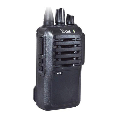
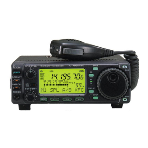
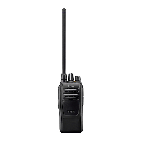
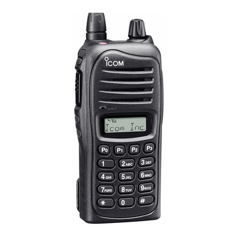
Icom IC-F1010 User manual

lc-Frolo
lc-Flo2()
lcom
Inc.
VHFPRIVATEMOBILERADIO
lc-Frolo
VHFLANDMOBILERADIO

.:,G
INTRODUCTION
Thisservice
manual
describesthe
latestserviceinformationfor
thelGFl010
VHFPRIVATEMOBILERADIOandlC-Fl020
VHFLAND
MOBILERADIOatthetimeof
publication.
To
upgrade
quality,
anyelectricalor
mechanical
parts
and
internalcircuitsaresubjecttochange
withoutnotice
or
obligation.
ORDERING
PARTS
Besuretoincludethefollowingfour
points
whenordering
rep!acementparts:
1
.lGdigitorder
numbers
2.
Component
pad
number
andname
3.Equipmentmodelname
andunitname
4.
Quantity
required
dAMPLEORDER>
1110003570
S.lC MC3372 lC-F1010MAINUNIT 5
pieces
8810008660ScrewBTM3x8NI-ZUlGF1010Bottomcover10
oieces
Addresses
are
orovidedonthe
inside
backcover
for
vour
convenience.
DANGER
NEVER
connect
thetransceiver
toan
AC
outletortoa DC
power
supply
thatusesmore
than16
V. Thiswillruin
the
itransceiver.
DONOT
exposethe
transceiver
torain,
snoworany
liquids.
DONOTreverse
the
polarities
ofthe
power
supplywhen
connecting
thetransceiver.
DONOT
apply
anRFsignal
ofmorethan20
dBm
(100
mW)
to
theantenna
connector.
Thiscould
damagethe
transceiver's
front
end.
I
REPAIR
NOTES
Make
sure
aproblem
isinternal
before
disassemblingthe
transceiver.
DONOT
open
thetransceiver
until
thetransceiveris
disconnected
from
its
power
source.
DONOT
force
anyof
the
variable
components.Turn
them
slowly
andsmoothly.
'
DO
NOT
shorlany
circuitsor
electronic
parts.
Aninsulated
tuning
toolMUST
be
used
for
alladjustments.
DONOT
keep
power
ONfor
a long
timewhen
the
transceiveris
defective.
DONOT
transmit
power
into
asignal
generator
or
asweep
generator.
ALWAYS
connect
a40
dBto50dBattenuatorbetween
the
transceiver
and
a deviationmeter
orspectrum
analyzerwhen
using
suchtest
equipment.
READ
theinstructions
oftest
equipmentthoroughly
before
connecting
equipment
tothetransceiver.
a
5.
7.

)c
he EXPLICIT
DEFINITIONS
b.
en
to
t's
Model Version
number Frequency
covelage Channel
spacing Power
rc-F1010
tPMRl
#o1 L-band,
136-155
MHz 12.5 kHz 25W.
30W
#02 L-band,
136-155
MHz 25 kHz 25W.
30W
#03 H-band,146-174MHz 12.5 kHz 25W.
30W
#04 H-band.146-17
4 MHz 25 kHz 25W.30W
#o5 H-band,146-174MHz 12.5 kHz 10w
#06 H-band,
146-174MHz 25 kHz 10w
tc-F1020
ILMRI
#o1 L-band.
136-155
MHz 30 kHz 45W
#o2 H-band,
146-174MHz 30 kHz 45W
#03 L-band.
136-155
MHz 25 kHz 40w, 50w, 60w
#04 H-band.
146-174MHz 25 kHz 40w, 50w, 60w
TABLE
OFCONTENTS
c
SECTION
SECTION
SECTION
SECTION
SGTION
mcTrciil
!86'noll
GO'nOH
tEgTptl
tEgmffi
smil
GmEfl
1 SPECIFICATIONS
2 TNSTDE
VTEWS
3 OPTIONINSTALLATIONS
4 CIRCUITDESCRIPTION
4
-1 RECETVER
C|RCUITS ......................4
_
1
4
-2 TRANSMTTTER
C|RCU|TS ...............4
_
2
4
-
4 POWER
SUPPLY
CIRCUITS ............4
-3
4
-5 PORT
ALLOCAT|ONS....... ................4
_
4
5 ADJUSTMENTPROCEDURES
5
-
3 RECEIVER
ADJUSTMENT
.................. ..................5
_
3
5-
4 TRANSM|TTER
ADJUSTMENT............. ................5
_
s
6 PARTS
LIST
7 MECHANICAL
PARTS
ANDDISASSEMBLY
8 SEMI.CONDUCTOR
INFORMATION
9 BOARD
LAYOUTS
10 OPTIONALUNITS
10-1
10
-
3 RMK-1
SEPARATION
K1T.....-..... ....10
-2
11 BLOCK
DIAGRAM
12 VOLTAGE
DIAGRAM

rc-F1010 tc-F1020
E
IIJ
z
IJJ
(9
Frequency
coverage 1
36-155MHz
(L-band)
146-174MHz(H-band)
Mode 16KOF3E
(Wide-type)
8K5OF3E
(Narrow-type) 1
6KOF3E
Numberof channels 32 (Standard),
160
(with optionat
EX-1761)
Channelspacing 25 KHz
(Wide-type),
12.5KHz (Narrow-type)
(PLL
step : 5KHzand 6.25KHz) 30KHz, 25KHz
(PLL
step : SKHz
and 6.25KHzl
Antennaimpedance 5OO (nominal)
Usabletemperaturerange -3OoC
to 6OoC
(-22oF
to +14OoFl
Powersupplyrequirement 13.2VDC (negative
ground) 1
3.6VDC (negative
ground)
Currentdrain Receive
standby : TOOmA
max. audio
: 1.2A
Transmit
10W 34. 25W 7A,3OW 8A, 4OW 12A, SOW13A. 6OW 1bA
Dimensions 150(Wlx50(Hlx 180(Dlmm;s2el32{W)
x131/32(H}
x73l32(D)
in
Weight 1.5
Kg; (3
lb 5oz)
Frequency
tolerance +o.ooo506 +0.OOO30/6
Measurement
method EIA/TIA-204D
E
l!
UJ
o
t!
E,
Sensitivity O.2O
pV for 12dBSINAD
typ.
Receive
system Doubleconversion
Superheterodyne
Intermediatefrequencies 1st:21
.8
MHz 2nd:455
KHz
Adjacent
channelselectivity -75dB
(Wide-type)
-70dB
(Narrow-type) -75dB
Spuriousresponse
rejection -75dB -80
dB
Intermodulationrejection -70dB -70dB
Audio frequencyresponse -3dB to +1dB in a 6dB/octave
range
with 3OOHZ
to 3OOOHzmodulation
Hum and noise -45
dB -50d8
Modulation
acceptance +7 kqz
Audio output power 4W at 50/6
distortionwith a 4c! load typ.
Squelch
thresholdsensitivity 0.21 pV (pd)
E
l!
F
o
z
E,
RFoutput power 10w, 25W,
30W
and2 programmable
low power
levels 40w, 50w,60w
and2 programmable
low power
levels
Modulation
system Variable
reactance
frequencymodulation
Max.frequency
deviation t5 kHz
(Wide-type),*2.5
kHz (Nanow-type) *5 kHz
Spurious
emissions -75dB -80dB
Adjacent channel power -70dB(Wide-type)
Audiofrequency
responce -3dB to +1dB in a 6dB/octave
range
with 3OOHZ
to 3OOOHz
input
Hum and noise -45d8 -50dB
Audioharmonic
distortion 5%
Limiting
of modulator TOVo
to 10O06
deviation
All stated specificationsare subjectto changewithout notice or obligation
1-1
o
lc-Fl010
PA
power
module-
AFpower
amplifier
(lC8:LA4425A)
VCO
circuil
Reference
oscillator
circuit
(X3:
CR-507)
PLL
circuit
Level
controller
(lC5:
M62363FP)
. tc-F1020
PA
power
module*
AFpower
amplifier
(lC8:1A4425A)
VCO
circuit
PLL
reference
TCXO
(X3:CR-541)
Level
controller
( lC1
1:
L-band
SC-1321 )
\ H-band
SC-1188 /
I lCl1:
L-band
MOB702L '\
\ H-band
M68702H )
Low-pass
filter,
Antenna
switching
circuil
RX1st
mixer'
(Q2:
35K166)
RXfront-end-
(Q1:
3SK116)
1stlF
filter
FMIF
IC-
(lC1:
MC3372VM)
Microphone
amplifier
circuit
(1C22:pPC5023GR)
- Located
under
side
ofthe
point
Low-pass
filter,
Antenna
switching
circuit
RX1st
mixer'
(Q2:
3SK166)
RXfront-end'
(Q1
:3SK1
16)
1st
lFfilter
FM
IF
IC-
(lC1:
MC3372VM)
Microphone
amplif
ier
circuit
(1C22:
pPC5023GR)
(lC5:M62363FP)
2-1
Located
under
side
ofthe
point

. Openingcovers
Remove
4screws
from
bottom
covers.
o
OPC-617connection
Connect
toJ4
Breakthe
jack
plate
usingcutting
pliers
toconnect
theOPC-617.
oInstallation
location
Install
optionunits.
OPC-617ACC
CABLE:J4
UT-96s-TONE
UNIT ) .^
orUT-802-TONE
UNITJ
'ro
EX-1761MEMORY
EXPANSION
UNIT:J7
oPc-617
PINASSIGNMENT
o@o
q'B
*sR:>
Pin
No.Terminal
name Description Specification
1DIM Backliqht
controlinput +5to+30Vfordark
2PAAF AFoutputfor
public
address
andExtSP
functions 0to330
mVrms/
47
kA
3Dtsc AF
outputfor
aterminal
unit 330mVrms/100
kQ
4IN AF
inputfor
a
terminal
unit 330mVrms/1200
bps
5PTT PTT
control
input 0Vfortransmit
oHORN Groundedwhenreceiving
thespecified
call Lessthan
50mA
when
grounded
7PAAF
E] GroundforPAAF
8Drsc
e) Groundforterminal
outout
orN
e) Groundforterminalinout
3-1

oRMK-Iconnectaon
O Remove3 allen-socketbolts
from
thefront
plate
using
anallen-wrench
(1/32
in).
@Separate
thefrontunit
from
thetransceiver
mainunit.
@Attach
the'RMK-1
rearunitattachment'to the
transceiver
mainunitusingthesupplied
screws.
@Remove4 screws
fromthe attachmentto openthe
rear
plate.
@
Connect
oneofthree
following
optional
seperation
cablesto the insideoftherear
plate
andtightenthe
cable
lugusingthescrew. Separation
OPC-607
(3m)) Not
permitted
forEuropean
OPC-608
(8
m)
J countries
OPC-609
(1.9
m)
@Re-attachtherear
plate.
O Remove4 screws
f
romthe 'RMK-1
frontunit
attachment'to
openthe
rear
plate.
@
Connect
theotherendoftheoptional
separationcable
totheatachementandtightenthecable
lugusingthe
screw.
@Re'attach
therear
plate.
RMK-1
rear
unit
attachment
Supplied
screws
withthe
RMK-1
Separation
cable
il
,l @
Attactrthe frontunitand
removedallen-socketbolts. attachmentwiththe3
RMK-1
front
unitattiachment
3-2

4.1 RECEIVER
CIRCUITS
4.1.1 ANTENNA
SWITCHING
CIRCUIT
The
antennaswitchingcircuitfunctions
asa low-pass
filter
whilereceivingandaresonator
circuitwhiletransmitting.
The
circuit
doesnot
allowtransmitsignalsto
enter
receiver
circuits.
Receivedsignalsenter
theantennaconnector
(J1)
and
pass
through
thelow-pass
filter.Thefiltered
signalsare
passed
through
the
U4type
antennaswitchingcircuit
(D4-D6)
and
apply
theRF
circuit.
4.1.2 RFAND1STMIXER
CIRCUITS
The1stmixercircuitconverts
the
received
signal
to
fixed
frequency
ofthe
1st
lFsignalwiththePLL
outputfrequency.
By
changingthe
PLLfrequency,
onlythe
desired
frequency
will
be
passed
through
apair
ofcrystalfiltersatthenext
stageof
the
1stmixer.
The
signals
from
theantennaswitching
circuitare
passed
throughthetunablebandpassfilter
(D8,
L9)andamplified
at
the
RF
amplifier
(Q1).
The
amplifiedsignals
areagain
passed
through
thetunable
bandpass
filter
(D9,
D11,L11
,L13)
and
applied
to
the
1stmixer.
Thefilteredsignalsaremixedatthe1stmixer
(Q2)
withthe1st
LO
signal
comingfrom
the
RxVCO
circuitto
produce
1stlF
signal.
The1stlF
signalis
passed
through
the
matching
circuit
(L15,
L52)andthe
pair
ofcrystal
filters
(Fl1).
Theliltered
signal
is
amplifiedatthe
1stlF
amplifier
(Q4)
andapplied
tothe
2ndlFcircuit.
4-1.3 2NDIFANDDEMODULATOR
CIRCUITS
The2ndmixer
circuitconvertsthe
1stlF
signalto
a2ndlF
signal.
A double-conversionsuperheterodyne
system
improvesthe
imagerejectionratio
andobtainsstablereceiver
gain.
The1stlFsignalfrom
Q4
isapplied
tothe
2ndmixer
sectionof
lC1
(pin
16)and
is
thenmixedwiththe2ndLO
signal
for
conversionto
455kHz
2ndlFsignal.
lC1containsthe
2ndmixer,
2ndlocaloscillator,limiter
amplifier,
quadrature
detectorandaudioamplifier.Thelocal
oscillatorsection
generates
21.345MHz
using
X1.
The2ndlFsignal
from
the2ndmixer
(lC1pin
3)passes
through
theceramicfilter
(Fl2)
to suppressunwanted
heterodyned
frequency
signals.
ltis
thenamplified
atthe
limiter
amplifier
section
(lC1pin
5)andappliedtothe
quadrature
detectorsection
(lC1pins
7,8 andX2)to
demodulate
the
2ndlF
signal
intoAF
signals.
TheAFsignalsareoutput
from
lC1
(pin
9)andare
thenapplied
totheAFcircuit.
. 2NDlF
AND
DEMODULATOR
CIRCUITS
4-1-4
AF
CIRCU|T
AF
signalsfrom
lC1
(pin
9)
areamplified
attheAF
amplifier
(lC2)
and
are
thenapplied
tolC3.lC3a/b
arehigh-pass
fitters
yrthose
characteristics
arecontrolled
bythe
"HFSW"
line.
When
"HFSW"
is
"High,"
thecut
off
frequency
is
shiftedhigher
toremove
CTCSS
orDTCS
signals.
Thefiltered
signalsfrom
lC3
(pin
1)
are
passed
through
thede.
emphasis
circuit
(R68,
C74)withfrequency
characteristics
of
-6 dB/octave,
and
arethen
appliedto
theelectronicvolume
controller
(lC7)
via
theAFmute
switch
(Q6).
Output
signalsfrom
lC7
(pin
9)areapplied
totheAF
power
amplifier
(lC8)
todrivethe
speaker.
4.1-5RECEIVE
MUTE
CIRCUITS
o
NOISE
SOUELCH
Asquelch
circuit
cutsoutAF
signalswhen
noRF
signal
is
received.
Bydetecting
noise
componentsin
theAFsignals,
the
squelchcircuit
switches
theAFmute
switch.
Aportion
of
theAF
signalsfromlCl (pin
g)
are
apptiedtothe
activefilterin
lC1
(pin
10).
Noise
components
about10kHz
are
amplified
andoutputfrom
pin
11.
Thenoise
signalsfrom
lC1
(pin
11)
are
passed
throughaievel
controller
(f
C5
pins2l,22),
andarethen
converted
tothe
pulse
signal
(NOIS)
at
Q9
and
Q10.
The
"NOIS"
signalfrom
Q10
is
appliedtotheCPU
(1C20
pin
19).Then
the
CPUanalyzes
thenoise
conditionandcontrols
the
"AMUT"
and
"SP"
ports
tocutoff
the
AF
signalusingAF
switches
(Q6,
O7).
2nd.lF
signal
455kHz
-
4-1
-

plifier
ffters
I
line.
igher
ede'
bs of
fume
r CTCSS
ANDDTCS
Aportion
ofthe
AF
signalsfrom
theAF
amplifier
(lC2)pass
throughthelow-passfilters
(lC4alb)
andare
thenamplified
at
thetone
amplifier
(lC28a).
The
signals
areapplied
tothe
CTCSSdecoderinside
theCPU
(1C20
pin
98)tocontrolthe
UAMUT"
and
"SP"
ports.
When
theDTCSsystemisinuse,
theamplified
signalsare
convertedinto
digitalsignals
atlC28b,
thenapptied
tothe
DTCS
decoderinside
theCPU
(1C20
pin
23).
The
"LFSW"
port
(1C20pin
62)
controls
theLPF
(lO4a)
characteristics
toshiftthe
cut-offfrequency
for
CTCSS
and
DTCSseparately.
+2 TRANSMITTER
CIRCUITS
4.2.1 MICROPHONE
AMPLIFIER
CIRCUIT
The
microphone
amplifier
circuit
amplifies
theaudiosignals
with+6 dB/octave
pre-emphasis
characteristiesfrom
the
microphone
toa levelneeded
for
themodulation
circuit.
AF signals
(MlC)
from
the FRONT
unitviaJ5 (pin
't0)
are
applied
totheaudio
switch
(1C25).
While
transmitting,
the
MCON
signalfrom
theCPUis
"High"
andtheAF
signals
pass
tothemicrophone
amplifiercircuit.
The AF signalsfrom lC25areapplied
to the microphone
amplifierlC
(1C22)
via
the
preamplifier
(lC21b).
The
amptified
signals
areappliedto
the
limiter
amplifierin1C22,
The entered
signals
(1C22
pin16)
arepre-emphasized
with
+6 dB/octave
at a limiter
amplifier,
then
passed
throulh a
splutterfilter.Theoutput
signalsfrom
pin
8 pass
through
the
level
controller
(lC5pins
4, 3) andare
thenapplied
to the
modulation
circuit
(D23,
D46)viaQ52.
4-2.2 MODULATION
CIRCUIT
Themodulation
circuit
modulates
theVCO
oscillating
signal
(RF
signal)using
themicrophone
AF
signals.
o
MICROPHONE
AMPLIFIER
CIRCUIT
TheAF
signalsfrom
Q52
change
thereactance
ofD23
and
D46
tomodulate
the
oscillated
signal
atthe
TxVCO
circuit
(O23).Themodulated
signalisamptified
atthebuffer
amplifiers
(Q19,
Q20)
andis
thenapptied
to
thedrive
amptifier
circuit.
The
CTCSS/DTCS
signalsfrom
lC5
(pin
2)arearnptified
at
lC21a,
andare
applied
tothereference
oscillator
circuit
(e34,
X3,
014for
tC-F1010
0rX3;tC29
for
tC-F1020)
tomodutate
the
oscillated
signal.
4.2-3 DRIVE/POWER
AMPLIFIER
CIRCUITS
The
signalfrom
the
buffer
amplifier
(Q20)
is
passed
through
theTx/Rx
switching
circuit
(D17),
and
amplified
by
thedriver
(O15-Q17)
andthe
power
modute
(tC1
1
)toobtain
25W
(lC-F1010)
or45W
(lC-F1020)
ofRF
power.
The
amplified
signal
is
passed
through
theantenna
switching
circuit
(D4),
low-pass
filter
and
APC
detector,
andis
then
applied
tothe
antenna
connector.
The
collector
voltages
for
drivers
(Q15,
Q16
for
lC-F1010;
Q16onlyfor
lC-F1020)
comefrom
theMTSV
regutator
(e38).
The
transmit
mute
switch
(Q39)
controls
theregulator
when
transmit
muteis
necessary.
4-2-4APC
C|RCU|T
TheAPCcircuit
protects
the power
module
(1C11)
froma
mismatched
outputload
and
stabilizes
the
output
power.
The
APC
detector
circuit
detects
forward
signals
andreflection
signals
atD3
andD1
respectively.
The
combined
voltage
is
at
a minimum
level
when
theantenna
impedance
ismatched
at
50
Oandisincreased
whenitismismatched.
The
detected
voltage
is
applied
totheinverse
amplifier
(lC10b
pin
5),
and
thepower
settingvoltage
(PSET)
isapptied
tothe
other
input
(lC10b
pin
6)via
the
amplifier
(tC10a).
When
antenna
impedance
is mismatched,
the detected
voltage
exceeds
the
power
settingvoltage.
Then
the
outputvoltage
of
theinverse
amplifier
(lC10b
pin
7)
controls
theinput
current
of
the
power
module
(lC1
1)
(and
Q15
for
lC-F
j020)
todecrease
the
output
power.
. APC
CIRCUIT
ral
is
mls,
hryel
r.dse
o
the
tWlz
Ipin
tsols
IAF
4-2

4.3 PLL
CIRCUITS
4.$1 PLLCIRCUIT
A PLL
circuit
provides
stable
oscillation
ofthetransmit
frequency
and
thereceive1stLO
frequency.The
PLL
circuit
consistsof
thePLL
lC
(1C12),
charge
pump
and
loopfilterand
employs
apulse
swallow
counter.
Signals
from
the
VCOthrough
butferamplifiers
(Q19,
Q18)
are
prescaled
inthePLL
lC(1C12)
based
onthedivided-ratio
(N-
data).
The
PLLlCdetectsthe
out-of-step
phase
usingthe
reference
frequencyand
outputs
itfrom
pin
6. Theoutput
signalis
passedthrough
thecharge
pump
(Q3GQ33)
and
loop
filters
(R154/C181
,R153/C179),
and
is
thenapplied
tothe
VCOcircuitas
thelockvoltage.
Theaccelerator
switch
(lC13a/b)
selects
theeffective
loop
filtertoaccelerate
the
lockupspeed.
The
lockvoltageisalsoused
forthe
receiver
tunable
bandpass
filters
to match
thefilter'scenter
frequencytothe
desired
receive
frequency.
The
lockvoltage
isamplifiedat
thebuffer
amplifier
(Q29)
and
isthenapplied
tothebandpass
filters
(D8-D11).
4-3-2
VCO
ClRCUlr
TheVGOcircuit
containsaseparate
Rx
VCO
(Q21
,D19,D20,
D40,
D41)
and
TxVCO
(Q23,
D21,D22,D42,D43).
The
oscillated
signal
isamplifiedat
thebufferamplifiers
(Q19,
Q20)
and
isthenapplied
tothe
Tx/Rxs'lvitchingcircuit
(D17,
D18).
ThentheRxsignal
isapplied
tothe1stmixer
(Q2)
viathe
amplifier
(Q3)
and
the
Txsignaltothedriver
(Q17).
A portion
ofthesignal
from
Q19
isamplifiedatthebuffer
amplifier
(Q1
8)and
isthen
fed
back
tothePLLlC
(1G12
pin
11
)
as
thecomparison
signal.
. PLL
GIRGUIT
BLOCKDIAGRAM
4.4 POWER
SUPPLYCIRCUITS
4.4.1 VOLTAGELINES
Rx
VCO
Q21,
D19,D20,
D40,
D41 To
Tx/Rx
switch
EEfJrru,,
LINE DESCRIPTION
HV Thevoltagefromthe
extemal
power
connector.
vcc The
same
voltage
as
the
HV
linewhichis
controlled
by
nPWONn
signalfromthe
CPU
(1C20
pin
67)usinga
switching
FET
(O12).
CPU5V Common5V converted
fromtheHVlineatthe 5 V
regulatorlC
(1C17).
Thisvoltageis
supplied
to
the
GPU
regardless
olthe
power
switch.
+5V Common5Vconverted
fromtheVCCline
atQ42,Q43
and
D30
usingtheGPUSV
line
as
thereferencevoltage.
{8V Common8Vconverted
fromtheVCClineat1C16.
R8V Receive
8Vcontrolledby
"VRX"
signal
fromtheCPU
(1C20pin
66).Thisvoltageisconverted
fromtheVCG
line
at
Q36
andD27using
the+8Vline
as
thereference
voltage.
T8V Transmit
8Vcontrolledby
"VTX"
signal
fromtheCPU
(1C20pin
65).Thisvoltageisconverted
fromtheVCG
line
at
Q40
and
D29
using
the+8Vline
as
therelerence
voltage.
MTSV Transmit
8Vcontrolledby
'TMUT'signal
lrom
the
CPU
(1C20pin
60).This
voltageisconverted
fromtheVCC
line
at
Q38
andD28usingthe+€Vlineasthereference
voltage.
t
trfil
fifir|fil
l!iltr
,fi!
inl
rffi
]il1
ffi
ilo
TN
gil
3n
m
@
6
@
U
m
ro
"{mlill
{[tr
{6
4fr
ffi
1f
1m
-.il
1[
m
g
@
fl
:@
U
Q23,D21,D22,D42,D43
4-3

+5 PORT
ALLOCATIONS
.1
trr"a
ttl
lustng
a I
,U."-l
rrecPU
I
142,
O43|
rroltaOe.
I
cld I
tt" cru |
heVcC
I
ierence
I
----t
hecPu
I
nevcc
I
*rcnce
I
hecPu
I
lEvcc
I
j
+5-1 CPU
0C20)
PIN
No. PORT
NAME DESCRIPTION
1AFV Input
port
forthe
volume
control.
11 SHIFT Output
poft
forthe
CPU
clockshift
signal.
12 SCK Usedfor
C-busline
toan
optional
unit
(J6).
3SI
4SO
6,
8cLl lnput
ports
forthe
cloning
data.
7cLo Output
port
for
the
cloning
data.
oNOIS Noise
pulse
input
port
forthe
squelch
control.
20 CIRQ Usedfor C-busline
to anoptional
unit(J6).
21 POSW Input
port
for
the
power
switch.
LOW:Power
switchis
pressed.
22 ccs Usedfor
C-buslinetoan
optionalunit
(J6).
23 DDEC Input
port
for
DTCS
decoding.
32-
35 cTN3-0 Output
ports
for
CTCSS/DTCS
encoder
signals.
36 PTTO Output
port
for
thePTT
control
signal.
LOW:Tx
38 DECO Output
port
for
CTCSS/DTCS
tone
matched
signal.
39 PTTI Input
port
for
thePTT
control
signalfrom
PTTO
port.
40,
41 VER1,
VER2 Reserved
forinitial
setings.
42 ECK Outputs
clocksignals
toEEPROMs.
43 ESI Serialdatainput
port
forEEPROMs.
44 ESO Outputs
serialdatato
EEPROMs.
45,
46 ECS1,
EC52
Output
ports
for
chipselect
signals.
ESC1:
EEPROM
(1C27'),
ESC2:
OptionalEEPROM
(J7)
47 PDA Outputs
serialdatato
thePLLlC
(1C12).
48 PCK Outputs
clocksignals
tothePLLlC
(1C12).
49 UNLK Input
port
forthe
PLL
unlock
signal.
HIGH:
PLL
unlock
50 PSTB Outputs
astrobesignal
tothePLLlC
(1C12).
51 PLLT Output
port
lora PLL
acceleration
signal.
53 DDA Outputsserial
datatothelevel
controller
(lC5).
54 DCK Ouputs
clocksignals
tothelevel
controller
(tc5).
56 DSTB Outputsastrobe
signaltothe
level
conlroller
(rc5).
sPASP Output
port
for
a"public-address"mute.
HIGH:
PA
andExtSPfunctions
are
not
used.
57 SP Output
port
lor
the
audiomute
signal
(incl.
beep).
HIGH:Mute
mlFsw Ouputs
aselecting
signal
ofRX
HPF
characterislics.
HIGH:
Filters
out
CTCSSfreq.
PIN
No. PORT
NAME DESCRIPTION
59 PA Outputs
amic
audio
selectorsignal.
HIGH:
"Public-address"function
is
ON.
60 TMUT OutputsTxmute
signal.
HIGH:
Txmute
61 HORN Outputs
an
extemal
device
control
signal.
"HIGH"
for
the
period
of
the
EXO
timerwhen
receiving
amatched
2-orS-Tone
code.
&DIM Input
port
foran
external
dimmer
control
signal.
LOW:
LCD
backlight
isdimmed.
65 VTX OutputsTx
switching
signal.
During
Tr LOW
66 VRX Outputs
Rx
switching
signal.
During
Rx:
LOW
67 PWON Output
port
forthe
power
control.
HIGH
to
turn
ONthe
power
79 MCON Output
port
for
MICmute
control.
LOW:
MICmute
80 AMUT Output
port
for
RxAF
mute
control.
HIGH:
Rx
AFmute
81 MMUT Input
port
forMIC
mute
signalfrom
anoptional
unil
(J6). LOW:
MIC
mute
82 RMUT Input
poit
for
AFmute
signalfrom
the
optional
unit. LOW:AFmute
83 AUX Reserved
for
inputfrom
anoptional
unit
(J6).
84 BUSY Output
port
for
BUSY
signaltoan
optional
unit
(J6).
85 AFON lnput
port
forthe
AF
amplilier
ONsignalfrom
anoptional
unit
(J6).
86-
88 oPTl-3 l/O
port
lor
anoption
unit
(J6).
90 BEEP Output
port
for
the
beepsignal
(sine
wave).
91 DTMF Output
port
for
theDTMF
signal
(dual
tone).
94-
96 oPV3-1 Itrput
ports
forthe
option
connector
state
(J6).
97 THRM Input
port
for
thetransceiver's
internal
temperalure.
99 RSSI Input
port
forRx
signal
strengthlevel.

5.1
INITIAL
SET
MODE
The
following
items
can
be
adiusted
vialnitial set Mode
without
opening
the
transceiver's
case'
I ENTERING
INITIAL
SET MODE
OTurn
the
transceiver
Power
OFF
@While
pushing
@ andFl ,
turn
power
ON
r Bank
number
appears
regardless
of
the
channel
separation
type,'bank'
or'free.'
@Push
@ ,ocycle
through
the
initial
setmode
items.
NOTE:Initial
setMode
access
can
!e inhibited
through
PC
programming.Insuch
cases,
[Fol cannot
be used
andonly'DISPIAY'setting
can be done' Askyour
Dealer
orlcomService
Center
forPC
programming.
Bank
number
f t',c
F-
LInn
I SELECTABLE
ITEMS
No. ITEM SELECTABLE
CONDITIONS
@@@
1DISPLAY Backlight Contrast
2AF/SOUELCH Squelch
level Minimum
AF
level
3BEEPTONES Link
ON/OFF Beep
tones
ON/OFF Beep
level
4DEVIATION DTCS
balance Tone
deviation Max.voice
deviation
5S.METER Indicate
thereceived
signal
level
regardless
of [P1]
to [P3]
keys
6TXPOWER Low1 Low2 High
I SELECTION
METHOD
MODE
No. ITEM METHOD NOTE
I
IDisplay
backlight Push[Pr] toselect
'dark'
or'bright.'
Display
Contrast Rotate
thevolume
control
while
pushing(F).
;,
Squelch
level Rotate
thevolume
control
while
pushing
(E).
Minimum
AF
level Rotate
the
volume
control
while
pushing
(El'
l
Link/unlink
beep
tones
with
the
volume
control Push@,o select'link'
or'unlink.' 2beeps:
link; 1beep:
unlink
BeepON/OFF Push@ t" turnbeep
ON
andOFF. 2 beeps:
ON 1 beep:OFF
Effective
afterexiting
InitialSet Mode
Maximum
beep
level Rotate
thevolume
control
while
pushing
[El,
Ll
DTCS
balance Rotatelhe
volume
control
while
pushing
[Fil. Automatic
transmission
while
pushing
thekey.
CTCSS/DTCS
Tonedeviation Rotate
the
volume
control
while
pushing
[FIl. Automatic
transmissionwhile
pushing
thekey.
Separatesetting
forCTCSS
andDTCS
deoendinoon
the
oroorammed
tone
system,
Maximum
voice
deviationRotate
the
volume
control
while
pushing
(E ). Automatic
transmission
while pushing
the key.
5S-meter
level Receivedsignallevelisshownin the display.
fi Transmit
low
Power
(L1) Rotate
the
volume
control
while
pustring
(El. Automatic
transmission
while
pushing
the
key.
Transmit
low
power(L2) Rotate
thevolume
control
while
pushing
[El. Sameas above.
Transmit
high
power(H) Rotate
thevolume
control
while
pushing
[F[]' Sameas above.
5-1

ur3
Tx lockvoltageadlustment
L38
Rxlock
voltageadjustmenl
5.2 PLL ADJUSTMENT
L.V.
Lockvoltagecheck
point
Cl93 gc-rroroy
R376
1tc-rrozol
Ref.
freq.adlustment
E-l
il.t
;l
=
ruml
bvel I
;;l
J
roiceI
iion I
-l
;tI
=
--l
-
lI
-l
l
b rev.
I
rrl
rEm. I
;;l
*'l
1
_l
ATLIIISTMtrNT ADJUSTi'ENTCONDITIONS MEASUREMENT VALUE
AINUSTI,|EiIT
POINT
UNIT LOCATION UNlT At'JUST
PLL
LOCK
VOLTAGE
1r Operatingfrequency:136.000
MHz
r Receiving MAIN connect
thedigital
multi-meter
oroscil-
loscope
tothecheck
point'L.V."
3.0v MAIN 138
2. Operatingfrequency:174.000MHz
r Receiving 10-14V Verify
3oOperating
frequency
:136.000
MHz
o Transmitting 3.0v L43
4r Operatingfrequency:
174.000MHz
o
Transmitting 10-14
VVerify
PLL
REFERENCE
FREQUENCY
1r Operatingfrequency:
Any
o
Transmitting MAIN Loosely
couple
the
frequency
counter
to
the
antenna
connec-
tor.
Thesame
fre
quency
as
programmed.
MAIN c193
(rc-F1010)
R376
(rc.F1020)
00000
5-2

5.3 RECEIVERADJUSTMENT
ADJUSTMENT ATNUSTMENTCONDMONS MEASUREMENT
METHOD
ATUUSTMENT
VALUE METHOD
RECEIVER
SENSITIVITY . Operating
frequency:136.00OMHz
o
Connect
the
SSG
tothe
antennacon-
nectorandset
as:
Level :5.6u\fr(-92 dBm)
Modulation
:OFF
oConnect
a4Q load
totheexternal
speaker
jack.
r Enter
lnitialSet
ModeNo.5
Referto p.
5- 1fordetails.
o Receiving
Numberdigits
in
the
LCD
!!!!!!!t!!
tft ,ft tft tft tf
Maximum
indi-
cation Insequence
adjust
L9,Ll1,
Ll2,L13
onthe
MAINunit
NOISE
SQUELCH
THRESHOLD
POINT
1. Makesurenosignalis
beingappliedto
theantennaconnector.
r EnterlnitialsetmodeNo.z
Referto p.
5- 1fordetails.
o
Operating
frequency:Any
oReceiving
Speakerbutput Audionoise
just
disappears. Rotate
volume
control
while
pushing
[Pz].
2o
Connect
the
SSG
totheantennacon-
nectorand
set
as:
Level :
0.25
u\[ (- 119dBm)
Deviation:
+3.5
kHz
(wide-type)
+1.75kHz
(narrow-type)
Modulation:1kHz
Squelchopens Verify
BEEP
LEVEL 1r EnterlnitialsetmodeNo.3
Referto p.
5- 1fordetails.
. Operating
frequency:Any
oReceiving
Speaker
output Desired
level. Rotatevolume
control
while
pushing
[Ps].
*Thisoutputlevelofthe standardsignalgenerator(SSG)isindicatedas SSG'sopencircuit.
5-3

POWER
SUPPLY
13.8V/ 15A
STANDARDSIGNAL
GENERATOR
130-200
MHz
- 127to - 17dBm
(0.1
uV
to
32
mV)
v
ll
!! ilOOOOO I
ln=r
J t /-'-l- (_
LJ
eO
I
)
r)
c_) tl
I I oo
--,l
Ll3
LI2
Ll1
L9
Sensitivity
adjustment

TRANSM
ITTER
ADJUSTM
ENT
ADJUSTMENT ADJUSTMENTCONDINONS MEASUREMENT
METHOD
AB'I'STIIETT
YALUE METHOD
OUTPUT
POWER I. Operating
frequency:
155.000MHz
(low-band
type)
174.OOOMHz
(high-band
type)
r Enter
lnitialSetModeNo.
6
Refer td p. 5- t for details.
Connect
theRF
power
metertothe
antenna
connector. high Rotate
volume
control
while
pushing
[Ps].
Low Power
tL2l
Rotatevolume
control
while
pushing
[Pz].
Low Power
(L
1) Rotatevolume
control
while
pushing
[Pr].
NOTE:When
theRF
output
power
cannot
beset
withthis
procedure,
cloning
maybe
necessary
tocancel
theoutput
power
setting.
FM
DEVIATION 1r Operating
frequency:
136.000MHz
(low-band
Vpe)
146.000
MHz
(high-band
type)
r EnterlnitialSetModeNo.+
Referto
p.
5
- 1
fordetails.
. Apply
anAFsignalto
the
[MlC]iack:
1
kHz
135
mV
(lC-F1010)
t kHz
150
mV
(lC-F1020)
r Connect
theFMdeviation
meterto
theantennaconnectorandsetas:
HPF:OFF LPF:20KHz
De-emphasis:OFF
Detector :(P-P)12
Connect
theFM
deviationmeter
to
theantenna
con-
nectorthrough
the
attenuator.
+
4.2kHz
(rc-F1010
wide-type)
+ 2.1kHz
(tc-F1010l
narrow-type)
+4.1
kHz
(rc-F1020
wide-type)
Rotate
volume
control
while
pushing
[Ps].
DTCSTONE
WAVE
FORM
AND
DEVIATION
Ir Operating
frequency:
136.000
MHz
(low-band
type)
146.000NHz
(high-band
type)
r EnterlnitialSetMode No.
+
Referto
p.5-
1fordetails.
r Nosignalappliedtothe
[MlCliack.
r DTCS
code :007
Connect
the
oscil-
loscopetothe
FM
deviationmeter.
Maximum
wave
form Rotatevolume
control
while
pushing
[Pz].
2Set to flat wave Rotatevolume
control
while
pushing
[Pr].
3Connect
theFM
deviationmeter
to
theantennacon-
necter
throughthe
attenuator.
+0.5
kHz
(wide-type)
t 0.3
kHz
(nanow-type)
Rotate
volume
control
while
pushing
[Pz].
CTCSS
TONE
DEVIATION 1o
Operating
frequency:
136.000MHz
(low-band
Vpe)
146.000NHz
(high-band
type)
o Enter
lnitialSet
Mode No.4
Referto
p.
5
- I fordetails.
r Nosignal
appliedto
the
[MlC]iack.
r CTCSS
tone
frequency:
88.5Hz
Connect
theFM
deviationmeter
to
theantennacon-
nectorthrough
the
attnuator.
+0.5
kHz
(wide-type)
+ 0.3kHz
(narrow-type)
Rotatevolume
control
while
pushing
[Pz].
5-5

POWERSUPPLY
13.8V/15A
ATTENUATOR
40
or
50
dB
00000
o t-loooo
I c:ro
bi-l
pin
4 (PTI)
5-6

IMA|N
U
IFRONT
UNITI
REF.
NO. ORDER
NO. DESCRIPTION
I tcl
Ltc3
tc4
Q1
Q2
Q3
Q4
os
QO
or
02
D3
D4
D5
X1
L1
L3
R1
R3
R4
R5
RO
R7
Rl0
Rl1
R13
R14
R15
Rl6
Rl7
Rl8
R20
R21
R22
R26
R27
R28
R29
R30
R31
R32
R40
R4l
R42
R43
R44
R45
R46
R47
R48
R49
R50
R51
R52
R53
c3
c4
cs
I
r14000sse0
I
rlr0001550
|11r0003390
I
I
Itsgooorsso
I
rssoooooao
|1seo000680
|1s90000080
I1s30002060
|
1590001330
I
I
I
|17s0000390
I
rzsooooggo
I
rzsoooorso
|17s0000130
| 175oooo390
I
I
I
|
0060000600
I
I
I
|
6200003s80
|
6200003540
I
I
I
|
703ooo36Bo
7030003550
7030003500
7030003500
7030003570
7030003540
7030003350
7030003350
7030003800
7030003680
7030003630
7030003590
7030003680
7030003240
7210002830
7030003440
7030003440
7030003680
7030003440
7030003440
7030003440
7030003440
7030003440
7030003440
7030000310
70300035
10
7030003400
7030003470
7030003430
7030003640
7030003680
7030003640
7030003640
7030003010
75I0000200
7030003660
7030003s00
7030003500
4030008630
4030008630
4030008630
s.tc HD404812D89H
s.lc S-8054A18-LM-T1
s.lc AN8o05M-(E1)
S.TRANSISTOR
DTAr14EU
T107
S,TRANSISTOR
DTCI14EU
TIOT
S.TRANSISTOR
DTClI4EU T107
S,TRANSISTOR
DTCI
14EUTIOT
S.TRANS|STOR
2SC408t
Tt07 R
S,TRANSISTOR
DTAl14EU
TIOT
s.DloDE 1SS353
TE-17
s.DloDE 1SS353
TE-17
S.DIODE DA2O4U
T107
S.DIODE DA2O4UT107
s.DloDE 1SS3s3
TE-17
S.CERAMIC PBRC
3.08AR
s.corL
s.cotL MLF16O8A
'ROK.T
MLFl6O8D
R22K.T
S.RES|STOR ERJ3GEYJ
lo4 V (1oo
kQ)
S.RES|STOR ERJ3GEYJ
822
V (8.2
kQ)
S.RES|STOR ERJ3GEYJ
103V 00 kQ)
S.RES|STOR ERJ3GEYJ
103V (lo kQ)
S.RES|STOR ERJ3GEYJ
123
V (12
kQ)
S.RES|STOR ERJ3GEYJ
882
V (8.8
kQ)
S.RESTSTOR ERJ3GEYJ
181V (180
Q)
S.RESTSTOR ERJ3GEYJ
181
V 0s0 Q)
S.RES|STOR ERJ3GEYJ
los V (1MQ)
S.RESTSTOR ERJ3GEYJ
104V 000 kQ)
S.RES|STOR ERJ3GEYJ
393V (39
kQ)
S.RES|STOR ERJ3GEYJ
183V (18
kQ)
S.RESTSTOR ERJ3GEYJ
r04V (100
kQ)
S.RESISTOR ERJ3GEYJ
22oV (22Ql
VARIABLE EVU.F2JFK4
BI4
S.RES|STOR ERJ3GEYJ
102
V (r kQ)
S.RES|STOR ERJ3GEYJ
102
V (1
kQ)
S.RES|STOR ERJ3GEYJ
104
V (l0o kQ)
S.RES|STOR ERJ3GEYJ
102
V (1kQ)
S,RES|STOR ERJ3GEYJ
t02 V (1
kQ)
S.RESISTOR ERJ3GEYJ
102V (1kQ)
S.RES|STOR ERJ3GEYJ
102
V 0 kQ)
S.RES|STOR ERJ3GEYJ
102V (1kQ)
S.RES|STOR ERJ3GEYJ
102V (1
kQ)
S.RESTSTOR MCRIoEZHJ
27oQ (2711
S.RES|STOR ERJ3GEYJ
392V (3.9
kQ)
S.RES|STOR ERJ3GEYJ
1s2V (1.s
kQ)
S.RESTSTOR ERJ3GEYJ
182V (1.8
kQ)
S.RES|STOR ERJ3GEYJ
82t V (820
Q)
S.RESTSTOR ERJ3GEYJ
473V (47
kQ)
S.RES|STOR ERJ3GEYJ683
V (88
kQ)
S,RES|STOR ERJ3GEYJ
473
V (47
kO)
S.RESISTOR ERJ3GEYJ
473V (47
ka)
S.RESfSTOR ERJ3GEYJ
273V (27
kol
S.THERMISTOR
TN2O.3U473LT
S.RESISTOR ERJ3GEYJ
683
V (88
kQ)
S.RES|STOR ERJ3GEYJ
332V (3.3
kQ)
S.BES|STOR ERJ3GEYJ
103V (10
kQ)
s.cERAMlC C1608
JF 1C
I04Z-T-A
s.cERAMrC Cr608JF 1C
t04Z-T-A
s.cERAMtC Ct608
JF1C1042-T-A
IFRONT
UNTTI
REF.
NO. ORDER
NO. DESCRIPNON
CE
c7
c8
c9
c10
cl1
cr2
ct3
c15
cr6
c18
cl9
c20
c2l
c22
c23
c24
c25
c28
c27
c2e
c30
c31
c32
c33
c3{
c35
DSt
DS2
DS3
DS4
DSs
DS6
DS7
JT
J2
wl
w2
w3
sPl
EPI
EP2
|4030008s60
|
4030008s60
|
4s500028e0
|
4030008630
I
4s1
0004440
|4030008830
|4030008830
|4ss00002s0
|4030008630
|4030008630
|
4030010740
I
4030008900
|
40300070s0
|
4030007090
|
4030007090
|
4030007090
I
losooozoso
|
4030007090
I
losooozoeo
I
losooozoeo
|
4030007090
|4030007090
|
40300070e0
|
4030007090
I
r1030006850
I
4030007090
|
40300070e0
I
503000
1
300
50{0002030
5040002030
5040002030
5040002030
5040002030
5040002030
E51
00t8030
6450001470
7t20000380
7r20000380
70300038€0
2510000880
0sl0045653
8930037900
S.CERAMIC
S.CERAMIC
S.TANTALUM
S.CERAMIC
S.Electrolhic
S.CERAMIC
S.CERAMIC
S.TANTALUM
S.CERAMIC
S.CERAMIC
S,CERAMIC
S.CERAMIC
S.CERAMIC
S.CERAMIC
S.CERAMIC
S,CERAMIC
S.CERAMIC
S.CERAMIC
S.CERAMIC
S.CERAMIC
S.CERAMtC
S.CERAMIC'
S.CERAMIC
S.CERAMIC
S.CERAMIC
S.CERAMIC
S,CERAMIC
LCD
S.LED
S.LED
S.LED
S.LED
S.LED
S.LED
cl608 CH1H
300J-T-A
cl808 cH 1H300J-T-A
TESVA
1A225M1.81
cr808 JF 1C
t04Z-T-A
ECEVlHAOlOSR
c1608
JF1C1042-T-A
cr008 JF lc to{z-T-A
TEMSVA
1AIO6M€L
c1608
JF tc 10{z-T-A
cl808 JF tC t04Z-T-A
c1808JB tA 104K-T-A
cr008JB
1E103K-T-A
c1808CH1H
470J-T-A
cr608 cH tH 470J-T-A
c1608CHtH 470J-T-A
cl808 cH tH 470J-T-A
cl808 cH 1H
470J-T-A
c1808CHlH 470J-T-A
cl608 CHrH 470J-T-A
c1808cH tH 470J-T-A
cr608 cH lH 470J-T-A
clE08 cH 1H470J-T-A
c1608CH1H470J-T-A
cr608 cH 1H
470J-T-A
c1608
JBlH 47lK-T-A
cr608 cH rH 470J-T-A
cl608 CH1H470J-T-A
LD-BU44O4E
cL-170Y-CD-T
cL-170Y-cD-T
cL-170Y-CD-T
cL-170Y-CD-T
cL-r70Y-cD-T
cL-170Y-CD-T
s.coNNEcTOR 53248-1
217
coNNECTOR s5003-2881
JUMPER JPW
01R.Ol
JUMPER JPVV
01 R.Ol
S.JUMPER ERJ3GEJPWV
SPEAKER sME-{sw
PCB B456sC
LCDCONTACT SRCN-I705
ZSS
lcl
tc2
tc3
lc4
1C5
]c7
tc€
lc9
lcro
rcIr
lcl2
lcl3
lclE
rc17
lclE
lcr9
lc20
rczr
,@
Itc25
nic28
|czr
lczE
tc?s
QI
@
cE!
al
6
s
m
m
oro
Clr
Gl2
0r!3
Gt5
orG
@rr
ort
01!
cno
@r
Gqr
@r
cut{
@r5
&tt
@7
&lr
o4s
GM
@n
c@
GS
@.
ca5
oil
offi"
GN
&r
ol{0
GtrfT
f|{c
ol*s
O|lt
6-1
@:PMR
only:
(D:
LMR
onty S.=Surface
mount

IMAIN
UNTTI
tc12
lc13
lc16
lc17
tc18
tc19
lc20
lcz1
tc22
lc25
tc28
lc27
lc28
tczs
o
Q1
o2
o3
o4
o5
Q6
Q7
o8
o9
o10
oll
o12
o14
o15
o10
o17
Qt8
or9
Q20
021
Q22
023
Q24
cl25
020
427
o28
az{l
o30
Q31
g,32
833
e3{
335
,43€
437
ci:t6
c39
e{o
3rr
312
3!i3
a{4
1110003570
1130007370
I 130007090
r130007090
I I90000350
1
I10003300
r110003090
1
I30007090
1I I0003800
I150001720
1150001040
11
50001760
1
150001750
1130007970
1130007300
1180001250
rl 80000970
11300071
10
1
I10001550
1140005580
11
30006920
1
11000341
0
1
130007300
11300071
t0
1190000340
t 1
10004050
1I 1
0002750
1580000590
1580000590
1530003420
1
530002€00
1530002060
I590000€80
1590000990
1590000680
1530002060
1530002080
1550000020
I550000020
1590000680
1530003290
1
530003420
1530003420
1530003420
1530003420
1530003420
1530002920
1590000680
1530003420
1590000880
|590000680
1590001330
159000
I330
1590001330
15800008
1
0
1590002290
t590002300
1530002000
I510000510
I530002000
1530002080
1540000550
1590000680
1540000550
1590000080
1540000550
I590000680
1520000500
1530002000
15800008
10
MC3372VMEL
TA7sSs58FrrE85L)
TAT5W558FUCrEt
2L)
TA75W5s8FUOEl2L)
M82303FP-650C
M5282FP
70CD
LA4425A
TATsWsssFUrrEl
2L)
NJM29O4V-TE1
sc-1321
[PMR
L-band]
sc-l t88
[PMR
H-band]
M08702L
ILMR
L-bandl
M88702H
[LMR
H-band]
MCl45190FR2
TC4W80FUfrEl2L)
TA7808FCrE16L)
AN78LosM-(E1)
TC7W04FUerEl2L)
S.8O54ALB.LM.T1
HD6433875NA04H
TA75WolFUfrEt2L)
u
PCs023GR{43-cJc-T2
TC4W68FUrrEr2L)
TCTWo4FUrrEl2L)
x25160S1
NJM34O4AV.TEI
TA7sSolF CrE85R)
S.FET 3SK166-0-T7
S.FET 3SKI68-0-T7
S.TRANS|STOR
2SCst1o-o FE85R)
S.TRANS|STOR
2SC42t5-O
CrEssR)
S.TRANS|STOR
2SC4081
TlOT R
S.TRANSISTOR
DTCI
14EU
TIOT
S.TRANSISTOR
DTC3O3EK
T147
S.TRANSISTOR
DTC1
14EU
TIOT
S.TRANS|STOR
2SC4o8lTloT R
S.TRANS|STOR
2SC4o81
TIOT
R
S.FET 2sJ377FEIOR)
S.FET 2SJ377
OEIoR)
S.TRANSISTOR
DTCl
14EU
T107
S.TRANSISTOR
2SC47O3-T2
SE
S.TRANS|STOR
2SCslro-o 6rEssR)
S.TRANS|STOR
zSCslto-O rrE8sR)
S.TRANS|STOR
2SCsl1o-OrrE85R)
S.TRANS|STOR
2SC51
10-O
frEssR)
S.TRANS|STOR
2SCst
lo-o fiE8sR)
S.TRANSISTOR
2SC4226-T2
R2s
S.TRANSISTOR
DTCI
14EU
TTOT
S.TRANSISTOR
2SCsl10-o rrEssR)
S.TRANSISTOR
DTCI
I4EU
TIOT
S.TRANSISTOR
DTClI4EUT107
S.TRANSISTOR
DTA1
I4EUT107
S.TRANSISTOR
DTAI
14EU
T107
S.TRANSISTOR
DTAI
14EU
T107
S.FET 2SK1089.4-TR
S.TRANSISTOR
FMS2A
T14S
S.TRANSISTOR
FMW2
TI48
S.TRANSISTOR
2SC4O81
TIOT
R
S.TRANSISTOR
2SAI57S
TIOT
R
S.TRANSTSTOR
2SC4081
Tl07 R
S.TRANS|STOR
2SC4081
Tt07 R
S.TRANSISTOR
2SD1664
TIOOQ
S.TRANSISTOR
DTCl
14EU
T107
S.TRANSISTOR
2SOI864
TlOOQ
S.TRANSISTOR
DTCl
14EU
TIOT
S.TRANSISTOR
2SDIE64
T1OOQ
S,TRANSISTOR
DTCl
I4EUT107
S.TRANSISTOR
2SB1
123T-TD
S.TRANS|STOR
2SC408lT107
R
S.FET 2SK1069.{-TR
IMA|N
UN|TI
rt
DI
D3
D4
D5
D6
D8
D9
Dl0
Dll
D14 @
Dls
018
D17
Dl8
D19
D20
D21
o22
D23
o27
D28
D2S
D30
D31
D32
D33
035
D36
D37
D38
D40
D4r
D42
D43
D44 @
D4s
D4€
Dr9
Ds0
Dsr
1
590000680
t590000680
1530002080
t5s0000880
1
59000
r
330
1590000080
15600008
I0
1590000880
1530002060
I59000
1
330
1
590001
330
1
590000880
159000
1
3s0
1790001210
r790001
21
0
17500005
10
1710000310
17r
0000730
|71
0000730
1720000270
1720000270
1720000210
1720000270
t720000
I80
1790000700
1750000370
1790000820
17S0000820
1720000270
1720000270
1720000270
1720000270
1720000260
1750000
1
30
17s0000220
I7s0000
130
17500001
30
r
750000390
1750000390
I750000
1
30
1730002420
1750000390
1750000390
1750000390
17500003s0
172OOOO?70
1720000270
1720000270
1720000270
I720000360
1750000390
1
720000280
1180000080
1-750000390
17500003s0
2010001710
20
10001
790
202000
1040
2020001030
8050009060
8070000
170
60500093
t0
0050009030
8050008840
61100031
30
0l 10003130
01
10003120
1SS375-TR
lss37s-TR
uMs401F IPMRI
Mr4o7 ILMRI
Mt809-Tt
I
Mt809-T11
1SV217
OFH2)
1SV217
CrpH2)
1SV2t7
CIPHz)
1SV217
CrPH2)
1SV164-T28
DSA3Al
DA221
TL
MA77[nry)
MA77[nV)
1SV217
[rPH2)
rsv217
OPHz)
1SV2r7
[rPH2)
rsv217
CrPH2)
1SV214
[rPH2]
DA2O4U
TIOT
DAll3WTl07 TPMRI
DA2O4U
TIOT ILMRI
DA2O4U
T107
1SS353
TE-l7
lss3s3
TE-t7
DA2O4U
T107
MA8160rrx)
1SS353
TE-l7
tss3s3
TE-I7
1SS353
TE-l7
1SS353
TE-17
1SV2t7
rrPH2)
1sv2r7
rrPHz)
1SV217
OPH2)
rsv2r7
oPH2)
HSUssTRF
rss353
TE-17
1SV2l4
rrPHz)
oAN202U
T107
1SS353
TE-l7
lss353
TE-17
FL-210(2l.80MHz)
[Widel
FL-224(21.8oMHz) tNad
CFWS4S5E [Widel
CFWS4ssc tNad
S.TRANSISTOR
DTCI
I4EU
T107
S.TRANSISTOR
DTCI
14EU
TIOT
S.TRANS|STOR
2SC4o81
T107
R
S.TRANSISTOR
DTCl
14EU
TI07
S.TRANSISTOR
DTAl
I4EU
TIOT
S.TRANSISTOR
DTCl
I4EU T107
S.FET 2SKrose-4-TR
S.TRANSISTOR
DTC1
14EU
T107
S.TRANS|STOR
2SC4o81
TloT R
S.TRANSISTOR
DTA1
14EU
TIOT
S.TRANSISTOR
DTA1
14EU
T107
S.TRANSISTOR
DTCI
14EU
TtOT
S.FET 2SJ144_Y
OEssR)
XTAL CR48s (2t.34sMHz)
S.Discriminator CDBC455CXtE-TC
XTAL CR-507
(tz.7982MHz) tpMRl
S.XTAL CR-541(tz.sMHz) ILMRI
@:
PMR
only:
O: LMR
onty S.=Surface
mounl
6-2

[MA|N
UN|TI
L4
L5
L8
L7
L9
Ll0
111
L12
Lr3
I r<
116
L17
118
Ll9
L23
L24
125
126
L27
129
130
L31
L32
133
L3s
137
138
139
140
141
L42
143
L44
145
140
L47
L48
150
| <r
L52
153
154
155
156
157
158
159
160
102
163
104
R1
R2
R4
R5
R7
R8
Rlr
R12
Rt3
R14
Rl5
Rl6
Rr7
Rl8
Rt9
R20
R21
R22
€200003850
6200003850
6170000230
El10003130
0200004860
8200004230
0200004860
6200004860
0200004800
6200002790
8200001
920
0200003070
6200004880
8200002940
620000
1
770
020000
1
770
6200003670
8200004230
0200002
I
60
€200004880
0200004230
020000
1770
6200002
180
6200002
I60
8200004880
6200004880
6200004850
6200004880
6200004990
0200002940
6200004880
0200004980
6200004230
0200004440
6200004230
6200004230
6200004230
8200004230
6200001
770
6200003300
62000051
30
€200004230
8200003980
0200003960
0200003980
E200003960
0200003960
€200003900
6200003960
E200003960
6200004470
7030003280
7030004050
7030003280
7030004050
7030001
170
7030001
170
7030003720
7030003600
7030003680
7030003640
7030003340
7030003350
7030003720
7030003720
7030003720
7030003680
7030003€80
7030003300
7030003230
7030003370
7030003370
s.corL
s.cotL
s.corL
s.cotL
s.corL
S.RESISTOR
S,RESISTOR
S.RESISTOR
S.RESISTOR
S.RESISTOR
S.RESISTOR
S.RESISTOR
S.RESISTOR
S.RESISTOR
S.RESISTOR
S.RESISTOR
S.RESISTOR
S.RESISTOR
S.RESISTOR
S.RESISTOR
S,RESISTOR
S.RESISTOR
S.RESISTOR
S.RESISTOR
S.RESISTOR
S.RESISTOR
36CS€56Lz{gK=P3
36CS-85ELZ{gK=P3
LW-25
LA-504
MCIs2-E558CNA-tooo3€
ELJNC
R58K.F
MCt
52-E558CNA-1
ooo38
MC
1s2-Es58CNA-1
ooo36
MCr
52-E5s8CNA-1
ooo3o
ELJFC
R82M-F
ELJNC
Rl5K-F
ELJNC
68NK.F
ELJFC
3R3K-F
ELJFC
IR2K-F
ELJNC
47NK.F
ELJNC
47NK-F
ELJNC
68NK.F
ELJNC
RsOK-F
ELJNC
82NK-F
ELJFC
3R3K-F
ELJNC
R56K.F
ELJNC
47NK.F
ELJNC
82NK.F
ELJNC
82NK.F
ELJFC
3R3K-F
ELJFC
3R3K.F
MCI
52-E558CN-100024
ELJFC
3R3K-F
LQH
1N
ROsM
ELJFC
IR2K-F
ELJFC
3R3K.F
MCl
52-E5s8CN-1
oOO23
ELJNC
RsEK.F
ELJFC
4R7M.F
ELJNC
R58K-F
ELJNC
R5€K-F
ELJNC
RsOK.F
EUNC RsOK-F
ELJNC
47NK-F
EUNC R22K-F
NLC4s3232T-r01K
ELJNC
R56K.F
MLFIsO8A
lROK-T
MLF1608A
1ROK.T
MLFT6OsA
IROK.T
MLFlOO8A
lROK-T
MLF1608A
lROK-T
MLFl608AlROK.T
MLFIEOsA
TROK-T
MLFl608AlROK-T
MLFIEOsD
Rr2K.T
ERJ3GEYJ
470
V (47Q)
ERJ3GEYJ
tR0V (1Q)
ERJ3GEYJ
470V (47Q)
ERJ3GEYJ
lRoV (1O)
MCR5oJZHJ22o
Q (221)
MCRSoJZHJ
22O
Q (2211
ERJ3GEYJ
224V (22Ok?l
ERJ3GEYJ
223V (22kQl
ERJ3GEYJ
r04V (100
kQ)
ERJ3GEYJ
473
V (47
kQ)
ERJ3GEYJ
lsl V (1s0
Q)
[wide]
ERJ3GEYJ
181V (180
Q)
lNarl
ERJ3GEYJ
224V (22okQl
ERJ3GEYJ
224V (22Ok?l
ERJ3GEYJ
224V (22OkQl
ERJ3GEYJ
104
V (100
kQ)
ERJ3GEYJ
104
V (100
kO)
ERJ3GEYJ
880V (08 Q)
ERJ3GEYJ
180V(18
Q)
ERJ3GEYJ
271V (27O
Ql
ERJ3GEYJ
271V (270
Q)
IlrAtNutanl
R25
R20
R27
R28
R29
R30
R3r
R32
R33
R34
R35
R36
R37
R38
R39
R40
R41
R42
Rrt4
R4s
R4E
R47
R48
R4S
R51
R52
R53
R56
R57
Rs8
Rs9
R00
R01
R82
R63
R65
R67
R08
R69
R70
R7r
R73
R74
R77
R80
R81
R85
R86
R87
R88
R89
R90
R92
R93
Rs4
R95
Rs0
R97
Rs8
R99
Rl00
703000{It70
7030003:ttr
703000358
7030003aao
703(xx,3aoo
703000343{'
7030003320
7030003520
7030003070
7030003480
7030003520
7030003670
7030003440
7030003700
7030003470
7030003640
7030003420
7030003480
7030003320
7030003320
7030003E00
7030003000
7030003580
75
10000430
7030003490
7030003480
7030003430
7030004050
7030004270
7030003480
7030005490
7030003320
7030003720
7030003870
7030003870
7030003070
7030003320
7030003480
7030004850
7030003840
7030003520
7030003800
7030003840
7030003760
7030003580
7030003670
7030003670
7030003080
7030003560
70300035E0
7030003280
7030003580
7030003580
7030003560
7030003600
7030003680
7030003670
70300034s0
7030003560
7030003080
7030003s60
7030003560
7030003320
7030003520
7030003480
7030003560
S.RES|STOR ERJ3GEYJ
681
V (osoQ)
Midel
S.RES|STOR ERJ3GEYJ
ls2 V (1.s
kQ)
lNa4
S.RES|STOR ERJ3GEYJ
lol V (loo Q)
s.REStsToR ERJ3GEYJlol V (roo Q)
S.RES|STOR ERJ3GEYJ
223V (22kQl
S.RESfSTOR ERJ3GEYJ
22sV (22kQl
lWidel
S.RES|STOR ERJ3GEYJ
153
V (15
kQ)
lNarl
S.THERMISTOR
TN2O.3K2O2LT
S.RESISTOR ERJSGEYJ
272V (2.7
kQl
lwidel
S.RESfSTOR ERJ3GEYJ
222V (2.2k}l
lNarI
S.RES|STOR ERJ3GEYJ
821
V (820
Q)
S.RES|STOR ERJ3GEYJ
lRo V (l Q)
S.RES|STOR ERJ3EKF
4121
V (4.12
kQ)
S.RESfSTOR ERJ3GEYJ
222V (2.2kQl
S.RES|STOR RRoslER_363_D
(30
kQ)
S.RES|STOR ERJ3GEYJ
lol V (1oo
Q)
S.RESfSTOR ERJ3GEYJ
224V (22Ok}l
s"RESrsToR ERJ3GEYJ
271V (270
Ql
s_EsrsToR ERJ3GEYJ
221
V (22o Ql
S.R€S]STOR ERJ3GEYJ
332
V (3.3
kQ)
s.ffissToR ERJ3GEYJ
222V (2.2kQl
S.RESISTOR ERJ3GEYJ
1s2
V (1.s
ko)
lWiJel
S.RESXSTOR ERJ3GEYJ
s2r V (820
Q)
INarl
S.RES|STOR ERJ3GEYJ
101
V (roo Q)
S.RESfSTOR ERJ3GEYJ
472V (4.7
kQl
S.RES|STOR ERJ3GEYJ
823
V (s2
kQ)
S.RESISTOR ERJ3GEYJ
1s2V (1.5
kQ)
S.RES|STOR ERJ3GEYJ
472V (4.7
kQ)
S.RES|STOR ERJ3GEYJ
823
V (S2
kQ)
S.RES|STOR ERJ3GEYJ
102V (1
kQ)
S.RES|STOR ERJSGEYJ
474
V (470
kO)
S.RES|STOR ERJ3GEYJ
182
V (1
.s kQ
)
S.RES|STOR ERJ3GEYJ
473
V (47
kO
)
S.RESISTOR ERJ3GEYJ
272V (2.7
kQl
S.RES|STOR ERJ3GEYJ
103
V (10
kQ)
S.RES|STOR ERJ3GEYJ
104
V (too kQ)
S.RES|STOR ERJ3GEYJ
103
V (10
kQ)
S.RESISTOR ERJ3GEYJ
lo3 V (10
kQ)
S.RES|STOR ERJ3GEYJ
lOl V (100
Q)
S.RESfSTOR ERJ3GEYJ
472V (4.7
kQl
TPMRI
S.RESfSTOR ERJ3GEYJ
222V (2.2kQl
TLMRI
S.RES|STOR ERJ3GEYJ
103
V (to kQ)
S.RES|STOR ERJ3GEYJ
823
V (82
kQ)
S.RES|STOR ERJ3GEYJ
823
V (s2kQ
)
S.RES|STOR ERJ3GEYJ
823
V (82
kQ)
S.RES|STOR ERJ3GEYJ
rol v (1oo
Qi
S.RES|STOR ERJ3GEYJ
1s2
V (1
.s kQ
)
S.RES|STOR ERJ3GEYFgl3V
(el kQ)
S.RES|STOR ERJ3GEYJ
473
V (47
kQ)
S.RESfSTOR ERJ3GEYJ
472V (4.7
kQl
S.RESfSTOR ERJSGEYJ
22sV (22kQl
S.RESISTOR ERJsGEYJ
473 V (47kQ)
S.RES|STOR ERJ3GEYJ
474
V (470
kQ)
S.RESISTOR ERJ3GEYJ
103
V (10
kQ)
S.RES|STOR ERJ3GEYJ
823
V (82
kQ)
s.REstSToRERJ3GEYJ
823
v isz
koi
S.RESISTOR ERJ3GEYJ
IO,I
V (1OO
KQ)
S.RES|STOR ERJ3GEYJ
to3 V ilo kQ)
S.RESISTOR ERJ3GEYJ
IO3
V {10
KQ)
S.RES|STOR ERJ3GEYJ
470
V (17Q)
S.RESISTOR ERJ3GEYJ
103
V (10
kQ)
S.RES|STOR ERJ3GEYJ
103
V (10
kQ)
S.RESISTOR ERJ3GEYJ
103
V (10
kQ)
S.RESfSTOR ERJ3GEYJ
223V (22k}l
S.RESISTOR ERJ3GEYJ
ro4 v (1OO
kQ)
S.RESISTOR ERJ3GEYJ
823
V (82
KQ)
6-3
@: PMR
only O: LMR
only S.=Surface
mount
lmAl
F
I Rro
| *'o
lfto
I Blo
I Rlo
I Rro
I Rrr,
I Rlt
Rltl
Rr
r,
R111
Rrlr
Rlr'
Rltl
Rlt!
Rla
Rlu
RlZ
Rlz,
Rla
R1Z
Rra
RlZ
Rrt
Rla
Rlt
Rr31
Rl3
Rr3
R13
R13
Rrt
Rr3i
Rrt
Rtt
Rt{
R1{1
R!t:
Rrt:
Rr{l
R14l
R1,fi
R1{
R!fl
Rl51
B15i
Brs
Rr5{
RTE
Rta
Rlt
fta
Rla
fta
RlG
RTG
Rrtl
Rri
Rr!
Rr7!
Rr71
Rrz
Rrt:
Rr7{
RJ7!
Rtil
Other manuals for IC-F1010
1
This manual suits for next models
1
Table of contents
Other Icom Radio manuals

Icom
Icom ID-800H User manual

Icom
Icom ID-880H User manual

Icom
Icom F3021 Owner's manual

Icom
Icom IC-F1020 User manual

Icom
Icom IC-910H User manual

Icom
Icom IC-2720H Operating instructions

Icom
Icom Two-Way Radios Instruction Manual

Icom
Icom IC-R71A User manual

Icom
Icom IC-211 Manual

Icom
Icom IC-PCR1000 User manual
Popular Radio manuals by other brands

Sirius Satellite Radio
Sirius Satellite Radio TTR1C Getting started guide

Cobra
Cobra 19DX IV Service manual

PURE
PURE POCKETDAB 1500 owner's manual

Antex electronics
Antex electronics XM-100 owner's manual

Pyle Sports
Pyle Sports PSDNL12 instruction manual

Persistent Systems
Persistent Systems Wave Relay MPU5 Operator's manual