Icom IC-7000 User manual

SERVICE
MANUAL
HF/VHF/UHF ALL MODE TRANSCEIVER
S-14214HZ-C1
Dec. 2005

INTRODUCTION
This service manual describes the latest service information
for the IC-7000 HF/VHF/UHF ALL MODE TRANSCEIVER
at the time of publication.
ORDERING PARTS
Be sure to include the following four points when ordering
replacement parts:
1. 10-digit Icom parts number
2. Component name and informations
3. Equipment model name and unit name
4. Quantity required
<SAMPLE ORDER>
5030002820 LCD LTA025A161A IC-7000 Front unit 5 pieces
8810009610 Screw FH M2.6 ×6 ZK IC-7000
To p c o v e r
10 pieces
Addresses are provided on the inside back cover for your
convenience.
REPAIR NOTES
1. Make sure the problem is internal before disassembling
the transceiver.
2. DO NOT open the transceiver until the transceiver is
disconnected from its power source.
3. DO NOT force any of the variable components. Turn
them slowly and smoothly.
4. DO NOT short any circuits or electronic parts. An
insulated turning tool MUST be used for all adjustments.
5. DO NOT keep power ON for a long time when the
transceiver is defective.
6. DO NOT transmit power into a signal generator or a
sweep generator.
7. ALWAYS connect a 50 dB to 60 dB attenuator between
the transceiver and a deviation meter or spectrum
analyzer when using such test equipment.
8. READ the instructions of test equipment thoroughly
before connecting equipment to the transceiver.
To upgrade quality, all electrical or mechanical parts and internal
circuits are subject to change without notice or obligation.
VER.NO. VERSION SYMBOL
#02 Europe EUR
#03 France FRA
#04 Spain ESP
#05 U.S.A. USA
#08 Export EXP
#10 United Kingdom UK
Icom, Icom Inc. and logo are registered trademarks of Icom Incorporated (Japan) in the United States, the United
Kingdom, Germany, France, Spain, Russia and/or other countries.
NEVER connect the transceiver to an AC outlet or to a DC
power supply that uses more than 16 V. Such a connection
could cause a fire or electric hazard.
DO NOT expose the transceiver to rain, snow or any liquids.
DO NOT reverse the polarities of the power supply when
connecting the transceiver.
DO NOT apply an RF signal of more than 20 dBm (100 mW)
to the antenna connector. This could damage the trans-
ceiver's front end.
DANGER

TABLE OF CONTENTS
SECTION 1 SPECIFICATIONS
SECTION 2 INSIDE VIEWS
SECTION 3 CIRCUIT DESCRIPITON
3 - 1 RECEIVER CIRCUITS . . . . . . . . . . . . . . . . . . . . . . . . . . . . . . . . . . . . . . . . . . . . . . . . . . . . . . . . . . . . . . 3 - 1
3 - 2 TRANSMITTER CIRCUITS . . . . . . . . . . . . . . . . . . . . . . . . . . . . . . . . . . . . . . . . . . . . . . . . . . . . . . . . . . . 3 - 4
3 - 3 DDS CIRCUITS . . . . . . . . . . . . . . . . . . . . . . . . . . . . . . . . . . . . . . . . . . . . . . . . . . . . . . . . . . . . . . . . . . . . 3 - 6
3 - 4 LOGIC CIRCUITS . . . . . . . . . . . . . . . . . . . . . . . . . . . . . . . . . . . . . . . . . . . . . . . . . . . . . . . . . . . . . . . . . . 3 - 8
3 - 5 POWER SUPPLY CIRCUITS. . . . . . . . . . . . . . . . . . . . . . . . . . . . . . . . . . . . . . . . . . . . . . . . . . . . . . . . . . 3 - 8
3 - 6 PORT ALLOCATIONS . . . . . . . . . . . . . . . . . . . . . . . . . . . . . . . . . . . . . . . . . . . . . . . . . . . . . . . . . . . . . . . 3 - 9
SECTION 4 ADJUSTMENT PROCEDURES
4 - 1 PREPARATION . . . . . . . . . . . . . . . . . . . . . . . . . . . . . . . . . . . . . . . . . . . . . . . . . . . . . . . . . . . . . . . . . . . . 4 - 1
4 - 2 DDS ADJUSTMENT . . . . . . . . . . . . . . . . . . . . . . . . . . . . . . . . . . . . . . . . . . . . . . . . . . . . . . . . . . . . . . . . 4 - 3
4 - 3 DISPLAY ADJUSTMENT. . . . . . . . . . . . . . . . . . . . . . . . . . . . . . . . . . . . . . . . . . . . . . . . . . . . . . . . . . . . . 4 - 3
4 - 4 TRANSMITTER ADJUSTMENT . . . . . . . . . . . . . . . . . . . . . . . . . . . . . . . . . . . . . . . . . . . . . . . . . . . . . . . 4 - 3
4 - 5 RECEIVER ADJUSTMENT . . . . . . . . . . . . . . . . . . . . . . . . . . . . . . . . . . . . . . . . . . . . . . . . . . . . . . . . . . 4 - 11
SECTION 5 PARTS LIST
SECTION 6 MECHANICAL PARTS AND DISASSEMBLY
SECTION 7 SEMI-CONDUCTOR INFORMATION
SECTION 8 BOARD LAYOUTS
8 - 1 DISPLAY UNIT. . . . . . . . . . . . . . . . . . . . . . . . . . . . . . . . . . . . . . . . . . . . . . . . . . . . . . . . . . . . . . . . . . . . . 8 - 1
8 - 2 VR UNIT . . . . . . . . . . . . . . . . . . . . . . . . . . . . . . . . . . . . . . . . . . . . . . . . . . . . . . . . . . . . . . . . . . . . . . . . . 8 - 1
8 - 3 MAIN UNIT . . . . . . . . . . . . . . . . . . . . . . . . . . . . . . . . . . . . . . . . . . . . . . . . . . . . . . . . . . . . . . . . . . . . . . . 8 - 3
8 - 4 PA UNIT . . . . . . . . . . . . . . . . . . . . . . . . . . . . . . . . . . . . . . . . . . . . . . . . . . . . . . . . . . . . . . . . . . . . . . . . . . 8 - 5
8 - 5 DDS UNIT . . . . . . . . . . . . . . . . . . . . . . . . . . . . . . . . . . . . . . . . . . . . . . . . . . . . . . . . . . . . . . . . . . . . . . . . 8 - 7
8 - 6 LOGIC UNIT . . . . . . . . . . . . . . . . . . . . . . . . . . . . . . . . . . . . . . . . . . . . . . . . . . . . . . . . . . . . . . . . . . . . . . 8 - 9
8 - 7 CONNECT UNIT . . . . . . . . . . . . . . . . . . . . . . . . . . . . . . . . . . . . . . . . . . . . . . . . . . . . . . . . . . . . . . . . . . 8 - 11
8 - 8 DRIVER UNIT . . . . . . . . . . . . . . . . . . . . . . . . . . . . . . . . . . . . . . . . . . . . . . . . . . . . . . . . . . . . . . . . . . . . 8 - 11
8 - 9 HM-151 . . . . . . . . . . . . . . . . . . . . . . . . . . . . . . . . . . . . . . . . . . . . . . . . . . . . . . . . . . . . . . . . . . . . . . . . . 8 - 11
SECTION 9 WIRING DIAGRAM
SECTION 10 BLOCK DIAGRAM
SECTION 11 CIRCUIT DIAGRAMS
11 - 1 DISPLAY/VR/CONNECT UNITS . . . . . . . . . . . . . . . . . . . . . . . . . . . . . . . . . . . . . . . . . . . . . . . . . . . . . 11 - 1
11 - 2 MAIN UNIT . . . . . . . . . . . . . . . . . . . . . . . . . . . . . . . . . . . . . . . . . . . . . . . . . . . . . . . . . . . . . . . . . . . . . . 11 - 3
11 - 3 LOGIC UNIT . . . . . . . . . . . . . . . . . . . . . . . . . . . . . . . . . . . . . . . . . . . . . . . . . . . . . . . . . . . . . . . . . . . . . 11 - 7
11 - 4 PA/DRIVER UNITS . . . . . . . . . . . . . . . . . . . . . . . . . . . . . . . . . . . . . . . . . . . . . . . . . . . . . . . . . . . . . . . 11 - 10
11 - 5 DDS UNIT . . . . . . . . . . . . . . . . . . . . . . . . . . . . . . . . . . . . . . . . . . . . . . . . . . . . . . . . . . . . . . . . . . . . . . 11 - 13

SECTION 1 SPECIFICATIONS
1 - 1
¤GENERAL
• Frequency coverage :
Receive 0.030 – 199.999999 MHz*1,*2
400.000 – 470.000000 MHz*1,*2
Transmit 1.800 – 1.999999 MHz*2
3.500 – 3.999999 MHz*2
5.260 – 5.405000 MHz*2
7.000 – 7.300000 MHz*2
10.100 – 10.150000 MHz
14.000 – 14.350000 MHz
18.068 – 18.168000 MHz
21.000 – 21.450000 MHz
24.890 – 24.990000 MHz
28.000 – 29.700000 MHz
50.000 – 54.000000 MHz*2
144.000 – 148.000000 MHz*2
430.000 – 450.000000 MHz*2
*
1Some frequency bands are not guaranteed.
*
2Depending on version.
• Mode : USB, LSB, CW, RTTY (FSK), AM,
FM, WFM (WFM is for receiver only)
• Number of memory ch. : 503 (495 split, 6 scan edges, 2 call)
• Antenna connector : SO-239 × 2
(for HF/50 MHz and 144/430 MHz)/50
Ω
• Power supply requirement : 13.8 V DC ±15% (negative ground)
• Frequency stability : Less than ±0.5 ppm
(0˚C to +50˚C ;+32˚F to +122˚F)
• Current drain :
Transmit at 100 W 22 A
Receive standby 1.3 A
max. audio 1.6 A
• Usable temperature range : –10˚C to +60˚C (+14˚F to +140˚F)
• Dimensions : 167(W) ×58(H) ×180(D) mm
(proj. not included) 69⁄16(W) ×29⁄32(H) ×73⁄32(D) inch
• Weight (approx.) : 2.3 kg (5 lb 1 oz)
• CI-V connectors : 2-conductor 3.5 (d) mm (1⁄8″)
• Video connector : 2-conductor 3.5 (d) mm (1⁄8″)
• ACC connector : 13-pin
• Data connector : 6-pin
¤TRANSMITTER
• Output power :
• Modulation system :
SSB Digital PSN modulation
AM Digital Low Power modulation
FM Digital Phase modulation
• Spurious emissions :
below 30 MHz bands Less than –50 dB
above 50 MHz bands Less than –60 dB
• Carrier suppression : More than 50 dB
• Unwanted sideband : More than 50 dB
• Microphone connector : 8-pin modular jack (600 Ω)
• KEY connector : 3-conductor 6.35 (d) mm (1⁄4″)
• RTTY connector : 3-conductor 3.5 (d) mm (1⁄8″)
¤RECEIVER
• Receive system :
SSB/CW/AM/FM Triple conversion superheterodyne
WFM Double conversion superheterodyne
• Intermediate frequencies :
• Receive sensitivity : (pre-amp ON)
Note: SSB, CW and AM modes are measured at 10 dB S/N; FM mode at
12 dB SINAD.
*1Except 4–4.5 MHz, 8–9 MHz.
*2FM mode: 28–29.7 MHz
• Squelch Sensitivity : (pre-amp ON)
SSB Less than 5.6 µV
FM Less than 0.3 µV
• Selectivity : (Sharp filter is selected)
SSB (BW=2.4 kHz) More than 2.4 kHz/–6 dB
Less than 3.6 kHz/–60 dB
CW (BW=500 Hz) More than 500 Hz/–6 dB
Less than 900 Hz/–60 dB
RTTY (BW=350 Hz) More than 360 kHz/–6 dB
Less than 650 kHz/–60 dB
AM (BW=6 kHz) More than 6.0 kHz/–6 dB
Less than 15 kHz/–60 dB
FM (BW=15 kHz) More than 12 kHz/–6 dB
Less than 20 kHz/–60 dB
• Spurious and image rejection ratio:
HF bands More than 70 dB
50 MHz band More than 70 dB (except IF/2 through)
144/430 MHz bands More than 65 dB
(except 144 MHz band IF through)
• Audio output power : More than 2.0 W at 10% distortion
(at 13.8 V DC) with an 8 Ωload
• RIT variable range : ±9.99 kHz
• PHONES connector : 3-conductor 3.5 (d) mm (1⁄8″)/8 Ω
• EXT SP connector : 2-conductor 3.5 (d) mm (1⁄8″)/8 Ω
SSB/
CW/
RTTY
AM FM WFM
0.5–1.8 MHz –– 13 µV –– ––
1.8–28 MHz*1
0.15 µV 2.0 µV –– ––
28–29.995 MHz*20.5 µV ––
50 MHz band 0.12 µV 1.0 µV 0.25 µV ––
76–108 MHz –– –– –– 10 µV
144/430 MHz
bands 0.11 µV 1.0 µV 0.18 µV ––
1st IF 2nd IF 3rd IF
SSB/CW/AM/
RTTY/FM 124.487 MHz 455 kHz 16.15 kHz
WFM 134.732 MHz 10.700 MHz ––
SSB/CW/
RTTY/FM AM
1.8–50 MHz bands 2–100 W 1–40 W
144 MHz band 2–50 W 2–20 W
430 MHz band 2–35 W 2–14 W

SECTION 2 INSIDE VIEWS
2 - 1
DDS UNIT
DDS UNIT
RX 1st mixer
RX 1st mixer
(IC401: SPM5001)
(IC401: SPM5001)
YGR amplifier
YGR amplifier
(IC1:
(IC1:
µPC2709T)
PC2709T)
2nd Lo amplifier
2nd Lo amplifier
(Q151*: 2SC4673)
(Q151*: 2SC4673)
3rd Lo DDS
3rd Lo DDS
(IC51*: AD9833BRM)
(IC51*: AD9833BRM)
1st Lo DDS
1st Lo DDS
(IC301*: AD9951YSV)
(IC301*: AD9951YSV)
MAIN UNIT
MAIN UNIT
LOGIC UNIT
LOGIC UNIT
RX 3rd mixer
RX 3rd mixer
(IC1301: TA4107F)
(IC1301: TA4107F)
RX 2nd mixer
RX 2nd mixer
(D801: HSB88WS-E)
(D801: HSB88WS-E)
RF switch
RF switch
(Q101: 2SC4213)
(Q101: 2SC4213)
CPU
CPU
(IC1302: HD64F2377VFQ33V)
DDS UNIT
1st mixer
(IC401: SPM5001)
YGR amplifier
(IC1: µPC2709T)
2nd Lo amplifier
(Q151*: 2SC4673)
3rd Lo DDS
(IC51*: AD9833BRM)
1st Lo DDS
(IC301*: AD9951YSV)
MAIN UNIT
LOGIC UNIT
TX 3rd mixer
(IC1301: TA4107F)
2nd mixer
(D801: HSB88WS-E)
RF switch
(Q101: 2SC4213)
CPU
(IC1302: HD64F2377VFQ33V)
430 MHz pre amplifier
(Q451: 3SK291)
(Q451: 3SK291)
PA UNIT
PA UNIT
144 MHz power amplifier
(Q501: RD70HVF1)
(Q501: RD70HVF1)
430 MHz power amplifier
(Q401: RD60HUF1)
(Q401: RD60HUF1)
DRIVER BOARD*
DRIVER BOARD*
HF/50 MHz power amplifier
(Q301, Q302: RD70HHF1)
144 MHz pre amplifier
(Q551*: 3SK291)
(Q551*: 3SK291)
LPF circuit
LPF circuit
430 MHz pre amplifier
(Q451: 3SK291)
PA UNIT
144 MHz power amplifier
(Q501: RD70HVF1)
430 MHz power amplifier
(Q401: RD60HUF1)
DRIVER UNIT*
*Located under side of the point
144 MHz pre amplifier
(Q551*: 3SK291)
LPF circuit
HF/50 MHz power amplifiers
(Q301, Q302: RD70HHF1)
• TOP VIEW
• BOTTOM VIEW

SECTION 3CIRCUIT DESCRIPTION
3 - 1
3-1 RECEIVER CIRCUITS
3-1-1 HF/50 MHz RF CIRCUIT (MAIN AND PA UNITS)
The HF/50 MHz RF filters pass only the desired band sig-
nals and suppress undesired band signals. The HF/50 MHz
RF circuit has 7 low-pass and 5 high-pass filters for speci-
fied band use.
The HF/50 MHz RF signals from the [ANT1] connector, pass
through one of 7 low-pass filters as below, the TX/RX switch
(PA unit; RL801), low-pass filter (PA unit; L801, L802, C801
–C805) and band switch (D151), and are then applied to the
MAIN unit via J101 (MAIN unit).
The signals from the PA unit are applied to the RF switch
(Q101) via the band switch (D113) and then passed through
the 20 dB attenuator (D101, D102).
The signals below 1.8 MHz are passed through the low-pass
filter (L103, L104, C106, C110, C111) and then applied to
the preamplifier circuit.
The other band signals (1.8–60 MHz) are passed through
the high-pass filter (L105, L109, L110, L116, L117, C108,
C109, C114–C116) to suppress strong signals below
1.8 MHz and then applied to the low-pass and high-pass fil-
ter circuits.
(1) 1.8–2 MHz
The filtered signals from the high-pass filter are passed
through the low-pass filter (L205, L207, C209–C213) and
then applied to the preamplifier circuits.
(2) 2–30 MHz
The filtered signals from the high-pass filter are applied to
one of 5 high-pass filters as at right above after passed
through the low-pass filter (L205, L207, C209–C213) and
are then applied to the preamplifier circuit.
(3) 30–60 MHz
The filtered signals from the high-pass filter are passed
through another high-pass filter (L215, L217, C228, C229,
C237, C238) and then amplified at the RF amplifier (Q211).
The amplified signals are applied to the preamplifier circuit.
3-1-2 VHF AND UHF RF CIRCUITS (PA UNIT)
The VHF and UHF RF circuits filter and amplify only the
desired band signals and suppress undesired band signals.
The both RF circuits have preamplifiers and bandpass filters.
• VHF RF CIRCUIT
The VHF RF signals from the [ANT2] connector pass
through the low-pass filters (L506, L508, L510, L601–L603,
C516, C519, C521, C601, C602) and antenna switching cir-
cuit (D507–D509). The switched signals are passed through
the attenuator (D551, D552) and bandpass filter (D553,
D554, D556). The filtered signals are applied to the pream-
plifier (Q551) and then passed through another bandpass
filter (D558–D560).
The filtered signals are passed through the band switch
(D462) and then applied to the 1st mixer circuit (MAIN unit)
via J101 (MAIN unit).
• UHF RF CIRCUIT
The UHF RF signals from the [ANT2] connector pass
through the low-pass (L601–L603, C601, C602) and high-
pass (L413, L414, C428, C429, C431, C433) filters and
then applied to the antenna switching circuit (D408–D410).
The switched signals are passed through the attenuator
(D451, D452) and then amplified at the preamplifier (Q451)
between the 2 bandpass filters (D453–D456). The filtered
signals are amplified at another preamplifier (IC471, pins 1, 4).
1st LO:
124.517 MHz–
594.587 MHz
BPF
LPF HPF
1st mixer
IC401
2nd LO:
124.032 MHz
2nd mixer
D801 3rd mixer
IC1101
[ANT1]
0.03–60 MHz
LPF
[ANT2]
60–470 MHz
Crystal
filter
FI601
124.487 MHz
(WFM; 134.732 MHz)
Crystal
filter
FI901
to WFM detector
circuit (IC1401)
to DSP circuit
455 kHz
PA UNIT MAIN UNIT
amp.
Preamp.
Q301
3rd LO:
438.85 kHz
Crystal
filter
FI1101
455 kHz
• Used RF low-pass filter (PA unit)
Frequency
(MHz)
Control
signal
Entrance
relay
Frequency
(MHz)
Control
signal
Entrance
relay
0.03–2 MHz L1 RL881 15–22 MHz L5 RL941
2–4 MHz L2 RL921 22–30 MHz L6 RL821
4–8 MHz L3 RL841 30–60 MHz L7 RL861
8–15 MHz L4 RL901
• Used RF high-pass filter (MAIN unit)
Frequency
(MHz)
Control
signal
Entrance
diode
Frequency
(MHz)
Control
signal
Entrance
diode
1.8–2 MHz B1 D204 13.9–20.9 MHz B5 D210
2–3.4 MHz B2 D205 20.9–30 MHz B6 D211
3.4–6.9 MHz B3 D208 30–60 MHz B7 D212
6.9–13.9 MHz B4 D209
• RECEIVER CONSTRUCTION

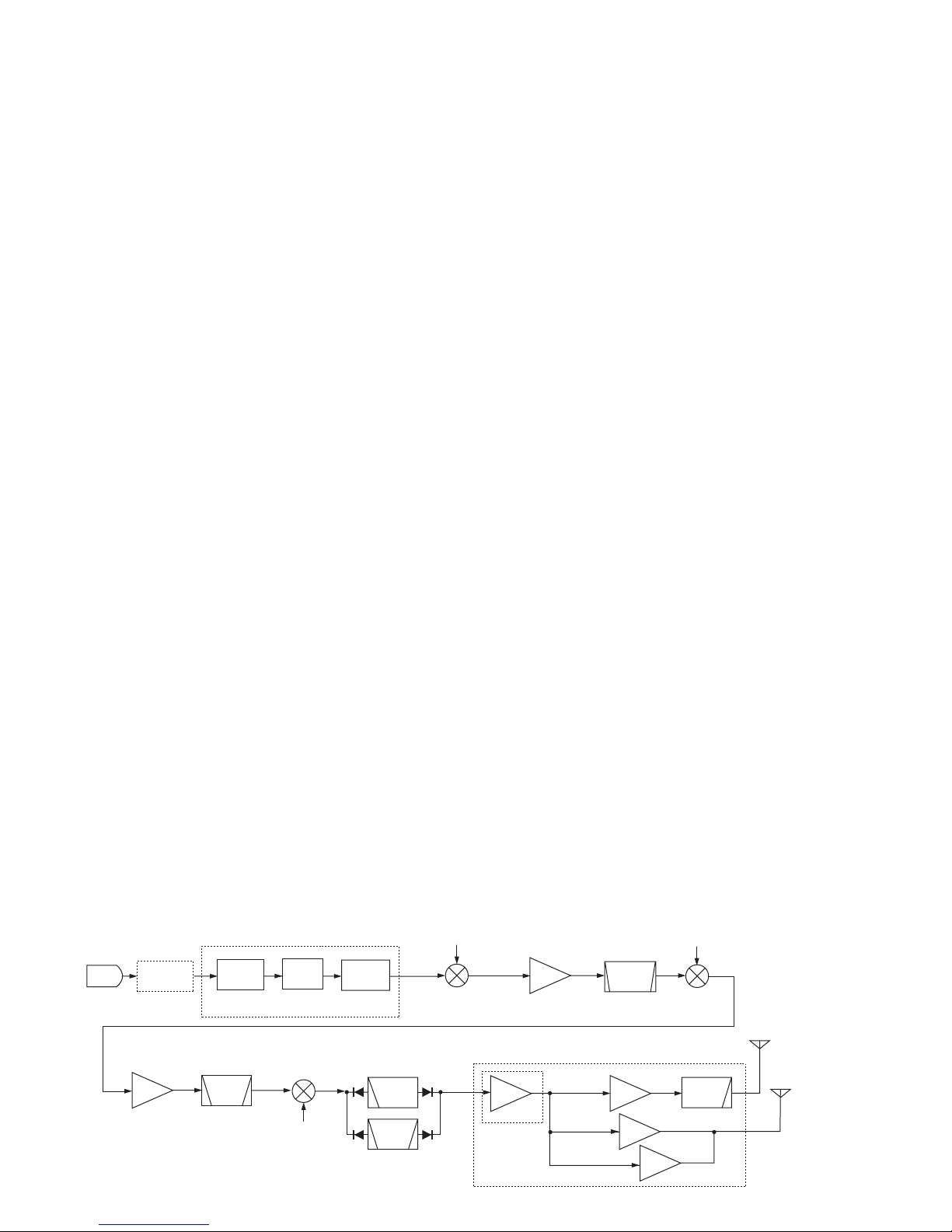
The amplified signals are passed through the band switch
(D461) and then applied to the 1st mixer circuit (MAIN unit)
via J101 (MAIN unit).
D453–D456, D553, D554, D556 and D558–D560 are
varactor diodes that tune the center frequency of an RF
passband for wide bandwidth receiving and good image
response rejection.
When receiving the signals, higher than 129 MHz, are
received, the switching diodes (D555, D557) are turned off
by the control signal “2MBL” from the CPU (LOGIC unit;
IC1302) via Q2150, then the varactor diodes (D556, D558)
are disconnected to shift the filtering frequencies.
3-1-3 PREAMPLIFIER CIRCUIT (MAIN UNIT)
The preamplifier circuit amplifies received RF signals for
wide band frequency range.
When the preamplifier is turned ON, the RF signals
(HF/50 MHz bands) from the high-pass filters are applied to
the preamplifier (Q301) via the preamplifier switches (D301,
D302).
When the preamplifier is turned OFF, the RF signals (HF/50
MHz bands) are passed through the bypass switches (D301,
D303).
The amplified or bypassed signals are applied to the 1st
mixer circuit (IC401).
3-1-4 1ST MIXER CIRCUIT (MAIN UNIT)
The 1st mixer circuit mixes the received RF signals with the
1st LO signal to convert the receive signal frequencies to
the 1st IF frequency.
While receiving the HF/50 MHz bands signals, the amplified
signals from the preamplifier switch (D304) or the bypassed
signals from the bypass switch (D303) are passed through
the low-pass filter (L310, L312, C314, C316, C318, C320,
C322) and then applied to the 1st mixer circuit (IC401) via
the band switch (D305).
While receiving the VHF/UHF bands signals, the signals
from the VHF/UHF RF circuit (PA unit) are passed through
the low-pass filter (L309, L311, L313, C313, C315, C317,
C319, C321, C323, C325) and then applied to the 1st mixer
circuit (IC401) via the band switch (D306).
The applied signals are mixed with the 1st LO signal (124.517
–594.487 MHz) and convert into the 1st IF signal.
The 1st LO signal is generated in the DDS unit, and applied
to the 1st mixer circuit (IC401, pins 1, 6) after being ampli-
fied and attenuated at the 1st LO amplifier (IC421, pins 1, 4)
and the attenuators (R416–R418, R421–R423), respectively.
The converted 1st IF signal is applied to the 1st IF circuit.
3-1-5 1ST IF CIRCUIT (MAIN UNIT)
The 1st IF circuit filters and amplifies the 1st IF signal.
The converted 1st IF signal is
applied to the IF amplifier (Q502)
via RX switches (D502, D505).
The 124.487 MHz 1st IF signal
(except WFM mode) passes
through the crystal filter (FI601)
via the mode switches (D602,
D604), and the 134.732 MHz 1st
IF signal (WFM mode) passes through the bandpass filter
(L607, L609, C602, C606, C608–C610, C617, C618) via the
mode switches (D601, D603) to suppress out-of-band sig-
nals.
Then the filtered signal is applied to the IF amplifier (Q702)
and then applied to the 2nd mixer circuit (D801) via the RX
switches (D702, D704).
3-1-6 2ND MIXER CIRCUIT (MAIN UNIT)
The 2nd mixer circuit mixes the 1st IF signal with the 2nd
LO signal to convert into the 2nd IF frequency.
The amplified signal from the IF amplifier (Q702) is applied
to the 2nd mixer circuit (D801) and then mixed with the 2nd
LO signal (124.032 MHz) to convert into the 455 kHz (other
than WFM) or 10.7 MHz (WFM) 2nd IF signal.
The 2nd LO signal is generated in the DDS unit, and applied
to the 2nd mixer circuit (D801) after being filtered and
attenuated at the low-pass filter (L808, C816, C817) and the
attenuators (R801, R805, R806, R809–R811), respectively.
The converted 2nd IF signal is applied to the 2nd IF circuit.
3-1-7 2ND IF CIRCUIT (MAIN UNIT)
The 2nd IF circuit amplifies and filters the 2nd IF signal.
The converted 2nd IF signal is applied to the bandpass filter
(FI901) to suppress undesired signals.
The 455 kHz 2nd IF signal (except
WFM mode) is passed through the
bandpass filter (FI901) via the mode
switch (D803) and then amplified
at the IF amplifier (Q902). The
amplified signal is passed through
the bandpass filter (FI1001) and
then applied to another IF amplifier
(Q1001).
The amplified signal is applied to the 3rd mixer circuit.
The 10.7 MHz 2nd IF signal for WFM mode is passed
through the low-pass filter (L1402, C1402–C1404) via
the mode switch (D802) and then applied to the IF ampli-
fier (Q1401). The amplified signal is passed through the
bandpass filter (FI1401) and then applied another IF ampli-
fier (Q1402).
3 - 2
• 1st IF frequency
Mode 1st IF
USB 124.48850 MHz
LSB 124.48550 MHz
CW 124.48700 MHz
RTTY 124.48683 MHz
AM/FM 124.48700 MHz
WFM 134.73200 MHz
• 2nd IF frequency
Mode 2nd IF
USB 456.500 kHz
LSB 453.500 kHz
CW 455.000 kHz
RTTY 454.830 kHz
AM/FM 455.000 kHz
WFM 10.700 MHz

3 - 3
The amplified IF signal is passed through the bandpass filter
(FI1402) and then applied to the WFM demodulator circuit
(IC1401).
3-1-8 3RD MIXER CIRCUIT (MAIN UNIT)
The 3rd mixer circuit mixes the 2nd IF signal with the 3rd LO
signal to convert into the 3rd IF frequency.
The amplified signal from the IF amplifier (Q1001) are mixed
with the 3rd LO signal (438.85 kHz), where come from the
DDS unit via J2406, at the 3rd mixer circuit (IC1101) to con-
vert into the 16.15 kHz 3rd IF signal.
The converted 3rd IF signal is applied to the 3rd IF circuit.
3-1-9 3RD IF CIRCUIT (MAIN UNIT)
The 3rd IF circuit filters and amplifies the 3rd IF signal.
The converted 3rd IF signal is amplified at the 3rd IF ampli-
fier (IC1203, pins 5, 7) and then passed through the low-
pass filter (IC1203, pins 1, 3). The filtered signal is passed
through the mode switches (IC1201, pins 1, 7; IC1202, pins
1, 7) and then applied to the analog switch (IC1256, pins 11,
13).
The switched signal is applied to the DSP circuit (LOGIC
unit) via the J2251 (pin 1).
3-1-10 DEMODULATOR CIRCUITS (MAIN UNIT)
• WFM mode
The demodulator circuit converts the 2nd IF signal into the
AF signals.
The filtered signal from the bandpass filter (FI1402) is
applied to the IF amplifier section inside the WFM demodu-
lator (IC1401, pin 1) and then applied to the quadrature
detector section to convert into AF signals. The detected AF
signals are output from pin 6 (IC1401) and then applied to
the mode switches (IC1201, pins 1, 7; IC1202, pins 1, 6).
The switched AF signals are applied to the analog switch
(IC1256, pins 11, 13) and then applied to the DSP circuit
(LOGIC unit) via J2251 (pin 1).
3-1-11 DSP CIRCUIT (LOGIC UNIT)
The DSP (Digital Signal Processor) circuit enables digital IF
filter, manual notch, digital twin PBT and phase demodula-
tion, etc.
The 3rd IF or demodulated AF (WFM mode) signals are
passed through the low-pass filter (IC451, pins 1, 2) and
then applied to the A/D converter (IC551, pin 4). The con-
verted signals are applied to the DSP ICs (IC301, IC2201)
for the digital IF filter, demodulation, automatic notch and
noise reduction, etc.
The output digital audio signals from the DSP IC (IC301) are
applied to the D/A converter (IC551) to convert into the ana-
log audio signals.
The converted audio signals from the D/A converter (IC551,
pins 25, 26) are passed through the low-pass filter (IC601,
pins 5–7), and then applied to the AF amplifier circuit (MAIN
unit) via J701 (pin 14).
3-1-12 AF AMPLIFIER CIRCUIT (MAIN UNIT)
The AF amplifier amplifies the demodulated AF signals to
drive speaker.
The filtered signal from the low-pass filter (LOGIC unit;
IC601, pins 5–7) are passed through another low-pass filter
(IC2551, pins 1, 3).
While in FM mode, the filtered AF signals from the low-pass
filter (IC2551, pin 1) are applied to the de-emphasis circuit
(IC2551, pins 5–7) to obtain the –6 dB/octave characteristics
and then applied to the AF switch (IC2601, pins 1, 6).
While except FM mode, the filtered AF signals from low-pass
filter (IC2551, pin 1) are applied to the AF switch (IC2601,
pins 1, 7).
The switched AF signals are amplified at the AF power
amplifier (IC2602, pins 1, 4) and then applied to the speaker
switch (Q2602).
The switched signal is applied to the internal speaker that is
connected to J2601 via [EXT SP] jack (J2602).
IC2551 IC2601 Q2602
IC2602
AF
IC2551
DSPO1
LOGIC UNIT MAIN UNIT
315 7
7
1
6
666
[EXT SP]
AF amp.
SP1
CHASSIS
LPF De-
emphasis
• AF CIRCUIT
LPF LPF
IC451
LOGIC unit
MAIN UNIT
CODEC IC (IC551)
IC301
IC601
DSPO2
AF
signals
DSPI2
(16.15 kHz)
3rd IF
signal
A/D
converter
D/A
converter
DSP IC
IC2201
DSP IC
• DSP CIRCUIT

3-1-13 AGC CIRCUIT (MAIN UNIT)
The AGC (Automatic Gain Control) circuit adjusts IF amplify
gain to keep the audio output at a constant level. The
receiver gain is determined by the voltage on the AGC line
from the DSP circuit.
The AGC voltage is detected at the AGC detector section
inside the DSP ICs (LOGIC unit; IC301, IC2201) and the
AGC voltage is applied to the D/A converter (IC2155). The
converted AGC voltage is applied to the IF amplifiers (Q702,
Q902, Q1001) after being amplified at IC1201 (pin 12) and
sets the receiver gain with [RF/SQL] control.
When receiving strong signals, the detected voltage increas-
es and the AGC voltage decreases. As the AGC voltage is
used for the bias voltage of the IF amplifiers (Q702, Q902,
Q1001), IF amplifier gain is decreased.
3-1-14 S-METER CIRCUIT (LOGIC UNIT)
The S-meter circuit indicates the relative received signal
strength while receiving.
The received signal strength is detected inside the DSP ICs
(IC301, IC2201) and then applied to the main CPU (IC1302).
The S-meter signal for WFM mode is output from the FM
detector IC (IC401, pin 4) and then applied to the to the
main CPU (IC1302, pin 123).
The S-meter signal from the main CPU (IC1302) is applied
to the sub CPU (DISPLAY unit; IC2003) and is then dis-
played on the LCD display.
3-1-15 SQUELCH CIRCUIT (MAIN UNIT)
The squelch circuit mutes audio output when the S-meter
signal is lower than the [RF/SQL] control setting level.
The S-meter signal from the DSP IC is applied to the main
CPU (LOGIC unit; IC1302) and is compared with the thresh-
old level set by the [RF/SQL] control. The [RF/SQL] setting
is picked up at the sub CPU (DISPLAY unit; IC2003, pin 74).
The main CPU (LOGIC unit; IC1302) compares the S-meter
signal and [RF/SQL] setting, and outputs the mute signal via
the DSP IC (IC301, pin B4) to the AF switch (IC2601, pin 2)
to cut AF signals via Q2607.
While receiving WFM mode, the S-meter signal is output
from the WFM demodulator (IC401, pin 4) and applied to the
to the main CPU (LOGIC unit; IC1302, pin 123). The main
CPU (LOGIC unit; IC1302) compares the S-meter signal and
[RF/SQL] setting, and outputs the mute signal via the DSP
IC (IC301, pin B4) to the AF switch (IC2601, pin 2) to cut AF
signals via Q2607.
3-2 TRANSMITTER CIRCUITS
3-2-1 MICROPHONE AMPLIFIER CIRCUIT (MAIN UNIT)
The microphone amplifier circuit amplifies microphone audio
signal to a level needed for the DSP circuit.
Audio signals from the [MIC] connector (FRONT unit; J303
or MAIN unit; J2003) are amplified at the microphone ampli-
fier (IC2007, pins 1, 2) and then applied to the DSP circuit
(LOGIC unit) via J2251 (pin 3).
3-2-2 DSP CIRCUIT (LOGIC UNIT)
The DSP (Digital Signal Processor) circuit enables digital
PSN modulator, digital Low Power modulator, digital Phase
modulator, transmitter monitor and side tone, etc.
The amplified microphone signals are passed through the
low-pass filter (IC502, pins 1, 2) and then applied to the A/D
converter (IC551, pin 3). The converted digital audio signal
are applied to the DSP ICs (IC301, IC2201) to covert into
the modulated 16.15 kHz 3rd IF signal. The modulated 3rd
IF signal from the DSP IC (IC301) is applied to the D/A con-
vertor (IC551) to convert into the analog 3rd IF signal. The
converted analog 3rd IF signal is output from pins 27, 28
(IC551) and then passed through the low-pass filter (IC601,
pins 1–3).
The filtered IF signal is applied to the 3rd mixer circuit (MAIN
unit) via the J701 (pin 12).
3-2-3 3RD MIXER CIRCUIT (MAIN UNIT)
The 3rd mixer circuit mixes the 3rd IF signal with the 3rd LO
signal to convert into the 2nd IF frequency.
The filtered signal from the low-pass filter (LOGIC unit;
IC601) is applied to the analog switch (IC2251, pins 1,
7) and then applied to the 3rd mixer circuit (IC1301, pins
3, 5). The applied signal is mixed with the 3rd LO signal
(438.85 kHz) coming from DDS unit via J2406 (pin 13) and
converted into the 455 kHz 2nd IF signal.
The converted 2nd IF signal is applied to the 2nd IF circuit.
3-2-4 2ND IF CIRCUIT (MAIN UNIT)
The 2nd IF circuit filters and amplifies the 2nd IF signal.
The converted 2nd IF signal is applied to the 2nd IF ampli-
fier (Q901) and then passed through the bandpass filter
(FI901) via the TX switch (D903) to suppress unwanted sig-
nals.
The filtered signal is applied to the 2nd mixer circuit.
3 - 4
DSP
CIRCUIT
IC301
IC2201
IC2101
3rd mixer 2nd mixer 1st mixer
IC2155
12
12 14
AGC
D/A
converter
IC1203
DSPI1 IF
amp.
Q1001IF
amp.
Q902 IF
amp.
Q702 From the
antenna
IF
amp.
Q502 IF
amp.
• AGC CIRCUIT

3-2-5 2ND MIXER CIRCUIT (MAIN UNIT)
The 2nd mixer circuit mixes the 2nd IF signal with the 2nd
LO signal to convert into the 1st IF frequency.
The filtered signal from the bandpass filter (FI901) is applied
to the 2nd mixer circuit (D801) and mixed with 2nd LO sig-
nal (124.032 MHz) to convert into the 1st IF signal.
The 2nd LO signal is generated in the DDS unit, and applied
to the 2nd mixer circuit (D801) after being filtered and
attenuated at the low-pass filter (L808, C816, C817) and the
attenuators (R801, R805, R806, R809–R811), respectively.
The converted 1st IF signal is applied to the 1st IF circuit.
3-2-6 1ST IF CIRCUIT (MAIN UNIT)
The 1st IF circuit amplifies and filters the 1st IF signal.
The converted 1st IF signal is applied to the IF amplifier
(Q701) via the TX switch (D703) and then passed through
the bandpass filter (FI601) to suppress unwanted signals via
the filter switches (D601, D602).
The filtered signals are applied to the 1st mixer circuit.
3-2-7 1ST MIXER CIRCUIT (MAIN UNIT)
The 1st mixer circuit mixes the 1st IF signal with the 1st LO
signal to convert into the RF frequency.
The filtered signal is applied to the 1st mixer circuit (IC401)
via the TX switches (D501, D504) and mixed with the 1st LO
signal (124.517–594.487 MHz) to convert into the RF signal.
The 1st LO signal is generated in the DDS unit, and applied
to the 1st mixer circuit (IC401, pins 1, 6) after being ampli-
fied and attenuated at the 1st LO amplifier (IC421, pins 1, 4)
and the attenuators (R416–R418, R421–R423), respectively.
The converted RF signal is applied to the RF circuit.
3-2-8 RF CIRCUIT (MAIN UNIT)
The RF circuit amplifies and filters the RF signal from the
1st mixer circuit.
The HF/50 MHz bands signal from the 1st mixer circuit
(IC401) is passed through the low-pass filter (L310, L312,
C314, C316, C318, C320, C322) via the band switch (D305).
The HF band signal is passed through one of 5 high-pass
(Refer to 3-1 for used RF high-pass filter) and low-pass
(L205, L207, C209–C213) filters.
The 50 MHz band signal is passed through the bandpass
filter (L219, L220, L246–L248, C240–C242, C282, C285–
C291).
The filtered HF/50 MHz bands signal is amplified at the YGR
amplifier (IC1) after passed through the high-pass filter (L109,
L110, L116, L117, C109, C114–C116) and attenuator (R5–
R7).
The amplified HF/50 MHz bands signal is applied to the
drive and power amplifier circuits (PA unit) via J1.
The VHF/UHF bands signal from the 1st mixer circuit (IC401)
is passed through the low-pass filter (L309, L311, L313,
C313, C315, C317, C319, C321, C323, C325) via the band
switch (D306).
The VHF band signal is passed through the bandpass filter
(L8, L10–L13, C18, C25, C26, C28, C29, C31–C33) via
the band switches (D3, D10) and then amplified at the RF
amplifier (IC2, pins 1, 3). The amplified signal is passed
through the band switch (D1) and attenuator (R5–R7), and
then applied to the YGR amplifier (IC1, pins 1, 4).
The amplified signal is passed through the high pass filter
(L21, C50–C52) via the filter switches (D6, D8) and then
applied to the drive and power amplifier circuits (PA unit) via
J1.
The UHF band signal is amplified at the RF amplifier (IC3,
pins 1, 3) via the band switch (D4) and passed through the
bandpass filters (FI2, FI3). The filtered signal is amplified at
the YGR amplifier (IC1, pins 1, 4) after passed through the
band switch (D2), attenuator (R5–R7) and bypass switches
(D7, D9).
The amplified signal is applied to the drive and power ampli-
fier circuits (PA unit) via J1.
3 - 5
• TRANSMITTER CONSTRUCTION
FI901
MIC BPF
Ceramic
455 kHz
3rd LO
(438.85 kHz)
IC2201 IC551
IC551 IC301
Controller A/D DSP
ICs D/A
FI601
BPF
Crystal
1st mixer
IC401
1st LO
(124.517−
594.487 MHz)
HPFs
BPF
IC504
LPFs
PA UNIT
LOGIC UNIT (DSP circuit)
MAIN UNIT DRIVER
UNIT
ANT1
ANT2
Q301
Q302
Q401
Q501
145 MHz
430 MHz
HF/50 MHz
Q901
AMP.
Q801
AMP.
2nd mixer
D801
2nd LO
(124.032 MHz)
124.487 MHz
AMP. PA
PA
PA

3 - 6
3-2-9 DRIVE AND POWER AMPLIFIER CIRCUITS
(PA AND DRIVER UNITS)
The drive and power amplifier circuits amplify the RF signal
from the RF circuit (MAIN unit) to obtain 100 W of RF output
power for the HF/50 MHz bands, 50 W for the VHF band
and 35 W for the UHF band.
The RF signal from the MAIN unit is applied to the pre drive
amplifiers (PA unit; Q101, Q102) after passed through the
attenuator (PA unit; R101–R103). The amplified signal is
applied to the drive amplifier (DRIVER unit; Q504) to amplify
a level needed for the power amplifiers.
The amplified HF/50 MHz bands signal from the drive ampli-
fier is amplified at the power amplifiers (PA unit; Q301,
Q302) to obtain a stable 100 W of RF output power. The
power amplified signal is passed through the TX/RX switch
(RL801), one of the 7 low-pass filters, APC detector (PA
unit; D961, D962) and then applied to the [ANT1] connector
(CHASSIS; J1).
The amplified VHF RF signal from the drive amplifier is
amplified at the power amplifier (Q501) to obtain a stable
50 W of RF output power. The power amplified signals are
applied to the low-pass filter, APC detector (D501–D504),
TX/RX switch (D506, D510), low-pass filters (L506, L508,
L510, L601–L603, C516, C519, C521, C601, C602) and
[ANT2] connector (CHASSIS; J2).
The amplified UHF RF signal from the drive amplifier is
amplified at the power amplifier (Q401) to obtain a stable
35 W of RF output power. The power amplified signal is
applied to the low-pass filter, APC detector (D401–D404),
TX/RX switch (D406, D407), high-pass filter (L413, L414,
C428, C429, C431, C433), low-pass filter (L601–L603,
C601, C602) and [ANT2] connector (CHASSIS; J2).
3-2-10 ALC CIRCUIT (MAIN UNIT)
The ALC (Automatic Level Control) circuit reduces the gain
of IF amplifiers in order for the transceiver to output a con-
stant RF power set by the RF power setting even when the
supplied voltage shifts, etc.
The HF/50 MHz power amplified signal from the power
amplifiers (PA unit; Q301, Q302) is detected at the APC
detector (PA unit; D961). The detected voltage is applied
to the buffer amplifier (PA unit; IC960, pins 5, 7) and then
applied to the MAIN unit as the “HFOR” voltage.
The VHF and UHF RF power amplified signal from the
power amplifiers (PA unit; Q401, Q501) are detected at the
APC detectors (PA unit; D401, D404, D501, D504) respec-
tively. The detected voltages ("VFOR" and "UFOR") are
combined to "VUFOR" voltage and then applied to the MAIN
unit.
The “HFOR” and “VUFOR” voltages are combined to the
“FORL” voltage and then applied to the ALC amplifier
(IC1601, pins 1, 2). The “POCV” voltage from the D/A con-
verter (IC2155, pin 19) via the buffer amplifier (IC2101,
pins 5, 7), determined by the RF power setting, is applied to
the ALC amplifier (IC1601, pin 3) as the reference voltage.
When the “FORL” voltage exceeds the “POCV” voltage, ALC
bias voltage from IC1601 (pin 1) controls the IF amplifiers
(Q701, Q901). This adjusts the output power to the level
determined by the RF power setting until the “FORL” and
“POCV” voltages are equalized.
In AM mode, IC1601 functions as an averaging ALC ampli-
fier with Q1601. The AM switch (Q1602) is turn ON and
shifts the “POCV” voltage to adjust the TX output power for
the AM mode (maximum; 40 W for HF/50 MHz bands, 20 W
for VHF band, 14 W for UHF band).
The ALC bias voltage from IC1601 is also applied to the
main CPU (LOGIC unit; IC1302, pin 115) as the “ALCL” volt-
age for ALC meter indication.
The external ALC input (negative voltage) from the [ACC]
socket (pin 6) is converted to a positive voltage at D1609
and is applied to the buffer amplifier (Q1604). External ALC
operation is identical to that of the internal ALC.
3-2-11 APC CIRCUIT (MAIN UNIT)
The APC (Automatic Power Control) circuit protects the
power amplifiers on the PA unit from high SWR and exces-
sive current.
The reflected wave signal appears and increases on the
antenna connector when the antenna is mismatched.
The HF/50 MHz reflected signal level is detected at D962 (PA
unit), and is amplified at the buffer amplifier (PA unit; IC960,
pins 1, 3) and applied to the ALC amplifier (IC1601, pins 8, 9)
as the "HREF" voltage.
IC1601
HF/50 MHz
145 MHz
430 MHz
2
1
HPFs LPFs
BPF
ALC
ALC amplifier
ANT1 ANT2
PA UNIT
DRIVER
UNIT
IF
ALC
FI601
Q701
Q901
TX
signals
Crystal
BPF
3rd mixer 2nd mixer 1st mixer
AMP PA
IF
PA
PA
APC
DET
APC
DET
APC
DET
• ALC CIRCUIT

The VHF/UHF APC detector circuits (PA unit; D501, D504,
D401, D404) detect the forward and reflection signals and
convert into DC voltages. The converted DC voltages are
combined and applied to the ALC amplifier (pins 1, 2) as
"VUFOR" voltage.
For the current APC, the driving current at the power ampli-
fiers is detected in the voltages (“ICH” and “ICL”) which
appear at both terminals of detector resistors (PA unit; R721,
R722). The detected voltages are applied to the APC ampli-
fier (IC1601, pins 5–7).
When the current of the power amplifier exceeds 22 A, The
output voltage from the APC amplifier (IC1601, pin 7) con-
trols the ALC line to prevent excessive current flow.
3-2-12 RF, ALC, SWR METER CIRCUITS (LOGIC UNIT)
While transmitting, RF, ALC or SWR meter readings are
available and can be selected with the [F3 (MET)] switch.
(1) Power meter
The “FOR,” “VFOR” and “UFOR” voltages are combined to
the “FORL” voltage, and it is then applied to the main CPU
(IC1302, pin 113) for indicating the TX output power.
(2) ALC meter
The ALC bias voltage from the buffer amplifier (MAIN unit;
IC1601, pin 14) is applied to the main CPU (IC1302, pin 115)
via the “ALCL” signal line for indicating the ALC level.
(3) SWR meter
The “FORL” and “REFL” voltages are applied to the main
CPU (IC1302, pins 113, 114) respectively. The main CPU
compares the ratio of “FORL” to “REFL” voltage and indi-
cates the SWR for the [ANT1] connector.
3-3 DDS CIRCUITS
3-3-1 GENERAL
The DDS unit generates a 1st LO (124.517–594.487 MHz),
a 2nd LO (124.032 MHz) and a 3rd LO (438.85 kHz) fre-
quencies.
3-3-2 1ST LO CIRCUIT (DDS UNIT)
The 1st LO circuit generates a 1st LO signal based on the
system clock that is tripled the 2nd LO frequency.
The 124.032 MHz 2nd LO signal is applied to the tripler
circuit (Q201) and then passed through the high-pass filter
(L205, L206, L210, C206–C210, C217–C219). The filtered
signal is amplified at Q211 and then passed through the
bandpass filter (FI201). The filtered signal is applied to the
DDS IC (IC301) as the 372.096 MHz system clock. The
DDS IC generates 38.62189–199.999999 MHz frequency
based on the system clock. The output signal from the DDS
IC (IC301, pins 20, 21) is applied to the doubler circuit
(D301) and then amplified at IC401 (pins 1, 4) after being
passed through the low-pass filter (L331, L332, C331, C332,
C335). The amplified signal is applied to one of the multiplier
circuits which is selected from the readout frequency and
then amplified at IC451 (pins 1, 5). The amplified signal is
passed through the bandpass filters.
The filtered signal is applied to the 1st mixer circuit (MAIN
unit) via J851.
3 - 7
124.517–
594.487 MHz
(1st LO) 124.032 MHz
(2nd LO)
24.8064 MHz
(system clock)
372.096 MHz
(system clock)
524.487–
594.487 MHz
124.517–
154.486999 MHz
154.487–
324.486999 MHz
[ANT1] [ANT2]
1st mixer
IC401
0.03–
60 MHz
60–
470 MHz
438.85 kHz
(3rd LO)
IC51
IC301
Q101
FI101
IC61
×5
DDS UNIT
MAIN UNIT
DDS
BPF
2nd mixer
D801
3rd mixer
IC1101
1st IF: 124.487 MHz
(WFM: 134.732 MHz)
to DSP circuit
Ref. Osc.
24.8064 MHz
LPF
2nd IF: 455 kHz 3rd IF: 16.15 kHz
Q1
to WFM detector
(IC1401)
×2
×3
×2 BPF
D456
BPF
×4 BPF
D471
FI201 Q201
Q
301
BPF
DDS
X1
AMP.
AMP.
• FREQUENCY CONSTRUCTION

3-5 POWER SUPPLY CIRCUITS
3-5-1 FRONT UNIT VOLTAGE LINE
Line Description
3.3 V
Common 3.3 V converted from the 5 V line
by the 3.3 V regulator circuit (IC151). The out-
put voltage is applied to the sub CPU (IC2003),
etc.
5 V
Common 5 V converted from the 8 V line by
the 5 V regulator circuit (IC101). The output
voltage is applied to the LCD driver (IC506),
etc.
3-3-3 2ND LO AND REFERENCE OSCILLATOR
CIRCUITS (DDS UNIT)
The reference oscillator (X1, Q1) generates a 24.8064 MHz
frequency used for the 1st LO, 3rd LO and DSP circuits as a
system clock and for the 2nd LO signal.
The oscillated signal is multiplied by 5 at Q101 and then
passed through the bandpass filter (FI101). The filtered
124.032 MHz signal is amplified at Q151 and then applied to
the 2nd mixer circuit (MAIN unit) after being passed through
the low-pass filter (L153, C154–C156) and attenuator (R157
–R159) via J151 as the 2nd LO signal.
3-3-4 3RD LO CIRCUIT (DDS UNIT)
The 3rd LO circuit generates a 3rd LO signal and shift the
frequency for the operating mode needed.
The DDS IC (IC51) generates a 10-bit digital signal. The
24.8064 MHz system clock signal from the reference oscil-
lator (X1, Q1) is buffer amplified at IC61 (pins 2, 4) and then
applied to DDS IC (IC51, pins 5, 10). The DDS IC (IC51)
generates the 438.85 kHz frequency signal and then output
from pin 10. The output signal is applied to the low-pass fil-
ter (L53, C59–C61) and then applied to the 3rd mixer circuit
(MAIN unit) via J952 (pin 13) as the 3rd LO signal.
• 3RD LO FREQUENCY
Mode RX frequency
[kHz]
TX frequency
[kHz]
USB 440.350 440.350
LSB 437.350 437.350
CW 438.850
(–CW PITCH) 438.850
CW-R 438.850
(+CW PITCH) 438.850
RTTY 436.555* 436.555*
RTTY-R 440.975* 436.555*
AM 438.850 438.850
FM 438.850 438.850
*RTTY TONE: 2125 Hz, RTTY SHIFT: 170 Hz
3-4 LOGIC CIRCUITS
3-4-1 BAND SELECTION DATA
Frequency
[MHz]
IC2151
(MAIN)
IC2152
(MAIN)
IC2152
(MAIN)
IC981
(PA)
IC901
(DDS)
HPF
(MAIN) LPF (PA) LOF
(DDS)
0.03–1.599999 B0 L1
LOF1
1.6–1.999999 B1
2.0–3.399999 B2 L2
3.4–3.999999 B3
4.0–6.899999 L3
6.9–7.300000
B4
7.300001–7.999999
L4
8.0–10.999999
11.0–13.899999
13.9–14.350000
B5
14.350001–
14.999999 L5
15.0–20.899999
20.9–21.45
B6
21.450001–
21.999999 L6
22.0–29.999999
30.0–49.999999 T: B1
R: B7
L7 LOF250.0–54.0 B7
54.000001–
59.999999
T: B1
R: B7
60.0–115.512999
L8 L8
LOF3
115.513–
128.999999 LOF4
129.0-148.0
148.000001–
199.999999 LOF5
400.0–470.0 L9 L9 LOF6
3 - 8

3-5-2 MAIN UNIT VOLTAGE LINE
Line Description
3.3 V
Common 3.3 V converted from the 5 V line
by the 3.3 V regulator circuit (IC1801). The
output voltage is applied to the D/A convert-
er ICs (IC2151–IC5155), etc.
5 V
Common 5 V converted from the H V line by
the 5 V regulator circuit (IC1951). The output
voltage is applied to the CODEC IC (LOGIC
unit; IC551), low-pass filters (LOGIC unit;
IC451, IC502), etc.
8 V
Common 8 V line converted from the HV
line by the 8 V regulator circuit (IC1901).
The output voltage is applied to the buffer
amplifiers (IC2101–IC2103), analog switches
(IC2156, IC2251), etc.
T8
Transmit 8 V controlled by the T8 regulator
circuit (Q1703, Q1704) using TXS signal
from the CPU (LOGIC unit; IC1302, pin
106). The output voltage is applied to the RF
switch (Q101), 2nd IF amplifier (Q701), 3rd
IF amplifier (Q901), etc.
R8
Receive 8 V controlled by the R8 regulator
circuit (Q1701, Q1702) using RXS signal
from the CPU (LOGIC unit; IC1302, pin 105).
The output voltage is applied to the 2nd IF
amplifier (Q702), 3rd IF amplifier (Q1001),
3rd mixer (Q1101), etc.
3 - 9
3-6 PORT ALLOCATIONS
3-6-1 SUB-CPU (DISPLAY UNIT; IC2003)
Pin
number
Port
name Description
3, 5 MDBK,
MDAK Input ports for [DIAL].
13, 14 S1AK,
S1BK Input ports for [PBT2/M-ch] control.
15, 16 S2AK,
S2BK Input ports for [PBT1/RIT] control.
21 VRK Input port for [AF] switch.
22 PBTK Input port for [PBT/M-ch] switch.
23 TUNK Input port for [TUNER/CALL] key.
24 TSK Input port for [TS] key.
25 LCKK Input port for [LOCK] key.
26 BUPK Input port for [Y(BAND)] key.
27 BDNK Input port for [Z(BAND)] key.
28 FMSL Input port for the HM-151 connection
detection.
35 PHNK Input port for the headphones
connection detection.
37 LCK Outputs clock signal for the LCD driv-
er (IC506).
Pin
number
Port
name Description
38 LDT Outputs data signal for the LCD driver
(IC506).
39 LDST Outputs strobe signal for the LCD
driver (IC506).
47 FSQS Outputs the squelch control signal.
High: Squelch is opened.
48 RXD
Outputs the RX LED control signal.
High: While receiving or squelch is
opened.
54 BLV Outputs the dimmer control signal for
the LCD backlights.
55 KLV Outputs the dimmer control signal for
the key backlights.
56 TXD Outputs TX LED control signal.
Low : While transmitting.
57 PBT1D
Outputs control signal for [PBT/M-ch/
RIT] indicator.
Low : While the RIT function is ON.
58 PBT2D
Outputs control signal for [PBT/M-ch/
RIT] indicator.
Low : While the PBT function is ON.
70 LRXD Input port for data signal from the
main CPU (LOGIC unit; IC1302).
71 LTXD Outputs data signal to the main CPU
(LOGIC unit; IC1302).
73 AFGL Input port for [AF] control.
74 SQLL Input port for [RF/SQL] control.
75 PTTL
Input port for PTT control signal from
the microphone that is connected to
the FRONT unit.
77 FUDL
Input port for [UP] and [DN] switch-
es from the optional microphone
(HM-103, SM-20) that is connected to
the FRONT [MIC] connector.
78 KI0L
Input port for [MODE], [P.AMP/ATT],
[Y(MENU/GRP)] and [Z(MENU/
GRP)] keys.
79 KI1L Input port for [F-1], [F-2], [F-3] and
[F-4] keys.
80 KI2L Input port for [NB LEV], [NR LEV], [N/
ANF] and [SET/REC] keys.

3 - 10
3-6-2 MAIN CPU (LOGIC UNIT; IC1302)
Pin
number
Port
name Description
26 CYDT Outputs data signal for the clock gen-
erator (IC1201) for display control.
27 CYCK Outputs clock signal for the clock gen-
erator (IC1201) for display control.
29 RTCDT
I/O port for the data signal from/to the
clock IC (IC1304) for clock indication
and timer function.
30 RTCCK
Outputs clock signal for the clock IC
(IC1304) for clock indication and timer
function.
42 LOST Outputs strobe signal for the D/A con-
verter (DDS unit; IC901).
43 MST
Outputs strobe signal for the D/A
converter ICs (MAIN unit; IC2151–
IC2154).
46 MMDK
Input port for the data signal from the
microphone that is connected to the
rear [MIC] connector.
47 DRES Outputs the reset signal for the DSP
ICs (IC301, IC2201).
48 PRES#
Outputs the reset signal for the LCD
controller (IC1226) and DDS IC (DDS
unit; IC301).
49 SQSS
Outputs the squelch control signal for
the ACC connector and connected
microphone.
51 MCK
Outputs clock signal for the D/A
converter ICs (MAIN unit; IC2151–
IC2154).
52 MDT
Outputs serial data signal for the D/A
converter ICs (MAIN unit; IC2151–
IC2154).
57 SDSS
Outputs the signal for H SEND or V
SEND selection.
High: While V SEND is selected.
58 TDAT • Outputs data signal for AT-180.
• Outputs start signal for AH-3/AH-4.
81 DTXD Outputs data signal for the DSP IC
(IC301).
82 DRXD Input port for data signal from the
DSP IC (IC301).
83 2T8V
Outputs the TX band signal.
High: While transmitting the 144 MHz
band.
104 4T8V
Outputs the TX band signal.
High: While transmitting the 430 MHz
band.
105 RXS
Outputs R8 regulator (Q1701, Q1702)
control signal.
Low : While receiving.
106 TXS
Outputs T8 regulator (Q1703, Q1704)
control signal.
Low :While transmitting.
107 POWS Outputs the power control signal .
High:When IC-7000 is power ON.
Pin
number Port name Description
109 ECK Outputs clock signal to the EE-
PROM (IC1301).
110 EDT I/O port for the EEPROM (IC1301).
113 FORL Input port for the forward voltage.
114 REFL Input port for the reflection voltage .
115 ALCL Input port for ALC level.
116 SNDL
Input port for PTT control signal
from the FRONT unit or ACC con-
nector.
117 DPTL Input port for PTT control signal
from the DATA connector.
118 THML Input port for the temperature de-
tection signal.
119 MUDL
Input port for [UP] and [DN] switch-
es from the optional microphone
(HM-103, SM-20) that is connected
to the rear [MIC] connector.
121,
122
DASK,
DOTK Input ports for [KEY] jack.
124 MMSL Input port for the HM-151 connec-
tion detection.
127 TKEY Input port for tuner ON.
128 TRD Input port for the detected signal for
the tuner unit connection.
133 LTXD Outputs data signal to the sub CPU
(DISPLAY unit; IC2003).
134 LRXD Inputs data signal from the sub
CPU (DISPLAY unit; IC2003).
135 PWRK Input port for [PWR] key.
Low : While [PWR] key is pushed.
137 3DST
Outputs strobe signal to the DDS
IC (DDS unit; IC51) for the 3rd LO
signal.
138 PCK
Outputs clock signal for the DDS
ICs (DDS unit; IC51, IC301) and
D/A converter (DDS unit; IC901).
140 1DST
Output strobe signal to the DDS IC
(DDS unit; IC301) for the 1st LO
signal.
142 PDT
Outputs serial data signal for the
DDS ICs (DDS unit; IC51, IC301)
and D/A converter (DDS unit;
IC901).

2-conductor 3.5 (d) mm (1⁄8″) plug
to [REMOTE] jack
Rear panel
Front panel
JIG plug
Shorten the both terminals
[P.AMP/ATT]
[TUNER/CALL]
[PWR]
KEY ACC DATA MIC
ANT2 ANT1
DC 13.8V
GND
4 - 1
SECTION 4 ADJUSTMENT PROCEDURES
4-1 PREPARATION
Some adjustment must be performed on the adjustment mode.
M REQUIRED TEST EQUIPMENT
EQUIPMENT GRADE AND RANGE EQUIPMENT GRADE AND RENGE
DC power supply Output voltage : 13.8 V DC
Current capacity : 30 A or more Distortion meter Frequency range : 1 kHz ±10 %
Measuring range : 1–100 %
RF power meter
(treminated type)
Measuring range : 0.5–200 W
Frequency range : 1.8–500 MHz
Impedance : 50 Ω
SWR : 1.2 : 1 or better
Oscilloscope Frequency range : DC–100 MHz
Measuring range : 0.01–10 V
Digital multimeter Imput impeadance : 10 MΩ/DC or more
AC millivoltmeter Measuring range : 10 mV to 10 V
Frequency counter
Frequency range : 0.1–500 MHz
Frequency accuracy : ±1 ppm or better
Sensitivity : 100 mV or better
DC voltmeter Input impedance : 50 kΩ/V DC or more
DC ammeter Measuring capability : 5 A/30 A
RF voltmeter Frequency range : 0.1–500 MHz
Measuring range : 0.01–10 V Audio generator Frequency range : 300–3000 Hz
Measuring range : 1–500 mV
Standard signal
generator (SSG)
Frequency range : 0.1–500 MHz
Output level : 0.1 µV to 32 mV
(–127 to –17 dBm)
External speaker Input impedance : 8 Ω
Capacity : 5 W or more
MENTERING THE ADJUSTMENT MODE
q Turn the transceiver’s power OFF.
w Connect the JIG plug (see illustration below) to [REMOTE] jack on the rear panel.
e While pushing and holding [P.AMP/ATT] and [TUNE/CALL], turn the transceiver power ON.
NOTE: Exiting from the adjustment mode when the transceiver's power is OFF.
MOPERATING ON THE ADJUSTMENT MODE
• Enter DDS adjustment mode. : Push [F-1 (REF)]
• Enter TX adjustment mode. : Push [F-2 (TX)]
• Enter RX adjustment mode. : Push [F-3 (RX)]
• Store the set value. : Push [F-4 (SET)]
• Adjust the value. : Rotate [DIAL]
CAUTION: Connect a dummy load to the antenna con-
nectors during the transmitter adjustment,
when the adjustment condition does not re-
quire a test equipment.
[F-1(REF)] [F-3 (RX)]
[DIAL]
[F-2 (TX)] [F-4 (SET)]

Audio
generator
RF power meter
A200 W/50 Ω
DC power supply
AA13.8 V/30 A Standard signal
aagenerator
AC
millivoltmeter
CAUTION!
DO NOT connect the
signal generator while
transmitting.
Speaker
to [EXT SP]
to [MIC]
to [DC 13.8 V]
to [ANT 1/2]
• Microphone connector (Rear panel view)
Frequency counter
Ammeter
5 A, 30 A
Pin 5
MIC GND
Pin 6
MIC INPUT
–
+
Pin 4
PTT
Millivoltmerter
18
Pin 7
GND
–
+
NOTE! Connect the test equipment to the
micropho0ne connector on the rear panel,
otherwise the transmitter adjustment will not
adjusted properly.
4 - 2
• CONNECTION

4-3 DISPLAY ADJUSTMENT
ADJUSTMENT ADJUSTMENT CONDITION MEASUREMENT VALUE ADJUSTMENT
UNIT LOCATION UNIT ADJUST
DISPLAY 1 • Connect between DISPLAY unit
ground and MAIN unit ground.
• Disconnect J2231 (MAIN unit).
• Receiving
DIS-
PLAY
Connect a frequency
counter to CP536
through a capacitor
(0.0047 µF) and resistor
(1 kΩ) in series.
3.579545 MHz
[USA]
4.433619 MHz
[Others]
DIS-
PLAY
C536
2 • Receiving Connect a frequency
counter to CP505.
15.734 kHz
[USA]
15.625 kHz
[Others]
DIS-
PLAY
R541
After the adjustment, connect J2231 (MAIN unit) and disconnect jumper wire between DISPLAY unit ground
and MAIN unit ground.
4 - 3
4-2 DDS ADJUSTMENT
ADJUSTMENT ADJUSTMENT CONDITION DISPLAY OPERATION
REFERENCE
FREQUENCY
1 • Enter the adjustment mode.
• Push [F1 (REF)].
2•Disconnect P4 from J801 (MAIN
unit).
• Receiving
REF OSC Connect a frequency counter to P4 and
set 124.032000 MHz using [DIAL]. Then
push [F-4 (SET)].
After the adjustment, exit the adjustment mode and connect P4 to J801 (MAIN unit).
4-4 TRANSMITTER ADJUSTMENT
ADJUSTMENT ADJUSTMENT CONDITION DISPLAY OPERATION
DRIVE/FINAL
IDLING
CURRENT
1 • Enter the adjustment mode.
• Push [F-2 (TX)].
2•Connect an RF power meter to
[ANT1] and [ANT2] connectors.
• Apply no audio signals to [MIC]
jack.
• Connect a DC ammeter (5 A
type) between power supply and
transceiver.
• Transmitting
Driver Idle Cur Preset the adjustment value to "00" using
with [DIAL], and check the driving current.
3 Rotate [DIAL] to set adjustment value to
1 A value from the driving current of "00"
value. Then push [F-4 (SET )].
4Final Idle Cur(HF/50M)-1 Preset the adjustment value to "00" using
with [DIAL], and check the driving current.
5 Rotate [DIAL] to set adjustment value to
1 A value from the driving current of "00"
value. Then push [F-4 (SET )].
6Final Idle Cur(HF/50M)-2 Preset the adjustment value to "00" using
with [DIAL], and check the driving current.
7 Rotate [DIAL] to set adjustment value to
1 A value from the driving current of "00"
value. Then push [F-4 (SET )].
8Final Idle Cur(144M) Preset the adjustment value to "00" using
with [DIAL], and check the driving current.
9 Rotate [DIAL] to set adjustment value to
2 A value from the driving current of "00"
value. Then push [F-4 (SET )].
10 Final Idle Cur(430M) Preset the adjustment value to "00" using
with [DIAL], and check the driving current.
11 Rotate [DIAL] to set adjustment value to
2.5 A value from the driving current of
"00" value. Then push [F-4 (SET )].
After the adjustment, exit the adjustment mode.

CP536
Display check point
R541
Display adjustment point
Display check point
CP505
Display adjustment point
Frequency
counter
C536
0.0047µF 1kΩ
4 - 4
• FRONT UNIT
• MAIN UNIT
J2231
Display adjustment
presetting
P4
Reference frequency
check point
J801
Ammeter
DC power
supply
Rear panel view

4 - 5
4-4 TRANSMITTER ADJUSTMENT (continue)
ADJUSTMENT ADJUSTMENT CONDITION MEASUREMENT VALUE ADJUSTMENT
UNIT LOCATION UNIT ADJUST
SWR
DETECTOR
1 • Operating freq : 10.10000 MHz
• MODE : USB
• RF Power : 100%
• MIC Gain : 50%
• Connect an audio generator to
[MIC] connector and set as;
Frequency : 1.5 kHz
• Connect a wire between CP1601
(MAIN unit) and ground.
• Transmitting
REAR
panel
Connect an RF power
meter to [ANT1] connec-
tor.
80 W Audio
genera-
tor
Output
level
2 PA Connect a DC voltmeter
to CP961.
Minimum volt-
age
PA C964
After adjustment, disconnect the wire between CP1601 (MAIN unit) and ground.
TX PEAK 1 REAR
panel
Connect an RF power
meter to [ANT1] connec-
tor.
Maximum out-
put power
MAIN L701
• Operating freq. : 10.10000 MHz
• MODE : USB
• RF Power : 100%
• MIC Gain : 50%
• Preset R1618 (MAIN
unit) as the illustration at
right.
• Preset L604, L612
and L904 (MAIN
unit) as the illustra-
tion at right.
• Connect an audio generator to
[MIC] connector and set as ;
Level : 1.5 kHz/3 mV
(Adjust the audio generator
output level to keep less than
50 W output power.)
• Transmitting
ADJUSTMENT ADJUSTMENT CONDITION DISPLAY OPERATION
TX TOTAL
GAIN
1 • Enter the adjustment mode.
• Push [F-2 (TX)].
2•Connect an RF power meter to
[ANT1] connector.
• Connect an audio generator to
[MIC] connector and set as;
Level : 1.5 kHz/3 mV
• Transmitting
TX Total Gain(HF1)
Set the output power to 50 W using
[DIAL]. Then push [F-4 (SET)].
3
TX Total Gain(HF2)
Set the output power to 50 W using
[DIAL]. Then push [F-4 (SET)].
4
TX Total Gain(HF3)
Set the output power to 50 W using
[DIAL]. Then push [F-4 (SET)].
5
TX Total Gain(50M)
Set the output power to 50 W using
[DIAL]. Then push [F-4 (SET)].
6•Connect an RF power to [ANT2]
connector.
• Transmitting
TX Total Gain(144M)
Set the output power to 25 W using
[DIAL]. Then push [F-4 (SET)].
7
TX Total Gain(430M)
Set the output power to 17.5 W using
[DIAL]. Then push [F-4 (SET)].
Core’s
top
Other manuals for IC-7000
9
Table of contents
Other Icom Transceiver manuals
Popular Transceiver manuals by other brands

ADTRAN
ADTRAN T200 FNID Installation and Maintenance

Microwave Data Systems
Microwave Data Systems MDS 4310 Installation, Operation & Field Maintenance

City Theatrical
City Theatrical Multiverse Vero 7400-5903 user manual

Galaxy
Galaxy DX-55V owner's manual

Alinco
Alinco DJ-V17TFH instruction manual

Azden
Azden pcs5000 instruction manual