Icom IC-7400 User manual

HF/VHF TRANSCEIVER
i7400
SERVICE
MANUAL

VERSION
Europe
France
Italy
Spain
Korea
SYMBOL
EUR
FRA
ITR
ESP
KOR
INTRODUCTION
This service manual describes the latest service information
for the IC-7400 HF/VHF TRANSCEIVER.
DANGER
NEVER connect the transceiver to an AC outlet or to a DC
power supply that uses more than 16 V. This will ruin the
transceiver.
DO NOT expose the transceiver to rain, snow or any liquids.
DO NOT reverse the polarities of the power supply when
connecting the transceiver.
DO NOT apply an RF signal of more than 20 dBm (100 mW)
to the antenna connector. This could damage the transceiv-
er’s front end.
ORDERING PARTS
Be sure to include the following four points when ordering
replacement parts:
1. 10-digit order numbers
2. Component part number and name
3. Equipment model name and unit name
4. Quantity required
<SAMPLE ORDER>
1110003870 S.IC NJM2058M-T1 IC-7400 MAIN UNIT 5 pieces
8810005770 Screw BiH M3 × 8 ZK IC-7400 Top cover 10 pieces
Addresses are provided on the inside back cover for your
convenience.
REPAIR NOTES
1. Make sure a problem is internal before disassembling the
transceiver.
2. DO NOT open the transceiver until the transceiver is
disconnected from its power source.
3. DO NOT force any of the variable components. Turn
them slowly and smoothly.
4. DO NOT short any circuits or electronic parts. An insu-
lated tuning tool MUST be used for all adjustments.
5. DO NOT keep power ON for a long time when the trans-
ceiver is defective.
6. DO NOT transmit power into a signal generator or a
sweep generator.
7. ALWAYS connect a 50 dB to 60 dB attenuator between
the transceiver and a deviation meter or spectrum ana-
lyzer when using such test equipment.
8. READ the instructions of test equipment thoroughly
before connecting equipment to the transceiver.
VER. NO.
#03
#04
#08
#09
#10
To upgrade quality, any electrical or mechanical parts and
internal circuits are subject to change without notice or
obligation.
for
free
by
RadioAmateur.eu

TABLE OF CONTENTS
SECTION 1 SPECIFICATIONS
SECTION 2 INSIDE VIEWS
SECTION 3 DISASSEMBLY AND OPTION INSTALLATIONS
SECTION 4 CIRCUIT DESCRIPTION
4 - 1 RECEIVER CIRCUITS . . . . . . . . . . . . . . . . . . . . . . . . . . . . . . . . . . . . . . . . . . . . . . . . . . . . . . . . . . . . 4 - 1
4 - 2 TRANSMITTER CIRCUITS . . . . . . . . . . . . . . . . . . . . . . . . . . . . . . . . . . . . . . . . . . . . . . . . . . . . . . . . .4 - 4
4 - 3 PLL CIRCUITS . . . . . . . . . . . . . . . . . . . . . . . . . . . . . . . . . . . . . . . . . . . . . . . . . . . . . . . . . . . . . . . . . 4 - 6
4 - 4 ANTENNA TUNER CIRCUITS . . . . . . . . . . . . . . . . . . . . . . . . . . . . . . . . . . . . . . . . . . . . . . . . . . . . . . 4 - 7
4 - 5 POWER SUPPLY CIRCUITS . . . . . . . . . . . . . . . . . . . . . . . . . . . . . . . . . . . . . . . . . . . . . . . . . . . . . . . 4 - 8
SECTION 5 ADJUSTMENT PROCEDURES
5 - 1 PREPARATION BEFORE SERVICING . . . . . . . . . . . . . . . . . . . . . . . . . . . . . . . . . . . . . . . . . . . . . . . 5 - 1
5 - 2 PLL ADJUSTMENTS . . . . . . . . . . . . . . . . . . . . . . . . . . . . . . . . . . . . . . . . . . . . . . . . . . . . . . . . . . . . . 5 - 2
5 - 3 TRANSMITTER ADJUSTMENTS . . . . . . . . . . . . . . . . . . . . . . . . . . . . . . . . . . . . . . . . . . . . . . . . . . . . 5 - 4
5 - 4 RECEIVER ADJUSTMENTS . . . . . . . . . . . . . . . . . . . . . . . . . . . . . . . . . . . . . . . . . . . . . . . . . . . . . . . 5 - 8
5 - 5 ADJUSTMENT MODE . . . . . . . . . . . . . . . . . . . . . . . . . . . . . . . . . . . . . . . . . . . . . . . . . . . . . . . . . . . 5 - 10
SECTION 6 PARTS LIST
SECTION 7 MECHANICAL PARTS
SECTION 8 SEMI-CONDUCTOR INFORMATION
SECTION 9 BOARD LAYOUTS
9 - 1 S-LOGIC BOARD . . . . . . . . . . . . . . . . . . . . . . . . . . . . . . . . . . . . . . . . . . . . . . . . . . . . . . . . . . . . . . . 9 - 1
9 - 2 DISPLAY BOARD . . . . . . . . . . . . . . . . . . . . . . . . . . . . . . . . . . . . . . . . . . . . . . . . . . . . . . . . . . . . . . . 9 - 3
9 - 3 TEN-KEY BOARD . . . . . . . . . . . . . . . . . . . . . . . . . . . . . . . . . . . . . . . . . . . . . . . . . . . . . . . . . . . . . . . 9 - 5
9 - 4 MODE BOARD . . . . . . . . . . . . . . . . . . . . . . . . . . . . . . . . . . . . . . . . . . . . . . . . . . . . . . . . . . . . . . . . . 9 - 5
9 - 5 PHONE BOARD . . . . . . . . . . . . . . . . . . . . . . . . . . . . . . . . . . . . . . . . . . . . . . . . . . . . . . . . . . . . . . . . 9 - 5
9 - 6 RIT BOARD . . . . . . . . . . . . . . . . . . . . . . . . . . . . . . . . . . . . . . . . . . . . . . . . . . . . . . . . . . . . . . . . . . . . 9 - 5
9 - 7 PBT BOARD . . . . . . . . . . . . . . . . . . . . . . . . . . . . . . . . . . . . . . . . . . . . . . . . . . . . . . . . . . . . . . . . . . . 9 - 5
9 - 8 MIC BOARD . . . . . . . . . . . . . . . . . . . . . . . . . . . . . . . . . . . . . . . . . . . . . . . . . . . . . . . . . . . . . . . . . . . 9 - 6
9 - 9 MAIN UNIT . . . . . . . . . . . . . . . . . . . . . . . . . . . . . . . . . . . . . . . . . . . . . . . . . . . . . . . . . . . . . . . . . . . . 9 - 7
9 - 10 DSP UNIT . . . . . . . . . . . . . . . . . . . . . . . . . . . . . . . . . . . . . . . . . . . . . . . . . . . . . . . . . . . . . . . . . . . . . 9 - 9
9 - 11 RF UNIT . . . . . . . . . . . . . . . . . . . . . . . . . . . . . . . . . . . . . . . . . . . . . . . . . . . . . . . . . . . . . . . . . . . . . 9 - 11
9 - 12 CTRL UNIT . . . . . . . . . . . . . . . . . . . . . . . . . . . . . . . . . . . . . . . . . . . . . . . . . . . . . . . . . . . . . . . . . . . 9 - 13
9 - 13 TUNER UNIT . . . . . . . . . . . . . . . . . . . . . . . . . . . . . . . . . . . . . . . . . . . . . . . . . . . . . . . . . . . . . . . . . . 9 - 15
9 - 14 PA UNIT . . . . . . . . . . . . . . . . . . . . . . . . . . . . . . . . . . . . . . . . . . . . . . . . . . . . . . . . . . . . . . . . . . . . . 9 - 17
9 - 15 FILTER UNIT . . . . . . . . . . . . . . . . . . . . . . . . . . . . . . . . . . . . . . . . . . . . . . . . . . . . . . . . . . . . . . . . . . 9 - 19
9 - 16 DRV BOARD . . . . . . . . . . . . . . . . . . . . . . . . . . . . . . . . . . . . . . . . . . . . . . . . . . . . . . . . . . . . . . . . . . 9 - 19
9 - 17 VARISTOR-A BOARD . . . . . . . . . . . . . . . . . . . . . . . . . . . . . . . . . . . . . . . . . . . . . . . . . . . . . . . . . . . 9 - 19
9 - 18 VARISTOR-B BOARD . . . . . . . . . . . . . . . . . . . . . . . . . . . . . . . . . . . . . . . . . . . . . . . . . . . . . . . . . . . 9 - 19
9 - 19 VARISTOR-C BOARD . . . . . . . . . . . . . . . . . . . . . . . . . . . . . . . . . . . . . . . . . . . . . . . . . . . . . . . . . . . 9 - 19
9 - 20 VARISTOR-D BOARD . . . . . . . . . . . . . . . . . . . . . . . . . . . . . . . . . . . . . . . . . . . . . . . . . . . . . . . . . . . 9 - 19
SECTION 10 BLOCK DIAGRAM
SECTION 11 WIRING DIAGRAM
SECTION 12 VOLTAGE DIAGRAMS
12 - 1 DSP UNIT . . . . . . . . . . . . . . . . . . . . . . . . . . . . . . . . . . . . . . . . . . . . . . . . . . . . . . . . . . . . . . . . . . . . 12 - 1
12 - 2 FRONT UNIT . . . . . . . . . . . . . . . . . . . . . . . . . . . . . . . . . . . . . . . . . . . . . . . . . . . . . . . . . . . . . . . . . . 12 - 2
12 - 3 MAIN UNIT (1) . . . . . . . . . . . . . . . . . . . . . . . . . . . . . . . . . . . . . . . . . . . . . . . . . . . . . . . . . . . . . . . . . 12 - 3
12 - 4 MAIN UNIT (2) . . . . . . . . . . . . . . . . . . . . . . . . . . . . . . . . . . . . . . . . . . . . . . . . . . . . . . . . . . . . . . . . . 12 - 4
12 - 5 PA UNIT, FILTER, DRV AND VARISTOR BOARDS . . . . . . . . . . . . . . . . . . . . . . . . . . . . . . . . . . . . . 12 - 5
12 - 6 CTRL AND TUNER UNITS . . . . . . . . . . . . . . . . . . . . . . . . . . . . . . . . . . . . . . . . . . . . . . . . . . . . . . . 12 - 6
12 - 7 RF UNIT . . . . . . . . . . . . . . . . . . . . . . . . . . . . . . . . . . . . . . . . . . . . . . . . . . . . . . . . . . . . . . . . . . . . . 12 - 7
for
free
by
RadioAmateur.eu

SECTION 1 SPECIFICATIONS
1 - 1
■GENERAL
• Frequency coverage:
Receive 0.030– 60.000 MHz*1, *2
108.000–174.000 MHz*1, *2
Transmit 1.800– 1.999 MHz*23.500– 3.999 MHz*2
7.000– 7.300 MHz*210.100–10.150 MHz*2
14.000– 14.350 MHz*218.068–18.168 MHz*2
21.000– 21.450 MHz*224.890–24.990 MHz*2
28.000– 29.700 MHz*250.000–54.000 MHz*2
144.000–148.000 MHz*2
*1Except for some frequency ranges.
*2Depending on version.
• Mode : USB, LSB, CW, RTTY, AM, FM
• Number of memory channels:
101 (99 regular, 1 call, 2 scan edges)
• Antenna connector : SO-239 ✕3 (2 for HF/50 MHz bands
and 1 for 144 MHz band; 50 Ω)
•Usable temp. range: –10˚C to +60˚C (14˚F to 140˚F)
•Frequency stability : Less than ±7 ppm from 1 min. to 60
min. after power ON. After that the
rate of stability change is less than ±1
ppm at 25˚C (+77˚F). Temperature
fluctuations (0˚C to +50˚C; 32˚F to
122˚F) less than ±5 ppm.
•Freq. resolution : 1 Hz
•Power supply requirement:
13.8 V DC ±15 % (negative ground)
•Current consumption:
Transmit max. power 23.0 A
Receive stand-by 2.2 A
max. audio 3.0 A
•Dimensions : 287(W) ✕120(H) ✕316.5(D) mm
115⁄16(W) ✕423⁄32(H) ✕1215⁄32(D) in
•Weight : 9.0 kg (19 lb 13 oz)
•ACC 1 connector : 8-pin DIN connector
•ACC 2 connector : 7-pin DIN connector
•
REMOTE connector
: 2-conductor 3.5(d) mm (1⁄8")
■TRANSMITTER
•Output power : SSB/CW/RTTY/FM 5–100 W
AM 5–40 W
•Modulation system :
SSB PSN modulation
AM Low power modulation
FM Phase modulation
•Spurious emission : Less than –50 dB (HF bands)
Less than –60 dB (
50/144 MHz bands
)
•Carrier suppression: More than 40 dB
•Unwanted sideband suppression:
More than 55 dB
•∆TX variable range : ±9.99 kHz
•Mic. connector : 8-pin connector (600 Ω)
•
ELE-KEY connector
: 3-conductor 6.35(d) mm (1⁄4")
•KEY connector : 3-conductor 6.35(d) mm (1⁄4")
•SEND connector : Phono (RCA)
•ALC connector : Phono (RCA)
■RECEIVER
•Receive system : Triple-conversion superheterodyne
•Intermediate frequencies:
1st IF freq. 64.455 MHz
2nd IF freq. 455 kHz
3rd IF freq. 36 kHz
•Sensitivity (typical) :
SSB, CW, RTTY (10 dB S/N)
1.8–29.99000 MHz*10.16 µV
50.0–54.0000 MHz*20.13 µV
144.0–148.0000 MHz*30.11 µV
AM (10 dB S/N)
0.5–1.799999 MHz 13 µV
1.8–29.99000 MHz*12.0 µV
50.0–54.0000 MHz*21.0 µV
144.0–148.0000 MHz*31.0 µV
FM (12 dB SINAD)
28.0–29.9900 MHz*10.5 µV
50.0–54.0000 MHz*20.25 µV
144.0–148.0000 MHz*30.18 µV
*1Pre-amp 1 ON *2Pre-amp 2 ON *3Pre-amp ON
•Squelch sensitivity (Pre-amp OFF):
SSB/CW/RTTY Less than 5.6 µV
FM Less than 1.0 µV
•Selectivity (typical) :
SSB (at 2.4 kHz bandwidth)
More than 2.4 kHz/–6 dB
Less than 3.2 kHz/–40 dB
Less than 3.6 kHz/–60 dB
Less than 4.3 kHz/–80 dB
CW (at 500 Hz bandwidth)
More than 500 Hz/–6 dB
Less than 700 Hz/–60 dB
RTTY (at 350 Hz bandwidth)
More than 360 Hz/–6 dB
Less than 650 Hz/–60 dB
AM (at 6 kHz bandwidth)
More than 6.0 kHz/–6 dB
Less than 15.0 kHz/–60 dB
FM (at 15 kHz bandwidth)
More than 12 kHz/–6 dB
Less than 20 kHz/–60 dB
•Spurious and image rejection ratio:
More than 70 dB (HF/50 MHz band)
(except IF through in 50 MHz band)
More than 60 dB (144 MHz band)
•RIT variable range : ±9.99 kHz
•Audio output power (at 13.8 V):
More than 2.0 W at 10 % distortion
with an 8 Ωload
•PHONES connector: 3-conductor 6.35 (d) mm (1⁄4")
•EXT SP connector : 2-conductor 3.5 (d) mm (1⁄8") 8 Ω
All stated specifications are subject to change without notice or obligation.
for
free
by
RadioAmateur.eu

SECTION 2 INSIDE VIEWS
2 - 1
* Located under
side of the point
1st LO PLL circuit
PLL IC
(IC1801: MC145170)
2nd LO and reference
oscillator circuit
1st mixer circuit
(Q211, Q212: 2SK1740)
3rd LO PLL circuit
2nd mixer
(D261: HSB88WS)
RF unit
TX 3rd mixer
(IC400: MC1496V)
DSP unit
RX 3rd mixer *
(IC280: TC4W53F)
MAIN unit
• MAIN AND RF UNITS
for
free
by
RadioAmateur.eu

2 - 2
FILTER unit
PA unit
HF/50 MHz
power amplifiers
(Q5, Q6: 2SC2694)
144 MHz
power amplifiers
Q201, Q202:
2SC2694
(
(
CTRL unit
SWR detector
8bit CPU
(IC5: M38022M2)
•PA AND CTRL UNITS
for
free
by
RadioAmateur.eu

SECTION 3 DISASSEMBLY AND OPTION INSTALLATIONS
3 - 1
• Opening the transceiver’s case
Follow the case and cover opening procedures shown here
when you want to install an optional unit or adjust the internal
units, etc.
CAUTION: DISCONNECT the DC power cable from the
transceiver before performing any work on the transceiver.
Otherwise, there is danger of electric shock and/or equip-
ment damage.
qRemove the 2 screws from the left side of the transceiver
to remove the carrying handle as shown at right.
wRemove the 6 screws from the top of the transceiver and
the 6 screws from the sides, then lift up the top cover.
eTurn the transceiver upside down.
rRemove 6 screws from the bottom of the transceiver, then
lift up the bottom cover.
• UT-102 VOICE SYNTHESIZER UNIT
The UT-102 announces the accessed readout’s frequency,
mode, etc. (S-meter level can also be announced) in a clear,
electronically-generated voice, in English (or Japanese).
➥Push [LOCK/SPCH] for 1 sec. to announce the frequency,
etc.
qRemove the top and bottom covers as shown above.
wRemove the protective paper attached to the bottom of the
UT-102 to expose the adhesive strip.
ePlug UT-102 into J1920 on the MAIN unit as shown in the
diagram at right.
rAdjust the trimmer, SPCH LVL: R1925 on the MAIN unit, to
set the speech level if desired. Refer to the illustration at
right.
tReturn the top and bottom covers to their original positions.
MAIN unit
UT-102
J1920
R1925
for
free
by
RadioAmateur.eu

3 - 2
• CR-338 HIGH STABILITY CRYSTAL UNIT
By installing the CR-338, the total frequency stability of the
transceiver will be improved.
qRemove the bottom cover as shown on the previous page.
wRemove the 4 screws from the shield cover of the RF unit,
and disconnect P2 (CHASSIS) from J761 (MAIN unit), then
lift up the shield cover.
•There is an earth spring on the shield cover, so be careful
not to lose it when removing the cover.
eRemove the 8 screws from the RF unit, disconnect J1, J121
and J151, then remove the RF unit.
rRemove the supplied internal crystal and replace with the
CR-338.
tReturn the RF unit, J1, J121 and J151 to their original posi-
tions.
yConnect a frequency counter to the J262, 2LO IN, then ad-
just the reference frequency to be 64.00000 MHz with the
L1901 on the RF unit.
uReturn the J262, shield cover, earth spring and bottom cov-
ers to their original positions.
Earth spring
Shield cover
RF unit
J761
(MAIN unit)
P2
(CHASSIS)
TUNER
(antenna tuner)
connector
Black belt
Blue
belt
J151
Blue
J1
Black
J121
Red
CR-338
Supplied crystal
Red belt
RF unit
Soldering
points
Connect a frequency counter, then adjust
the frequency to be 64.00000 MHz.
RF unit
J262
2LO IN
L1901
for
free
by
RadioAmateur.eu

SECTION 4 CIRCUIT DESCRIPTION
4 - 1
4-1 RECEIVER CIRCUITS
4-1-1 RF SWITCHING CIRCUIT
(CTRL, RF AND PA UNITS)
The RF switching circuit leads receive signals to bandpass
filters from an antenna connector while receiving. However,
the circuit leads the signal from the RF power amplifier to the
antenna connector while transmitting.
RF signals (on HF/6 m bands) from [ANT 1] or [ANT 2] pass
through the antenna selector (CTRL unit; RL3), tuner switch-
ing relays (CTRL unit; RL1, RL2), transmit/receive switching
relay (CTRL unit; RL4), and low-pass filter (CTRL unit; L27,
L28, L35, C63–C67, C105, C115–C117), and are then ap-
plied to the RF unit via J2 (P2).
The signals from the CTRL unit bypass or pass through the
20 dB attenuator (RF unit; RL1, R1, R2). By selecting the at-
tenuator, 0 (bypass) and 20 dB attenuations are obtained.
The signals are then applied to the RF filters.
While operating on the 144 MHz band, the RF signals from
the [144 MHz ANT] are passed through the low-pass filter
(PA unit; L601–L603, C602, C604–C609) and transmit/re-
ceive switching relay (PA unit; RL601), then applied to the
RF unit via J601 (P601).
4-1-2 RF FILTER CIRCUIT (RF UNIT)
The RF filter circuit contains 8 bandpass and 2 low-pass fil-
ters. Bandpass filters pass only the desired band signals and
suppress any undesired band signals.
(1) 0.03–1.6 MHz
The signals are applied to the attenuator and low-pass filter
directly (see above at right).
(2) 1.6–60 MHz
The signals pass through the high-pass filter (L2–L4, C4–C7)
to suppress excessively strong signals below 1.6 MHz. The
filtered signals are applied to a low-pass or one of 8 band-
pass filters (see above at right).
(3) 108–174 MHz
The 144 MHz band signals are bypassed or passed through
the attenuator (R122), then applied to the tunable bandpass
filter (see above at right).
The filtered signals are applied to the pre-amplifier circuit.
4-1-3 PRE-AMPLIFIER CIRCUITS (RF UNIT)
A total of 3 pre-amplifier circuits are employed in the IC-
746PRO/7400. 2 for HF/6 m bands and 1 for 144 MHz band
operation.
When the pre-amplifier operation is turned OFF, the RF sig-
nals bypass this circuit.
When [P.AMP1] is selected, the filtered signals are applied
to the pre-amplifier 1 circuit (Q181, Q182), which has 10 dB
gain for the 1.8–54 MHz range, and when [P.AMP2] is se-
lected, the signals are applied to the pre-amplifier 2 circuit
(IC191), which has 16 dB gain for the 21–60 MHz range. The
pre-amplified signals are applied to the 60 MHz cut-out low-
pass filter (L210–L212, C211–215, C234).
During 144 MHz band operation, the filtered signals are pre-
amplified at the VHF pre-amplifier (Q502) when the [P.AMP]
is turned ON, and passed through the tunable bandpass filter
(D502–D504, L503–L504).
The filtered signals are applied to the 1st mixer circuit.
• Receiver construction
to squelch gate
(IC1160)
36 kHz DSP
unit
0.03–60.0 MHz
ANT1 or ANT2
ANT
144 MHz
108–174 MHz
1st LO 2nd LO
64.0 MHz
Crystal
filter
Crystal
filter
FI231a/b
1st mixer
Q211, Q212
2nd mixer
D261
3rd LO
491 kHz
3rd mixer
IC280
64.455 MHz
FI272
455 kHz
RF unit MAIN unit
•Used RF filter
Frequency Control Input Filter component
range signal diode
0.03–1.6 MHz
B0 D3
L11, L12, R11–R13, C12–C14, C17
1.6–2 MHz B1 D21 L21–L23, C21–C25
2–4 MHz B2 D31 L31–L33, C31–C35
4–8 MHz B3 D41 L41–L43, C41–C45
8–11 MHz B4 D51 L51–L53, C51–C55
11–15 MHz B5 D61 L61–L63, C61–C65
15–22 MHz B6 D71 L71–L73, C71–C75
22–30 MHz B7 D81 L81–L84, C81–C85
30–50 MHz B8W D101 L101–L103, C101–C105
50–54 MHz B8 D91 L91–L96, C90–C100
54–60 MHz B8W D101 L101–L103, C101–C105
108–174 MHz
B9R None D501, L501, L502
(via C500)
for
free
by
RadioAmateur.eu

4 - 2
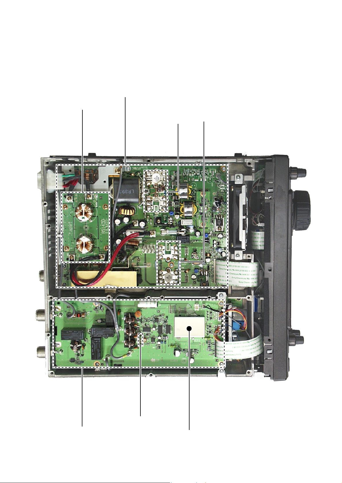
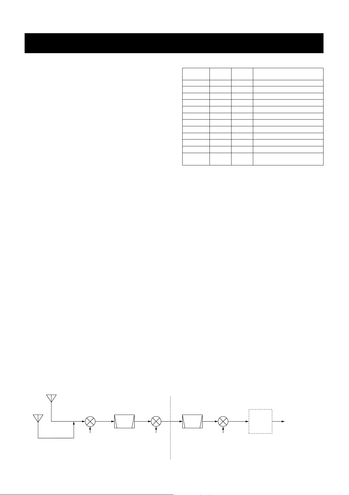
4-1-4 1ST MIXER AND 1ST IF CIRCUITS (RF UNIT)
The 1st mixer circuit mixes the received signals with the 1st
LO signal to convert the received signals into a fixed 64.455
MHz 1st IF signal.
The signals from the pre-amplifier circuit, or signals which
bypass the pre-amplifier circuit, are applied to the 1st mixer
(Q211, Q212) and mixed with the 1st LO signal (64.485–
238.455 MHz) coming from the 1st LO PLL circuit via the LO
amplifier (Q301) and low-pass filter.
The mixed 1st IF signal is passed through the MCFs (Mono-
lithic Crystal Filter: FI231a/b) to suppress out-of-band sig-
nals. The filtered signal is amplified at the IF amplifier (Q241),
and then applied to the 2nd mixer circuit.
When the bandscope function is activated, the 1st LO
sweeping signal is supplied to the 1st mixer circuit.
4-1-5 2ND MIXER CIRCUIT (RF UNIT)
The 2nd mixer circuit converts the 1st IF signal into the 2nd
IF frequency by mixing with the 2nd LO signal (64.00 MHz).
The 1st IF signal from the IF amplifier (Q241) is applied and
converted into a 455 kHz 2nd IF signal at the 2nd mixer cir-
cuit (D261) by mixing with a fixed 64 MHz 2nd LO signal.
The 2nd IF signal is passed through the low-pass filter (L263,
C262–C264) to suppress undesired signals such as the 2nd
LO signal, and the applied to the MAIN unit via J261.
The 2nd LO signal is a doubled reference frequency, gener-
ated at the reference oscillator (X1901: 32.0 MHz) and dou-
bled at Q1903 and Q1904.
4-1-6 NOISE BLANKER CIRCUIT (MAIN UNIT)
The noise blanker circuit detects pulse-type noise, and turns
OFF the signal line when the noise appears.
The 2nd IF signal from the RF unit is applied to the noise
blanker gate (D252, D253). A portion of the 2nd IF signal
from RF unit is amplified at the noise amplifiers
(Q200–Q203), and is then detected at the noise detector
(D200) to convert the noise components to DC voltages.
The signal is then applied to the noise blanker switch (Q206,
Q207). At the moment detected voltage exceeds Q206’s
threshold level, Q207 outputs a blanking signal to close the
noise blanker gate (D252, D253). The PLL unlock signal are
also applied to Q207 to control the noise blanker gate.
Some DC voltage from the noise detector circuit is fed back
to the noise amplifiers (Q200, Q201) via the DC amplifiers
(Q204, Q205). The DC amplifiers function as an AGC circuit
to reduce average noise. Therefore, the noise blanker func-
tion shuts off pulse-type noise only.
4-1-7 2ND IF CIRCUIT (MAIN UNIT)
The 2nd IF circuit amplifies and filters the 2nd IF signal, and
applies the 2nd IF signal to the 3rd mixer circuit.
The 2nd IF signal from the noise blanker gate (D252, D253)
is amplified at the 2nd IF amplifier (Q250) and passed
through the ceramic filters (FI271, FI272). The filtered signal
is applied to the 3rd mixer circuit.
4-1-8 3RD MIXER AND 3RD IF CIRCUITS
(MAIN UNIT)
The 3rd mixer circuit mixes the 2nd IF signal with the 3rd LO
signal to obtain the 3rd IF (36 kHz) signal.
The 2nd IF signal from the ceramic filters (FI271, FI272) is
applied to the 3rd mixer circuit (IC280, pin 1). The 3rd LO
signal from the 3rd LO PLL circuit is also applied to the 3rd
mixer (IC280, pin 5). The mixed signal is output from pin 6.
The 3rd IF signal is passed through the low-pass filter
(IC1460a) and amplified at the 3rd IF amplifier (IC1460b).
The filtered and amplified signal is then applied to the DSP
unit via DRIF line.
4-1-9 DSP RECEIVER CIRCUIT (DSP UNIT)
The DSP (Digital Signal Processor) circuit enables digital IF
filter, digital noise reduction, PSN (Phase Shift Network)/
Low Power/Phase demodulation, digital automatic notch,
and etc.
The 36 kHz 3rd IF signal from the 3rd IF amplifier (MAIN
unit; IC1460b) is amplified at the differential amplifiers
(IC651a/b), and is then applied to the A/D converter section
in the CODEC IC (IC501). At the same time, the converted
signal is level-shifted 5V to 3.3 V in the IC (IC501).
The level-shifted signal is applied to the DSP IC (IC301) for
the digital IF filter, demodulator, automatic notch and noise
reduction, etc.
The output signal from the DSP IC is applied to the D/A con-
verter section in the CODEC IC (IC501) to convert into the
analog audio signals. Also the signals are level-shifted 3.3 V
to 5V at the level converter section in the IC (IC501).
The level-shifted audio signals are passed through the
active filter (IC701a), and then applied to the MAIN unit via
J901 (pin 17) as the DRAF signal.
Differential
converter
DRIF DRAF
•DSP receiver circuit
IC651b/a
DSP IC
IC301
Aactive
filter
IC701a
A/D
converter
Level
converter
Level
converter
D/A
converter
IC501 CODEC IC
MAIN unit DSP unit MAIN unit
36 kHz
3rd IF
signal
AF
signals
for
free
by
RadioAmateur.eu

4 - 3
4-1-10 TWIN PBT CIRCUIT (DSP UNIT)
General PBT (Passband Tuning) circuit shifts the center fre-
quency of IF signal to electronically narrow the passband
width. The IC-746PRO/7400 uses the DSP circuit for the
digital PBT function and actually shifts the both lower and
higher passbands of 3rd IF filter within ±1.8 kHz.
The twin PBT circuit in DSP IC (IC301) controlled by the
[TWIN PBT] controller adjusts the 3rd IF passband width
and rejects interference.
4-1-11 AGC CIRCUIT (DSP UNIT)
The AGC (Automatic Gain Control) circuit reduces IF ampli-
fier gain and attenuates IF signal to keep the audio output at
a constant level.
The receiver gain is determined by the voltage on the AGC
line (MAIN unit; IC1401, pin 14). The D/A converter for AGC
(IC102) supplies control voltage to the AGC line and sets the
receiver gain with the [RF/SQL] control.
The 3rd IF signal from the CODEC IC (IC501) is detected at
the AGC detector section in the DSP IC (IC301). The output
signal from the DSP IC (IC301) is level-shifted at the level
converter (IC101) and applied to the D/A converter (IC102).
The AGC voltage is amplified at the buffer amplifier section
in IC102 and is applied to the MAIN unit to control the AGC
line.
When receiving strong signals, the detected voltage increas-
es and the AGC voltage decreases via the buffer amplifier
(IC102). As the AGC voltage is used for the bias voltage of
the IF amplifiers (RF unit; Q241, MAIN unit; Q250), IF ampli-
fier gain is decreased.
4-1-12 SQUELCH CIRCUIT (MAIN UNIT)
The squelch circuit mutes audio output when the S-meter
signal is lower than the [RF/SQL] setting level.
The NSQL or VSQL signal from the DSP unit is applied to
the main CPU (IC1500) and is compared with the threshold
level set by the [RF/SQL] control. The [RF/SQL] setting sig-
nal is passed through the sub CPU (DISPLAY board;
IC1001, pin 91), and then applied to the main CPU. The
main CPU analyzes the compared signal and outputs con-
trol signal to the squelch gate (IC1160, pin 5) to open or
close the squelch as the SQLS signal.
4-1-13 AF AMPLIFIER CIRCUIT (MAIN UNIT)
The AF amplifier amplifies the audio signals to a suitable dri-
ving level for the speaker.
The AF signals (DRAF) from the DSP unit are passed
through the squelch gate (IC1160) and amplified at the AF
amplifier section of IC1180 (pins 2, 4), and volume is con-
trolled by the AFGV signal at the VCA section (pins 7–9).
The volume controlled AF signals are passed through the AF
mute gate (IC1220, pins 7, 1), then applied to the AF power
amplifier (IC1240, pin 1) via the ripple filter (Q1280).
The amplified audio signals are passed through the
[PHONES] and [EXT SP] jacks then applied to the internal
speaker when no plug is connected to the jacks.
The AF mute gate is controlled by the [AF] control via the
sub and main CPUs.
4-1-14 TONE SQUELCH CIRCUIT (MAIN UNIT)
A portion of the detected FM audio signals from the DSP unit
via the MONI line are amplified at the AF amplifier (IC1060).
The amplified signals are applied to the low-pass filter
(IC1001) to cut-out the 300 Hz or higher audio components,
and subaudible tone signals only pass through. The filtered
signal (subaudible tone) is then applied to the main CPU
(IC1500, pin 108).
The main CPU detects the frequency of the applied subaudi-
ble tone signal and releases the audio mute when a matched
tone frequency signal is detected.
[PHONES]
[EXT SP]
Int. speaker
IC1240
AF
power
amp.
DRAF
•AF amplifier circuit
7
6
1
IC1160 IC1180
Mute switchSquelch gate
Ripple
filter
Q1260
MAIN unitDSP unit
“SQLS”signal
“AFGV”signal
56
7
1
IC1120
“AFMS”signal
5
AMP VCA
for
free
by
RadioAmateur.eu

4 - 4
4-2 TRANSMITTER CIRCUITS
4-2-1 MICROPHONE AMPLIFIER CIRCUIT
(MAIN UNIT)
The microphone amplifier circuit amplifies microphone audio
signals to a level needed for the DSP circuit.
Audio signals from the [MIC] connector (MIC board; J1, pin
1) are amplified at the audio amplifier section in IC1400
(pins 2, 4), and then applied to the VCA section (IC1400, pin
7). The gain controlled signals are output from (IC1400, pin
9) and amplified at the AF amplifier (IC1401, pins 1–3) and
passed through the low-pass filters (IC1401, pins 5–9) and
analog switch (IC1310, pins 12, 14). The signals are then
applied to the DSP circuit as the DTAF signal.
The VCA section in IC1400 (pins 7–9) controls microphone
input gain according to the [MIC GAIN] control level using
the MIGV signal coming from the main CPU via the I/O
expander (IC502, pin 3).
4-2-2 VOX CIRCUIT (MAIN UNIT)
The VOX (Voice-Operated-Transmission) circuit sets trans-
mitting conditions according to voice input.
When the VOX function is activated, a portion of the micro-
phone signals are amplified at the VOX amplifier (IC1280
pins 3, 1) and applied to main CPU (IC1500, pin 109) via the
VOXL line. A portion of the power amplified AF signals from
the AF power amplifier (IC1240) are amplified at the anti-
VOX amplifier (IC1121, pins 6, 7) and applied to the main
CPU (IC1500, pin 110) via the AVXL line. Then the main CPU
compares these and controls the transmitter circuit.
4-2-3 DSP TRANSMITTER CIRCUIT (DSP UNIT)
The DSP (Digital Signal Processor) circuit enables PSN
(Phase Shift Network)/Low Power/Phase modulation, trans-
mitter monitor, side tone, and etc.
The microphone audio signals from the MAIN unit via the
DTAF line are amplified at the differential amplifiers
(IC601a/b), and are then applied to the A/D converter sec-
tion in the CODEC IC (IC501). At the same time, the con-
verted signals are level-shifted 5 V to 3.3 V in the IC (IC501).
The level-shifted signal are applied to the DSP IC (IC301)
and modulated at the DSP IC to produce the 36 kHz trans-
mitter IF signal.
The modulated IF signal from the DSP IC is applied to the
D/A converter section in the CODEC IC (IC501) to convert
into the analog IF signal. Also the signal is level-shifted 3.3
V to 5V at the level converter section in the IC (IC501).
The level-shifted IF signal is passed through the active filter
(IC701b), and then applied to the MAIN unit via J901 (pin
22) as the DTIF signal.
4-2-4 SPEECH COMPRESSOR CIRCUIT
(DSP UNIT)
The speech compressor compresses the transmitter audio
input signals to increase the average output level (average
talk power).
When the speech compressor function is ON, the level-shift-
ed signal from the CODEC IC (IC501) is applied to the DSP
IC (IC301) and compressed at the DSP IC to obtain an aver-
age audio level.
At the same time, the compressed signals are modulated at
the DSP IC and applied to the D/A converter section in the
CODEC IC (IC501).
4-2-5 IF AMPLIFIER AND MIXER CIRCUITS
(MAIN AND RF UNITS)
The modulated 3rd IF signal from the DSP unit (DTIF: 36
kHz) is amplified at the 3rd IF amplifier (MAIN unit; IC1120a)
and passed through the low-pass filters (MAIN unit;
IC1120b/c). The filtered signal is applied to the 3rd mixer cir-
cuit (MAIN unit; IC400, pin 1). The applied 3rd IF signal is
mixed with the 3rd LO signal from the DDS circuit (RF unit;
IC1601) to produce a 455 kHz 2nd IF signal.
The 2nd IF signal is output from pin 6 and passed through
the ceramic bandpass filter (MAIN unit; FI381) for unwanted
signals are suppressed. The filtered 2nd IF signal is ampli-
fied at the 2nd IF amplifier (MAIN unit; Q330). The amplified
signal is applied to the 2nd mixer circuit on the RF unit via
J250.
The 2nd IF signal is mixed with the 64 MHz 2nd LO signal,
coming from the PLL circuit, at the 2nd mixer circuit (RF unit;
D261) to obtain a 64.455 MHz 1st IF signal. The 1st IF sig-
nal is passed through the MCFs (RF unit; FI231b/a) to cut-
off the undesired signals, and is then amplified at the 1st IF
amplifier (RF unit; Q271) via the T/R switch (RF unit; D251).
The amplified 1st IF signal is applied to the 1st IF mixer cir-
cuit (RF unit; D271) via the attenuator (RF unit; D272) and
low-pass filter circuit.
•Transmitter construction
1st LO
D271
Ceramic
filter
Crystal
filter
FI231b/a
LPF BPFs
FI381
MIC
Bandwidth
15 kHz
455 kHz
DSP
unit
RF UNIT
MAIN UNIT
AMP VCA 3rd LO
(491 kHz)
IC400
64.455 kHz
2nd LO
(64.00 MHz)
D261
36 kHz IF
IC1400
9
13
14
12
IC1310
“MODS”signal
DTAF DTIF
for
free
by
RadioAmateur.eu

4 - 5
The operating (transmitting) frequency is produced at the 1st
IF mixer circuit (RF unit; D271) by mixing the 1st IF and 1st
LO signals. The mixed signal is then applied to the RF cir-
cuit.
4-2-6 RF CIRCUIT (RF AND PA UNITS)
The RF circuit amplifies operating (transmitting) frequency
to obtain 100 W of RF output.
The signal from the 1st IF mixer is passed through one of the
low-pass or bndpass filters (Refer to page 4-1 for bandpass
filters used) and high-pass filters after passing through the
low-pass filter (RF unit; L285, L286, C286–C289, C291).
The filtered RF signal is amplified at the wide-band YGR
amplifier (RF unit; IC151), and is then applied to the PA unit
via J151.
The signal applied from the RF unit is amplified at the 2 pre-
drive (PA unit; Q1, Q2) and drive (DRV board; Q1, Q2) am-
plifiers. These amplifiers cover all HF, 50 MHz and 144 MHz
band amplifying operation.
When operating on the HF or 50 MHz band, the signal from
the drive amplifier is power amplified at the HF/50 MHz
power amplifier (PA unit; Q5, Q6) via the band switching relay
(PA unit; RL2). However, the 144 MHz signal is power am-
plified at the 144 MHz power amplifier (PA unit; Q201, Q202)
to obtain a stable 100 W of RF output power.
The amplified signal is applied to the desired antenna con-
nector via one of 8 low-pass filters.
4-2-7 ALC CIRCUIT (MAIN UNIT)
The ALC (Automatic Level Control) circuit controls the gain of
IF amplifiers in order for the transceiver to output a constant
RF power set by the [RF PWR] control even when the sup-
plied voltage shifts, etc.
The RF power level is detected at the SWR detector circuit
(HF/50 MHz bands: CTRL unit; D2, 144 MHz band: PA unit;
D602) to be converted into DC voltage and applied to the
MAIN unit as the FOR (HF/50 MHz) or VFOR (144 MHz) sig-
nal.
The FOR or VFOR signal is applied to the comparator
(IC300, pin 6). The POCV signal, controlled by the [RF PWR]
control via the I/O expander (IC502, pin 4), is also applied to
the other input (pin 5) for reference. The compared signal is
output from pin 7 and applied to the IF amplifiers in the MAIN
(Q330) and RF (Q271) units to control amplifying gain.
When the FOR or VFOR signal exceeds the POCV voltage,
ALC bias voltage from the comparator controls the IF ampli-
fiers. This adjusts the output power to a specified level from
the [RF PWR] control until the FOR (VFOR) and POCV volt-
ages are equalized.
In AM mode, the comparator operates as an averaging ALC
amplifier. Q304 turns ON and the POCV voltage is shifted for
40 W AM output power (maximum) through R320.
The ALC bias voltage is also applied to the ALC meter am-
plifier (IC300, pin 2) to obtain an ALC meter signal (ALCL).
The amplified signal is passed through the analog switch (IC
1900, pins 5, 4) and applied to the main CPU (IC1500, pin
107) to drive the S/RF meter via the sub CPU (IC1001) on
the DISPLAY board.
An external ALC input from the [ALC] jack or [ACC] sockets
is applied to the buffer amplifier (Q307). External ALC oper-
ation is identical to that of the internal ALC.
The FOR or VFOR signal is also applied to the power meter
amplifier (IC360, pin 3). The amplified signal is applied to the
main CPU (IC1500) after being switched by the analog
switch (IC1900, pins 12, 14) as an FORL signal to drive the
S/RF meter via the sub CPU (DISPALY board; IC1001).
4-2-8 APC CIRCUIT (MAIN UNIT)
The APC (Automatic Power Control) circuit protects the
power amplifiers on the PA unit from high SWR and exces-
sive current.
The reflected wave signal appears and increases when the
connected antenna is mismatched to 50 Ω. The SWR detec-
tor circuit (HF/50 MHz bands; CTRL unit; D1, 144 MHz band;
PA unit; D603) detects the reflected signal, and applies it to
the APC circuit (IC300, pin 9) as a REF (HF/50 MHz) or
VREF (144 MHz) signal.
When the REF or VREF signal level increases, the APC cir-
cuit decreases the ALC voltage to activate the APC.
For the current APC, the power transistor current is obtained
by detecting the voltages (ICH and ICL) which appear at both
terminals of the current detector (PA unit; R28). The detected
voltages are applied to the differential amplifier (IC300, pins
12, 13). When the current of transistors is increased, the am-
plifier controls the ALC line to prevent excessive current flow.
A portion of the REF or VREF signal is applied to the SWR
meter amplifier (IC360, pin 5). The amplified signal is applied
to the main CPU (IC1500) after being switched by the analog
switch (IC1900, pins 2, 15) as an REFL signal to drive the
SWR meter.
Differential
converter
DTAF DTIF
•DSP receiver circuit
IC601b/a
DSP IC
IC301
Aactive
filter
IC701b
A/D
converter
Level
converter
Level
converter
D/A
converter
IC501 CODEC IC
MAIN unit DSP unit MAIN unit
AF
signal 36 kHz
IF signal
for
free
by
RadioAmateur.eu

4 - 6
4-2-9 TEMPERATURE PROTECTION CIRCUIT
(MAIN AND RF UNITS)
The cooling fan (CHASSIS; MF1) is activated while transmit-
ting or when the temperature of the power amplifier exceeds
the preset value. The temperature protection circuit consists
of Q801, Q802 and D802 (MAIN unit), IC1101 and
Q2003–Q2005 (RF unit), and VARISTOR-A/B/C/D boards.
While transmitting, IC1101 (RF unit) outputs FANL signal to
Q2003 (RF unit). Then Q2003 (RF unit) is turned ON, Q801,
Q802 (MAIN unit) provide a voltage to the cooling fan to ro-
tate at low speed. The VARISTOR-B board, detects the tem-
perature of Q6; PA unit (VARISTOR-D board for Q202; PA
unit), and IC1101 (RF unit) outputs FANM signal and acti-
vates Q2004 (RF unit) to accelerate the cooling fan at
medium speed when the detected temperature exceeds
70˚C (158˚F). When the detected temperature is at 80˚C
(176˚F) or more, IC1101 (RF unit) outputs FANH signal and
activates Q20065 (RF unit), the cooling fan rotates at high
speed.
The temperature protection circuit keeps the cooling fan ro-
tating even while receiving until the Q6 (PA unit) or Q202’s
(PA unit) temperature drops to 60˚C (140˚F) or below.
4-2-10 MONITOR CIRCUIT
(DSP UNIT AND MAIN UNIT)
The microphone audio signals can be monitored to check
voice characteristics.
(1) When FM/AM modes (MAIN UNIT)
A portion of the microphone audio signals are passed
through the DSP unit, and then applied to the AF amplifier
circuit as the MONI signal.
(2) When SSB/RTTY modes (DSP UNIT)
A portion of the transmit IF signal from the DSP IC (IC301)
is mixed with a 36 kHz LO signal to demodulate into the AF
signals. The demodulated signals are level-shifted 3.3 V to
5 V at the level converter (IC101) and then applied to the
D/A converter (IC102) to convert into the analog AF signal.
The AF signals are then applied to the MAIN unit as the
MONI signal.
The MONI signal from the DSP unit is amplified at the AF
amplifier (MAIN unit; IC1060, pins 5, 7) and passed through
the analog switch (MAIN unit; IC1040) and then applied to
IC1180 (MAIN unit). The applied signal is amplified at the AF
amplifier section (pins 2, 4) and volume controlled at the
VCA section (pins 7, 9). The volume controlled AF signals is
applied to the AF amplifier circuit (MAIN unit; IC1240).
4-3 PLL CIRCUITS
4-3-1 GENERAL
The PLL circuits generate a reference frequency (32.000
MHz); 1st LO frequencies (64.485–238.455 MHz); 2nd LO
frequency (64 MHz), 3rd LO frequency (419.000 kHz).
The 1st LO PLL adopts a mixer-less dual loop PLL system
and has 4 VCO circuits which cover from 30 kHz to 174 MHz.
The 1st LO and 3rd LO use DDSs, while the 2nd LO uses
the fixed frequency of the crystal oscillator.
4-3-2 1ST LO PLL CIRCUIT (RF UNIT)
The 1st LO PLL contains a main and reference loop as a
dual loop system.
The reference loop generates an approximate 10.8 MHz fre-
quency using a DDS circuit, and the main loop generates a
64.485 to 238.455 MHz frequency using the reference loop
frequency.
(1) REFERENCE LOOP PLL
The oscillated signal at the reference VCO (Q1301, D1301)
is amplified at the amplifiers (Q1302, Q1102) and is then ap-
plied to the DDS IC (IC1101, pin 46). The signal is then di-
vided and detected on phase with the DDS generated
frequency.
The detected signal output from the DDS IC (pin 56) is con-
verted into DC voltage (lock voltage) at the loop filter (R1135,
R1138, C1121) and then fed back to the reference VCO cir-
cuit (Q1301, D1301).
(2) MAIN LOOP PLL
The oscillated signal at one of the main loop VCOs (VCO
board, Q1201, D1201, Q1221, D1221, Q1241, D1241,
Q1261, D1261) is amplified at the buffer amplifiers (PLL
board, IC1802, Q1281) and is then applied to the PLL IC
(IC1801, pin 4). The signal is then divided and detected on
phase with the reference loop output frequency.
The detected signal output from the PLL IC (pin 13) is con-
verted into a DC voltage (lock voltage) at the loop filter and
then fed back to one of the VCO circuits (VCO board, Q1201,
D1201, Q1221, D1221, Q1241, D1241, Q1261, D1261).
The oscillated signal from the buffer amplifier (IC1802) is also
applied to the MAIN unit as a 1st LO signal after being dou-
bled or passed through the low-pass filter.
•Using VCO and 1st LO frequencies
4-3-3 2ND LO AND REFERENCE OSCILLATOR
CIRCUITS (RF UNIT)
The reference oscillator (X1901, Q1901) generates a 32.0
MHz frequency for the 2 DDS circuits as a system clock and
for the LO output. The oscillated signal is doubled at the dou-
bler circuit (Q1903, Q1904) and the 64.0 MHz frequency is
picked up at the double tuned filter (L1903, L1904). The 64.0
MHz signal is applied to the RF circuit as a 2nd LO signal.
Operating Using VCO 1st LO frequency
frequency
0.03–Q1201, D1201 64.4850–72.454999 MHz
7.999999 MHz
8.0–Q1221, D1221 72.4550–86.454999 MHz
21.999999 MHz
22.0–Q1241, D1241 86.4550–104.454999 MHz
39.999999 MHz
40.0–Q1261, D1261
104.4550–124.455000 MHz
60.000000 MHz
108.0–Q1241, D1241
172.4550–208.454999 MHz
143.999999 MHz (with doubler)
144.0–Q1261, D1261
208.4550–238.455000 MHz
174.000000 MHz (with doubler)
for
free
by
RadioAmateur.eu

4 - 7
4-3-4 3RD LO CIRCUIT (RF UNIT)
The DDS IC (IC1601) generates a 10-bit digital signal using
the 32 MHz system clock. The digital signal is converted into
an analog wave signal at the D/A converter (R1601–R1620).
The converted analog wave is passed through the bandpass
filter (L1602, L1603, L1605, C1609–C1613, C1615–C1617)
and then applied to the MAIN unit as the 3rd LO signal
(491.000 kHz).
4-3-5 MARKER CIRCUIT (RF UNIT)
The divided signal at the DDS circuit (IC1101) is used for the
marker signals with the IC-746PRO/7400.
The reference signal for the DDS circuit (32.0 MHz) is di-
vided by 2 to produce an acceptable frequency signal, 16
MHz, with the programmable divider then divided again by
160 to obtain 100 kHz cycle square-wave signals.
The generated marker signals are output from pin 49 of the
DDS IC (IC1101) and then applied to the 1st mixer circuit
(Q211, Q212) via the marker switch (IC1081) as the MKR
signal.
4-4 ANTENNA TUNER CIRCUITS
4-4-1 MATCHING CIRCUIT (TUNER UNIT)
The matching circuit is a T-network. Using 2 tuning motors,
the matching circuit obtains rapid overall tuning speed.
Using relays (RL1–RL15), the relay control signals from the
antenna tuner CPU (CTRL unit; IC5) via the buffer amplifier
(Q1–Q15) ground one of the taps of L3–L9, L11, L12 and
add capacitors (C34–C43). After selecting the coils and ca-
pacitors, 2 motors (MF1, MF2) adjust C44 and C45 using the
antenna tuner CPU (CTRL unit; IC5) and the motor driver cir-
cuit (CTRL unit; Q211–Q218) to obtain a low SWR (Stand-
ing Wave Ratio).
4-4-2 DETECTOR CIRCUITS (CTRL UNIT)
(1) SWR detector
Forward and reflected power are picked up by a current
transformer (L1), detected by D1 and D2, and then amplified
at IC1b and IC1a, respectively. The amplified voltages are
applied to the antenna tuner CPU (IC5, pins 2, 3). The an-
tenna tuner CPU detects the SWR.
(2) Reactance components detector
Reactance components are picked up by comparing the
phases of the RF current and RF voltage. The RF current is
detected by L4 and R16, and rectified at D5. The rectified
current is amplified at the C-MOS inverter amplifier (IC14e)
and buffer amplifier (IC2a). The amplified signal is then ap-
plied to the phase comparator (IC3a).RF voltage is detected
by C12–C14 and rectified at D4. The rectified voltage is am-
plified at the C-MOS inverter amplifier (IC14c) and buffer am-
plifer (IC2b). The amplified signal is then applied to the phase
comparator (IC3b).
The output signal from the phase comparator (IC3a, pin 6 for
RF current, IC3b pin 7 for RF voltage) is rectified at D7 and
D6 for conversion into DC voltage. The rectified voltages are
combined, and amplified at IC4b, then applied to the antenna
tuner CPU (IC5, pin 64).
A C-MOS inverter IC is used for the buffer-amplifier (IC14) to
improve functionable sensitivity. The C-MOS inverter ampli-
fier is very responsive, and ensure quick and stable signal
detection, even at a low RF signal level input.
(3) Resistance components detector
Resistance components are picked up by L8, and detected
by D8, D9 and Q5. The detected resistance components are
amplified at the amplifier (IC4a), and then applied to the an-
tenna tuner CPU (IC5, pin 1).
4-4-3 MOTOR CONTROL CIRCUIT
The control circuit of the internal antenna tuner consists of
the CPU, EEPROM*, tuning motors and tuning relays.
*Electronically-Erasable Programmable Read Only Memory
•PLL circuit
64.485–238.455 MHz
64.0 MHz
1st mixer
Q211, Q212
491 kHz
IC1601
IC1101
IC1801
Q1903
Q1904
RF unit MAIN unit
Q1201
Q1221
Q1241
Q1261
Q1301
1st LO PLL circuit
Phase
detector
1/N divider Phase
detector
12 bit
D/A
Main loop PLL
Ref. loop PLL
DDS
×2
DDS
D/A
Crystal
filter
2nd mixer
D261
3rd mixer
IC631
64.455 MHz
to DSC unit
Reference oscillator
X1901: 32.0 MHz
BPFBPF
×2
or
×1
RF signal
ANT
1/22
for
free
by
RadioAmateur.eu

4 - 8
(1) CPU and EEPROM (CTRL unit)
The antenna tuner CPU (IC5) controls the tuning motors via
the motor driver circuit (Q211–Q218) and tuning relays di-
rectly, and memorizes the best preset position in 100 kHz
steps. The memory contents are stored in the EEPROM
(IC6) without a backup battery.
(2) Tuning motors (CTRL unit)
The motor driver circuit (Q211–Q218) rotates the tuning mo-
tors (MF1, MF2) to obtain a low SWR.
(3) Tuning relays (TUNER unit)
According to the operating frequency band and antenna con-
dition, tuning relays select the capacitors (C34–C43) and
coils ( L3–L9, L11, L12).
4-5 POWER SUPPLY CIRCUITS
4-5-1 PA UNIT
4-5-2 S-LOGIC BOARD
4-5-3 MAIN UNIT
4-5-4 PLL UNIT
4-4-4 ANTENNA TUNER CPU PORT ALLOCATION
(CTRL unit; IC5)
1
2
3
4
7
13
15
17
19
21
22, 23
25,
34–36
38–40
26–32
41–44
45–48
64
Input port for the resistance com-
ponents detection voltage.
Input port for the reflected RF
power voltage.
Inpout port for the forward RF
power voltage.
Input port for the transceiver power
OFF.
Input port for the reference voltage
setting.
Outputs tuner data signal.
Input port for the serial signal.
Outputs the [TUNER] ON/OFF sig-
nal.
Input port for reset signal.
Input port for the TX/RX switching
signal.
Input ports for the antenna tunner
CPU system clock.
Output the capacitor selection sig-
nals.
Output the coil selection signals.
Output ports for the tuning motor
(MF2) drive signals.
Output ports for the tuning motor
(MF1) drive signals.
Input port for the reactance compo-
nents detection voltage.
AN2
AN1
AN0
PWRS
SETI
CIKY
CIST
THRU
CDRS
TRC
XIN, XOUT
NVHF, CO3,
CO2, CO1,
CI3, CI2, CI1
VHF, 24M,
18M, 14M,
10M, 7M, 4M
P07–P04
P03–P00
AN3
Pin Port Description
number name
Line Description
–8 V Common –8 V converted from the 14V line and
regulated by the –8 V DC-DC converter (IC401).
Line Description
H14V The voltage from an external power supply via
the common filter circuit (FILTER board, L1).
HV The same voltage as the H14V line passed
through a fuse.
14VS The same voltage as the HV line passed through
the switching relay (RL1).
14V The same voltage as the 14VS line passed
through coils (L22, L23).
8V Common 8 V converted from the 14V line and
regulated by the +8 regulator circuit (IC3).
5V Common 5 V converted from the 14V line and
regulated by the +5 regulator circuit (IC2).
H5V Common 5 V converted from the HV line and
regulated by the +5 regulator circuit (IC1).
Line Description
R8V
Receive 8 V converted from the 14V line and
regulated by the R8V regulator circuit (Q451,
Q453).
T8V
Transmit 8 V converted from the 14V line and
regulated by the T8V regulator circuit (Q450,
Q452).
Line Description
5VPLL Common 5 V converted from the 8V line and
regulated by the 5 V regulator circuit (IC1051).
for
free
by
RadioAmateur.eu

5 - 1
SECTION 5 ADJUSTMENT PROCEDURES
5-1 PREPARATION BEFORE SERVICING
■REQUIRED TEST EQUIPMENT
DC power supply
RF power meter
(terminated type)
Frequency counter
RF voltmeter
FM deviation meter
Modulation analyzer
Distortion meter
Oscilloscope
Audio generator
Standard signal
generator (SSG)
Digital multimeter
AC millivoltmeter
DC voltmeter
DC ammeter
Spectrum analyzer
Attenuator
External speaker
Terminator
EQUIPMENT GREDE AND RANGE EQUIPMENT GREDE AND RENGE
Output voltage : 13.8 V DC
Current capacity : 30 A or more
Measuring range : 10–200 W
Frequency range : 1.8–200 MHz
Impedance : 50 Ω
SWR : Less than 1.2 : 1
Frequency range : 0.1–200 MHz
Frequency accuracy : ±1 ppm or better
Sensitivity : 100 mV or better
Frequency range : 0.1–200 MHz
Measuring range : 0.01–10 V
Frequency range : DC–200 MHz
Measuring range : 0 to ±5 kHz
Frequency range : At least 200 MHz
Measuring range : 0–100 %
Frequency range : 1 kHz ±10 %
Measuring range : 1–100 %
Frequency range : DC–20 MHz
Measuring range : 0.01–20 V
Frequency range : 300–3000 Hz
Measuring range : 1–500 mV
Frequency range : 0.1–200 MHz
Output level : 0.1 µV to 32 mV
(–127 to –17 dBm)
Imput impeadance : 10 MΩ/DC or beter
Measuring range : 10 mV–10 V
Input impedance :
50 kΩ/V DC or better
Measurement capability: 1 A/30 A
Frequency range : At least 90 MHz
Spectraum bandwidth : 100 kHz or more
Power attenuation : 50 or 60 dB
Capacity : 150 W or more
Input impedance : 8 Ω
Capacity : 5 W or more
Resistance :
50 Ωand 100 or 25 Ω
Capacity : 150 W or more
‘‘CONNECTIONS
[ANT1] [ANT2] [ANT 144MHz]
FM deviation meter
Modulation analyzer
RF power meter
Spectrum analyzer
Attenuator
Distortion meter
DC power supplyAmmeter
Standard signal
generator
CAUTION !
DO NOT transmit while
an SSG is connected to
the antenna connector.
to the antenna connector
to [DC 13.8 V]
to [SP]
Speaker
Audio generator
PTT
+–
[MIC]
Terminator
2-conductor 3.5 (d) mm (1⁄8")
Shorten inner and outer terminals.
For entering the “ADJUSTMENT
MODE”, connected to [REMOTE].
for
free
by
RadioAmateur.eu

5 - 2
5-2 PLL ADJUSTMENTS
REFERENCE
FREQUENCY
LPL LOCK
VOLTAGE
VCO LOCK
VOLTAGE
1LO
OUTPUT
LEVEL
3LO
OUTPUT
LEVEL
MARKER
OUTPUT
LEVEL
ADJUSTMENT
ADJUSTMENT ADJUSTMENT CONDITION MEASUREMENT VALUE POINT
UNIT LOCATION UNIT ADJUST
1
2
1
1
2
3
4
1
1
1
•Displayed freq. : Any
•Preset R1032 (RF unit) to the cen-
ter position.
•Preset L1902 (RF unit) approxi-
mate 1.5 mm downside from top of
the coil’s case.
•Receiving
•Receiving
•Displayed freq. : 0.030000 MHz
•Mode : USB
•Receiving
•Displayed freq.
: 7.999999 MHz
•Mode : USB
•Receiving
•Displayed freq.
: 21.999999 MHz
•Mode : USB
•Receiving
•Displayed freq.
: 39.999999 MHz
•Mode : USB
•Receiving
•Displayed freq.
: 60.000000 MHz
•Mode : USB
•Receiving
•Displayed freq.
:
0.500000 MHz, 7.999999 MHz
8.000000 MHz, 21.999999 MHz
22.000000 MHz, 39.999999 MHz
40.000000 MHz, 50.000000 MHz
54.000000 MHz, 144.000000 MHz,
148.000000 MHz
•Receiving
•Displayed freq.
: Any
•Mode : USB
•Receiving
•Displayed freq.
: 14.100000 MHz
•Mode : CW
•Marker : ON
•Receiving
RF
RF
RF
RF
RF
FRONT
Connect an RF volt-
meter to the check
point P1901.
Connect a frequency
counter to the check
point P1901.
Connect a digital
multimeter or oscillo-
scope to the check
point CP1101 (LV1).
Connect a digital
multimeter or oscillo-
scope to the check
point CP1801 (LV2).
Connect an RF volt-
meter to the check
point CP1500.
Connect an RF volt-
meter to the check
point CP1601.
Display
Maximum level
(0 dB or more)
64.000000 MHz
1.0 V
4.0 V
–7 dBm or more
–25 dBm or more
S3 or more
(S-meter level)
RF
RF
RF
L1903,
L1904,
L1901
(L1902, R1032
for critical
adjustment)
C1303
C1208
C1228
C1248
C1268
Verify
Verify
Verify
for
free
by
RadioAmateur.eu

5 - 3
R1032
Reference frequency
adjustment
Reference
frequency
adjustment
VCO lock
voltage
adjustment
L1904
L1901
L1902
L1903
P1901
Reference frequency
check point
CP1101 (LV1)
LPL lock voltage
check point
C1303
LPL lock voltage
adjustment
C1208
C1228
C1248
C1268
CP1801 (LV2)
VCO lock voltage
check point
CP1601
3rd LO output level
check point
CP1500
1st LO outoput level
check point
for
free
by
RadioAmateur.eu

5-3 TRANSMITTER ADJUSTMENTS
IDLING
CURRENT
(for driver)
(for HF/50 M
band final
amplifier)
(for 144 M
band final
amplifier)
144 M PEAK
TX PEAK
TRANSMITTER
TOTAL GAIN
Ic APC
1
2
3
1
1
2
3
1
1
•Displayed freq. : 14.100000 MHz
•Mode : USB
•[MIC GAIN] : Max.CCW
•[RF POWER] : Max. CW
•[TUNER] : OFF
•Preset R11, R18, R204 (PA unit) to
max. counter clockwise.
•Turn C202 (PA unit) to 90˚clock-
wise.
•Transmitting
•Transmitting
•Displayed freq. : 144.00000 MHz
•Mode : USB
•Transmitting
•Displayed freq. :
146.00000 MHz [USA]
144.00000 MHz [except USA]
•Mode : RTTY
•Transmitting
•Displayed freq. : 145.00000 MHz
•Mode : USB
•Set following controls as:
[RF POWER] : Max. CW
[MIC GAIN] : Center
[KEY SPEED]: Center
[PITCH] : Center
•Disconnect P1 (PA unit) from J151
(RF unit).
•Connect an audio generator to
[MIC] connector and set as:
Frequency : 1.5 kHz
Level : 1 mVrms
•Transmitting
•Displayed freq. : 14.100000 MHz
•Mode : USB
•Connect an audio generator as:
Frequency : 1.5 kHz
Level : 1 mVrms
•Transmitting
•Transmitting
•Displayed freq. : 14.100000 MHz
•Mode : USB
•[MIC GAIN] : Center
•Connect an audio generator to
[MIC] connector and set as:
Frequency : 1.5 kHz
Level : 1 mVrms
•Transmitting
•Mode : RTTY
•Connect CP300 to GND.
•Transmitting on the maximum TX
current band.
PA
Rear
panel
RF
Rear
panel
Rear
panel
Rear
panel
Connect an ammeter
between the power
supply and the IC-
746PRO/7400.
Connect an RF
power meter to the
[ANT 144MHz] con-
nector.
Connect a digital
multimeter or oscillo-
scope to the check
point J151.
Connect an RF
power meter to the
[ANT1] connector.
Connect an RF
power meter to
[ANT1] connector.
Connect an ammeter
between power sup-
ply and the IC-
746PRO/7400.
+2.5 A
+300 mA
+1 A
Maximum output
power
Maximum output
Level
50 W
Maximum output
power
50 W
23 A
PA
PA
RF
Front
panel
MAIN
MAIN
MAIN
R11
R18
R204
C202
Adjust in
sequence
L253, L252,
L251, L272
several times.
[MIC GAIN]
control
L330
R331
R555
5 - 4
ADJUSTMENT
ADJUSTMENT ADJUSTMENT CONDITION MEASUREMENT VALUE POINT
UNIT LOCATION UNIT ADJUST
After adjustment, re-connect P1 (PA unit) to J151 (RF unit).
After adjustment, disconnect the ammeter between the power supply and the IC-746PRO/7400.
for
free
by
RadioAmateur.eu
Other manuals for IC-7400
2
Table of contents
Other Icom Transceiver manuals

Icom
Icom IC-A14 User manual

Icom
Icom ic-m423g User manual

Icom
Icom IC-4008E User manual

Icom
Icom iM400BB User manual

Icom
Icom IC-T7H User manual

Icom
Icom IC-202E User manual

Icom
Icom IC-A110 User manual

Icom
Icom VHF MARINE TRANSCEIVER IC-M501EURO User manual

Icom
Icom IC-78 User manual

Icom
Icom IC-211E User manual