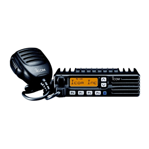
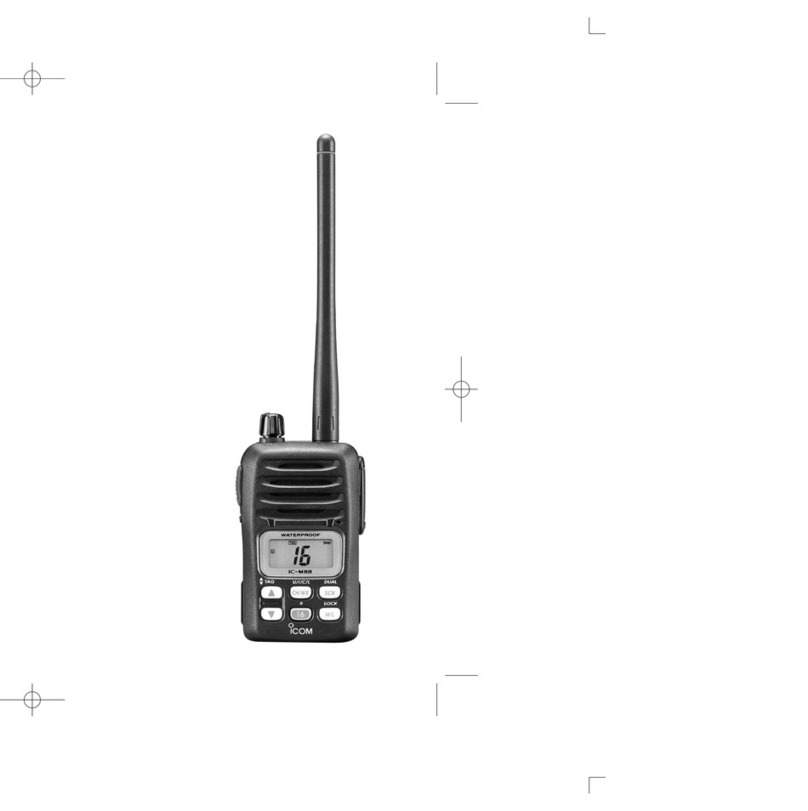
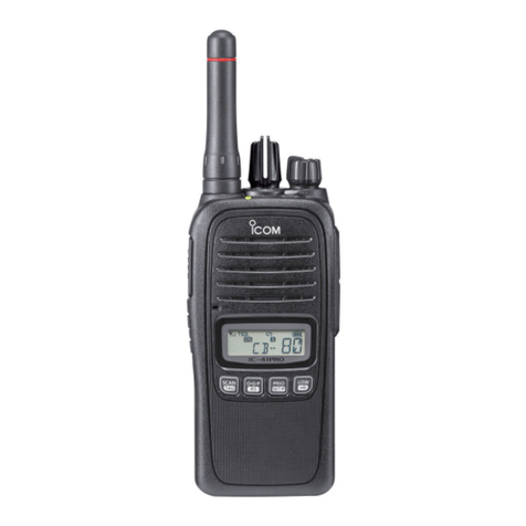
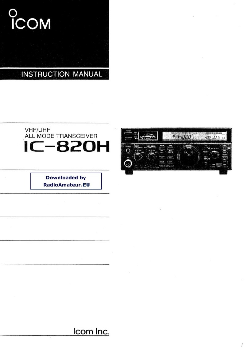
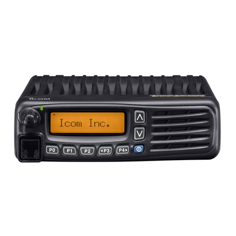
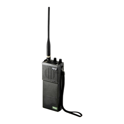
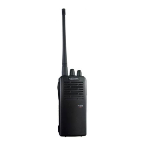
Icom IC-F33GT User manual

GUIDE FOR CD
1) COMPOSION
1
IC_F33_F43_series F33_F34.pdf
F43_F44.pdf
FYC F33_F34_A3format.pdf
F33_F34_A4format.pdf
F43_F44_A3format.pdf
F43_F44_A4format.pdf
F33_F43_MANUAL.pdf
F34_F44_MANUAL.pdf
Installer ar505eng.exe
W_README.txt
2) DESCRIPTION
F33_F34.pdf
The service manual for IC-F33/F34/GT/GS including all service information in this CD. This file is mainly used for viewing on the
computer display and checking page order to make printed service manual. Or when you want to find a component, you can
find very fast using “FIND” function (except Board Layout).
F43_F44.pdf
The service manual for IC-F43/F44/GT/GS including all service information in this CD. This file is mainly used for viewing on the
computer display and checking page order to make printed service manual. Or when you want to find a component, you can
find very fast using “FIND” function (except Board Layout).

2
F33_F34_A4format.pdf
F43_F44_A4format.pdf
Consists of A4 format pages (Circuit description, Adjustment procedures, Parts list, and etc.). This file is used for
printing out A4 format pages.
F33_F43_MANUAL.pdf
The instruction manual for IC-F33/F43/GT/GS. The contents of this file is exactly same as supplied instruction
manual with product and consists of all A4 format pages. If you have A4 format printer, you can print and make
brand new instruction manual any time you want. This file is also very helpful when you want to change or set
product setting condition for adjustment or else.
=========================================================================================
Icom, Icom Inc. and Icom logo are registered trademarks of Icom Incorporated (Japan) in the United states, the
United Kingdom, Germany, France, Spain, Russia and/or other countries.
Acrobat Reader Copyright © 1987-2002 Adobe Systems Incorporated. All rights reserved.
Adobe, the Adobe logo, Acrobat, and the Acrobat logo are trademarks of Adobe Systems Incorporated.
Microsoft and Windows are registered trademarks of Microsoft Corporation in the U.S.A. and other countries.
Copyright 2004 Icom Inc.
=========================================================================================
ar505eng.exe
ar505eng.exe is an installation program of Adobe Acrobat®Reader 5.0 (English version) for Microsoft®Windows®
95/98/Me/NT/2000/XP users.
W_README.txt
W_README.txt is a readme text about this service manual for Windows®user that not installed Acrobat®Reader
yet.
F34_F44_MANUAL.pdf
The instruction manual for IC-F34/F44/GT/GS. The contents of this file is exactly same as supplied instruction
manual with product and consists of all A4 format pages. If you have A4 format printer, you can print and make
brand new instruction manual any time you want. This file is also very helpful when you want to change or set
product setting condition for adjustment or else.
F33_F34_A3format.pdf
F43_F44_A3format.pdf
Consists of A3 format pages (Board layout, Mechanical parts and disassembly, and etc.). This file is used for
printing out A3 format pages.

VHF TRANSCEIVERS
SERVICE
MANUAL
COVER.indd1 10/27/200410:04:41AM

INTRODUCTION
DANGER
ORDERING PARTS
This service manual describes the latest service
information for the IC-F33GT/GS and IC-F34GT/GS VHF
TRANSCEIVERS at the time of publication.
NEVER connect the transceiver to an AC outlet or to a DC
power supply that uses more than 8 V. Such a connection
could cause a fire or electric hazard.
DO NOT expose the transceiver to rain, snow or any liquids.
DO NOT reverse the polarities of the power supply when
connecting the transceiver.
DO NOT apply an RF signal of more than 20 dBm (100 mW)
to the antenna connector. This could damage the trans-
ceiver's front end.
Be sure to include the following four points when ordering
replacement parts:
1. 10-digit order numbers
2. Component part number and name
3. Equipment model name and unit name
4. Quantity required
<SAMPLE ORDER>
5030002760 LCD FX-2721 LCD IC-F33GT Main unit 5 pieces
8810009220 Screw BO 2x8 ZK IC-F33GT/GS Chassis 10 pieces
Addresses are provided on the inside back cover for your
convenience.
1. Make sure a problem is internal before disassembling the transceiver.
2. DO NOT open the transceiver until the transceiver is disconnected from its power source.
3. DO NOT force any of the variable components. Turn them slowly and smoothly.
4. DO NOT short any circuits or electronic parts. An insulated turning tool MUST be used for all adjustments.
5. DO NOT keep power ON for a long time when the transceiver is defective.
6. DO NOT transmit power into a signal generator or a sweep generator.
7. ALWAYS connect a 30 dB to 40 dB attenuator between the transceiver and a deviation meter or spectrum analyzer when
using such test equipment.
8. READ the instructions of test equipment thoroughly before connecting equipment to the transceiver.
To upgrade quality, all electrical or mechanical parts and
internal circuits are subject to change without notice or
obligation.
Icom, Icom Inc. and are registered trademarks of Icom Incorporated (Japan) in the United States, the United Kingdom,
Germany, France, Spain, Russia and/or other countries.
MODEL CHANNEL SPACING SYMBOL FREQUENCY
IC–F33GT 15.0/30.0 kHz USA-01 136–174 MHz
12.5/25.0 kHz GEN-01 136–174 MHz
IC–F34GT 12.5/20.0/25.0 kHz EUR-01 136–174 MHz
IC–F33GS 15.0/30.0 kHz USA-01 136–174 MHz
12.5/25.0 kHz GEN-01 136–174 MHz
IC–F34GS 12.5/20.0/25.0 kHz EUR-01 136–174 MHz
REPAIR NOTES
COVER.indd2 10/26/20047:26:43PM

TABLE OF CONTENTS
SECTION 1 SPECIFICATIONS
SECTION 2 INSIDE VIEWS
SECTION 3 DISASSEMBLY INSTRUCTIONS
SECTION 4 CIRCUIT DESCRIPITON
4-1 RECEIVER CIRCUITS. . . . . . . . . . . . . . . . . . . . . . . . . . . . . . . . . . . . . . . . . . . . . . . . . . . . . . . . 4-1
4-2 TRANSMITTER CIRCUITS . . . . . . . . . . . . . . . . . . . . . . . . . . . . . . . . . . . . . . . . . . . . . . . . . . . . 4-3
4-3 PLL CIRCUITS . . . . . . . . . . . . . . . . . . . . . . . . . . . . . . . . . . . . . . . . . . . . . . . . . . . . . . . . . . . . . 4-4
4-4 POWER SUPPLY CIRCUITS. . . . . . . . . . . . . . . . . . . . . . . . . . . . . . . . . . . . . . . . . . . . . . . . . . . 4-4
4-5 OTHER CIRCUITS . . . . . . . . . . . . . . . . . . . . . . . . . . . . . . . . . . . . . . . . . . . . . . . . . . . . . . . . . . 4-5
4-6 PORT ALLOCATIONS . . . . . . . . . . . . . . . . . . . . . . . . . . . . . . . . . . . . . . . . . . . . . . . . . . . . . . . . 4-5
SECTION 5 ADJUSTMENT PROCEDURES
5-1 PREPARATION . . . . . . . . . . . . . . . . . . . . . . . . . . . . . . . . . . . . . . . . . . . . . . . . . . . . . . . . . . . . . 5-1
5-2 SOFTWARE ADJUSTMENTS . . . . . . . . . . . . . . . . . . . . . . . . . . . . . . . . . . . . . . . . . . . . . . . . . . 5-4
SECTION 6 PARTS LIST
SECTION 7 MECHANICAL PARTS AND DISASSEMBLY
SECTION 8 SEMICONDUCTOR INFORMATION
SECTION 9 BOARD LAYOUTS
9-1 MAIN UNIT . . . . . . . . . . . . . . . . . . . . . . . . . . . . . . . . . . . . . . . . . . . . . . . . . . . . . . . . . . . . . . . . 9-1
9-2 PA UNIT . . . . . . . . . . . . . . . . . . . . . . . . . . . . . . . . . . . . . . . . . . . . . . . . . . . . . . . . . . . . . . . . . . . 9-3
9-3 ANT UNIT . . . . . . . . . . . . . . . . . . . . . . . . . . . . . . . . . . . . . . . . . . . . . . . . . . . . . . . . . . . . . . . . . 9-3
9-4 FUSE UNIT . . . . . . . . . . . . . . . . . . . . . . . . . . . . . . . . . . . . . . . . . . . . . . . . . . . . . . . . . . . . . . . . 9-3
SECTION 10 BLOCK DIAGRAM
SECTION 11 VOLTAGE DIAGRAM
11-1 MAIN UNIT . . . . . . . . . . . . . . . . . . . . . . . . . . . . . . . . . . . . . . . . . . . . . . . . . . . . . . . . . . . . . . . . 11-1
11-2 PA/ANT/FUSE UNITS . . . . . . . . . . . . . . . . . . . . . . . . . . . . . . . . . . . . . . . . . . . . . . . . . . . . . . . . 11-3
CONTENTSSEC71.indd1 10/26/20047:31:57PM

■GENERAL
• Frequency coverage : 136.000–174.000 MHz
• Mode : FM
• Type of emission :
• Number of conventional channels : 256 ch, 16 banks
• Antenna impedance : 50 Ω(nominal)
• Operating temperature range : –30˚C to +60˚C (–22˚F to +140˚F) [USA], [GEN]
–25˚C to +55˚C [EUR]
• Power supply requirement : 7.2 V DC nominal (negative ground)
• Current drain (at 7.2 V DC) :
• Dimensions (projections not included) : 53.0(W) × 120.0(H) × 32.5(D) mm; 23⁄32(W) × 423⁄32(H) × 19⁄32(D) in
• Weight (with BP-231+FA-SC55V-1) : 285 g; 101⁄16 oz (Approx.)
■TRANSMITTER
• Output power (at 7.2 V DC) : High: 5 W, Low: 1 W
• Modulation : Variable reactance frequency modulation
• Maximum permissible deviation : ±5.0 kHz (Wide), ±4.0 kHz (Middle), ±2.5 kHz (Narrow)
• Frequency error : ±2.5 ppm
• Spurious emissions : 80 dB (typical) [USA], [GEN]
0.25 µW (≤1 GHz), 1.0 µW (≥1 GHz) [EUR]
• Adjacent channel power : 70 dB min (80 dB typical) for Wide and Middle
60 dB min (70 dB typical) for Narrow
• Audio harmonic distortion : 3% typical (Mod. 1 kHz, 40% deviation)
• Limiting charact of modulator : 60–100% of maximum deviation
• Microphone impedance : 2.2 kΩ
■RECEIVER
• Receive system : Double conversion superheterodyne system
• Intermediate frequencies : 1st IF: 46.35 MHz, 2nd IF: 450 kHz
• Sensitivity : 0.25 µV (–119 dBm) typical at 12 dB SINAD [USA], [GEN]
–4 dBµV (–111 dBm) emf typical at 20 dB SINAD [EUR]
• Adjacent channel selectivity : 70 dB min (75 dB typical) for Wide and Middle
60 dB min (65 dB typical) for Narrow
• Spurious response : 70 dB
• Intermodulation rejection ratio : 70 dB min (74 dB typical) [USA], [GEN]
65 dB min (67 dB typical) [EUR]
• Audio output power : 0.5 W typical at 5% distortion with an 8 Ωload
• Squelch sensitivity (at threshold) : 0.25 µV typical
• Output impedance (Audio) : 8 Ω
Specifications are measured in accordance with EIA-152-C/204D, TIA-603 or EN 300 086.
All stated specifications are subject to change without notice or obligation.
S SECTION 1 SPECIFICATIONS
1 - 1
VERSION WIDE MIDDLE NARROW
[USA], [GEN] 16K0F3E (25.0 kHz) N/A 11K0F3E (12.5 kHz)
[EUR] 14K0F3E (20.0 kHz) 8K50F3E (12.5 kHz)
RECEIVING TRANSMITTING
Stand-by Max. audio High (5 W) Low (1 W)
85 mA 300 mA 1.5 A 0.7 A

SECTION 2 INSIDE VIEWS
•MAIN UNIT
2 - 1
•PA UNIT
TX Mute switch
(Q501: UNR9213J)
PLL IC
(IC21: LMX2352TM)
Base band IC
(IC14: AK2346)
EEPROM
(IC10: 24LC64T-I/SN)
CPU
(IC22: HD64F2238BTF13)
R5 Regulator
(Q25: 2SA1577)
FM IF IC
(IC9: TA31136FN)
AF amplifier
(IC15: TA7368F)
APC amplifier
(IC2: TA75S01F) IF amplifier
(Q7: 2SC4215) TX/RX switch
(D16, D17: MA2S077)
+5 Regulator
(IC17: NJM2870)
T5 Regulator
(Q24: 2SA1577)
D/A converter
(IC12: M62364FP)
VCO circuits
TOP VIEW BOTTOM VIEW
S5 Regulator
Q26: 2SB1132
Q27: XP6501
Q28: UNR9113 J
Power amplifier
(Q701: RD07MVS1)
Drive amplifier
(Q702: RD01MUS1)
Antenna switch
(D701: 1SV307)
TOP VIEW BOTTOM VIEW
CONTENTSSEC71.indd4 10/26/20047:32:05PM

SECTION 3 DISASSEMBLY INSTRUCTIONS
3 - 1
Chassis unit E
A
B
C
D
F
Main shield
Main unit
K
K
J
J
L
J
I
GH
Chassis unit
M
N
N
•REMOVING THE CHASSIS UNIT
1 Unscrew 1 nut A, and remove 2 knobs B, C.
2 Unscrew 2 screws D.
3 Unscrew 2 screws E.
4 Take off the chassis unit in the direction of the arrow.
5 Unplug the connector Ffrom the chassis unit.
•REMOVING THE PA UNIT
1 Unscrew 3 screws M.
2 Unsolder 4 points N, and take off the PA unit in the
direction of the arrow.
•REMOVING THE MAIN UNIT
1 Unscrew 2 nuts G, and remove the top plate H.
2 Remove the side plate I.
3 Unscrew 6 screws J.
4 Unsolder 8 points K, and remove the main shield.
5 Unsolder 2 points L, and take off the main unit in the
direction of the arrow.
CONTENTSSEC71.indd5 10/26/20047:32:07PM

4 - 1
4-1 RECEIVER CIRCUITS
4-1-1 ANTENNA SWITCHING CIRCUIT (PA UNIT)
The antenna switching circuit functions as a low-pass filter
while receiving and a resonator circuit while transmitting.
This circuit does not allow transmit signals to enter the
receiver circuits.
Received signals enter the antenna connector (CHASSIS;
J1) and pass through the low-pass filter (ANT unit; L801,
L802, C803). The filtered signals are passed through the λ⁄4
type antenna switching circuit (D701, D704, D706) and then
applied to the RF circuit.
4-1-2 RF CIRCUIT (MAIN UNIT)
The RF circuit amplifies signals within the range of frequen-
cy coverage and filters out-of-band signals.
The signals from the antenna switching circuit pass through
the two-stage tunable bandpass filters (D19, D24, L7, L8,
C27, C369). The filtered signals are amplified at the RF
amplifier (Q5) and then passed through the another two-
stage tunable bandpass filters (D14, D15, L11, C39, C45)
to suppress unwanted signals. The filtered signals are
applied to the 1st mixer circuit.
D14, D15, D19 and D24 employ varactor diodes, that are
controlled by the CPU via the D/A converter (IC12), to track
the bandpass filter. These varactor diodes tune the center
frequency of an RF passband for wide bandwidth receiving
and good image response rejection.
SECTION 4 CIRCUIT DESCRIPTION
4-1-3 1ST MIXER AND 1ST IF CIRCUITS
(MAIN UNIT)
The 1st mixer circuit converts the received signal into fixed
frequency of the 1st IF signal with the PLL output frequency.
By changing the PLL frequency, only the desired frequency
passes through a monolithic filter at the next stage of the
1st mixer.
The RF signals from the bandpass filter are mixed with the
1st LO signals, where come from the RX VCO circuit, at the
1st mixer circuit (Q6) to produce a 46.35 MHz 1st IF sig-
nal. The 1st IF signal is passed through a monolithic filter
(FI1) to suppress out-of-band signals. The filtered signal is
applied to the 2nd IF circuit after being amplified at the 1st
IF amplifier (Q7).
4-1-4 2ND IF AND DEMODULATOR CIRCUITS
(MAIN UNIT)
The 2nd mixer circuit converts the 1st IF signal into a 2nd
IF signal. The double-conversion superheterodyne system
(which convert receive signals twice) improves the image
rejection ratio and obtains stable receiver gain.
The 1st IF signal from the IF amplifier (Q7) is applied to
the 2nd mixer section of the FM IF IC (IC9, pin 16), and is
mixed with the 2nd LO signal to be converted into a 450
kHz 2nd IF signal.
The FM IF IC (IC9) contains the 2nd mixer, limiter amplifier,
quadrature detector, active filter and noise amplifier circuits.
A 2nd LO signal (45.9 MHz) is produced at the PLL circuit
by tripling it’s reference frequency 15.3 MHz).
Mixer
16
Limiter
amp.
2nd IF filter
450 kHz X2
15.3 MHz
45.9 MHz
IC9 TA31136FN
12 1st IF from the IF amplifier (Q7)
"RSSI" signal to the CPU ( IC22, pin 50)
11109
87 5
AF signal "DET"
"SQLC" signal from the
D/A converter IC
(IC12, pin 2)
R5V
X1
2
Active
filter
Noise
detector
FM
detector
13
"NOIS" signal to the CPU (IC22, pin 75)
RSSI
Noise
amp.
Noise
comparator
×3
Q22
FI2
3
• 2ND IF DEMODULATOR CIRCUIT

4 - 2
The 2nd IF signal from the 2nd mixer (IC9, pin 3) passes
through the ceramic filter (FI2) to remove unwanted hetero-
dyned frequencies. It is then amplified at the limiter amplifier
section (IC9, pin 5) and applied to the quadrature detector
section (IC9, pins 10, 11) to demodulate the 2nd IF signal
into AF signals.
The demodulated AF signals are output from pin 9 (IC9) and
applied to the base band IC (IC14).
4-1-5 AF AMPLIFIER CIRCUIT (MAIN UNIT)
The AF amplifier circuit amplifies the demodulated AF sig-
nals to drive a speaker. This transceiver employs the base
band IC which is composed of pre-amplifier, expander,
scrambler, MSK de-modulator, etc. at the AF amplifier sec-
tion.
The AF signals from the FM IF IC (IC9, pin 9) are amplified
at the AF amplifier section in the base band IC (IC14, pin
23), and are then applied to the high-pass filter and low-
pass filter section of it.
The filtered signals pass through the high-pass filter to sup-
press unwanted harmonic components. The signals pass
through (or bypass) scrambler and expander sections. The
signals are amplified at the amplifier section in the base
band IC (IC14).
The output signals from IC14 (pin 20) pass through the low-
pass filter sector (IC23, pins 1, 2), and are then applied to
the AF amplifier (IC15, pin 8) via the AF volume (R315).
The power amplified AF signals are output from pin 10 and
applied to the internal speaker that is connected to J4 via [SP]
jack (J2).
4-1-6 SQUELCH CIRCUITS (MAIN UNIT)
• NOISE SQUELCH
A squelch circuit cuts out AF signals when no RF signals
are received. By detecting noise components in the AF sig-
nals, the squelch circuit switches the AF amplifier controller.
A portion of the AF signals from the FM IF IC (IC9, pin 9)
are passed through the D/A converter (IC12, pins 1, 2). The
signals are applied to the active filter section in the FM IF
IC (IC9, pin 8). The active filter section filters and amplifies
noise components. The amplified signals are converted into
the pulse-type signals at the noise detector section. The
detected signals output from pin 13 (NOIS) via the noise
comparator section.
The “NOIS” signal from the FM IF IC is applied to the CPU
(IC22, pin 75). Then the CPU analyzes the noise condition
and outputs AF mute control signal from pin 84 to control
the squelch switch (Q502) as the “MUTE” signal.
• CTCSS AND DTCS
The tone squelch circuit detects tone signals and opens the
squelch only when receiving a signal containing a matching
subaudible tone (CTCSS or DTCS). When tone squelch is in
use, and a signal with a mismatched or no subaudible tone
is received, the tone squelch circuit mutes the AF signals
even when noise squelch is open.
A portion of the “DET” AF signals from the FM IF IC (IC9,
pin 9) pass through the low-pass filter (IC19, pin 5) to
remove AF (voice) signals, and are then applied to the
amplifier (IC19, pin 3). The amplified signals are applied to
the CTCSS or DTCS decoder in the CPU (IC22, pin 46) via
the “CDEC” line. The CPU outputs AF mute control signal
from pin 84 to control the squelch switch (Q502) as the
“MUTE” signal.
Base band IC
(IC14)
"DET" AF signal
from FM IF IC (IC9, pin 9) 23 20 LPF
AF
volume
AF
AMP
IC15
Speaker
IC23
IC23
IC13
IC6 IC12 D12
Microphone
AMP
3
7
4
FM/PM switch
D/A converter FM mod.
LPF
"CTCSS/DTCS" signal from
D/A conveter IC (IC12, pin 11)
"TONE" signal from CPU via low-pass
filter (IC22, pin 43)
to TX VCO circuit
(Q16, D10, D13, D501)
3
• AF AND MIC AMPLIFIER CIRCUIT
4 - 3
4-2 TRANSMITTER CIRCUITS
4-2-1 MICROPHONE AMPLIFIER CIRCUIT
(MAIN UNIT)
The microphone amplifier circuit amplifies audio signals
within +6 dB/octave pre-emphasis characteristics from the
microphone to a level needed for the modulation circuit.
This transceiver employs the base band IC which is com-
posed of microphone amplifier, compressor, scrambler,
limiter, splatter filter, MSK modulator, etc. at the microphone
amplifier section.
The AF signals (MIC) from the microphone (MC1) are
applied to the amplifier (IC23, pins 6, 7). The amplified sig-
nals are amplified again at the microphone amplifier section
of the base band IC (IC14, pins 3). The amplified signals are
passed through or bypass the compressor, scrambler sec-
tions of IC14, and are then passed through the high-pass,
limiter amplifier, splatter filter sections of IC14.
The filtered AF signals from the base band IC (pin 6) are
applied to the FM/PM switch (IC13, pins 6, 7), and pass
through the low-pass filter (IC6, pins 1, 2). The filtered sig-
nals are applied to the D/A converter (IC12, pin 4). The out-
put signals from the D/A converter (IC12, pin 3) are applied
to the modulation circuit (D12).
4-2-2 MODULATION CIRCUIT (MAIN UNIT)
The modulation circuit modulates the VCO oscillating signal
(RF signal) using the microphone audio signals.
The AF signals from the D/A converter (IC12, pin 3) change
the reactance of varactor diode (D12) to modulate the oscil-
lated signal at the TX VCO circuit (Q16, D10, D13, D501).
The modulated VCO signal is amplified at the buffer ampli-
fiers (Q15, Q29) and is then applied to the drive amplifier
circuit via the T/R switch (D16).
The CTCSS/DTCS signals (“CENC0”, “CENC1”, ”CENC2")
from the CPU (IC22, pins 13, 15, 16) are combined at the
resistors (R222–R224) and are then pass through the low-
pass filter (IC6, pins 12, 14). The filtered signals are applied
to the D/A converter (IC12, pin 12) via the “TONC” line. The
output signals from the D/A converter (IC12, pin 11) are
mixed with the filtered Mic audio signals.
The mixed signals are passed through the D/A converter
(IC12, pin 3, 4), and are then applied to the D12 in the TX
VCO circuit.
4-2-3 DRIVE/POWER AMPLIFIER CIRCUITS
(PA UNIT)
The drive/power amplifier circuits amplify the TX VCO oscil-
lating signal to an output power level.
The signal from the TX VCO circuit passes through the T/R
switch (MAIN unit; D16), and is amplified at the YGR (Q704),
drive (Q702), power (Q701) amplifiers to obtain 5 W of RF
power (at 7.2 V DC).
The amplified signal is passed through the low-pass filter
(L703, L704, C708, C711, C768), power detector (D702,
D703), antenna switching circuit (D701) and another low-
pass filters (PA unit; L709, C744, C746, C769 / ANT unit;
L801, L802, C802, C803, C807), and is then applied to the
antenna connector (CHASSIS unit; J1).
The bias voltage of the drive (Q702) and power (Q701)
amplifiers are controlled by the APC circuit.
4-2-4 APC CIRCUIT (PA AND MAIN UNITS)
The APC circuit protects the drive and power amplifiers from
a mismatched output load and selects output power of HIGH
or LOW.
The power detector circuit (PA unit; D702, D703) detects the
transmit power output level and converts it into DC voltage.
The output voltage is at a minimum level when the antenna
impedance is matched with 50 Ωand is increased when it is
mismatched.
The detected voltage is applied to the differential amplifier
(MAIN unit; IC2; pin 3), and the “T2” signal from the D/A con-
verter (MAIN unit; IC12, pin 23), controlled by the CPU (MAIN
unit; IC22), is applied to the other input for reference. When
antenna impedance is mismatched, the detected voltage
exceeds the power setting voltage. Then the output voltage
of the differential amplifier (MAIN unit; IC2, pin 4) controls
the input bias voltage of the drive (PA unit; Q702) and power
(PA unit; Q701) amplifiers to reduce the output power.
• APC CIRCUIT
Power
amp.
APC
amp.
Driver
amp.
+
–
YGR
amp.
VCC
to ANT unit
PA unit
T2
TMUT
RF signal
from PLL circuit
T5V
APC control circuit
D703
D702
ANT
SW LPF
LPF
Q702
Q704
IC2
IC501
Q701
D701

4-3 PLL CIRCUITS
4-3-1 PLL CIRCUIT (MAIN UNIT)
A PLL circuit provides stable oscillation of the transmit fre-
quency and receive 1st LO frequency. The PLL output com-
pares the phase of the divided VCO frequency to the refer-
ence frequency. The PLL output frequency is controlled by
the divided ratio (N-data) of a programmable divider.
The PLL circuit contains the TX and RX VCO circuits (Q16,
Q17, D9–D11, D13, D500, D501). The oscillated signal is
amplified at the buffer amplifier (Q15). The output signal fre-
quency is doubled at Q14, and is then applied to the PLL IC
(IC21, pin 6) after being passed through the bandpass filter
(L32, C205, C507).
Q500, D502 and D503 switch the filtering frequencies
between TX and RX which is controlled by R5V.
The PLL IC contains a prescaler, programmable counter,
programmable divider and phase detector, etc. The applied
signal is divided at the prescaler and programmable counter
section by the N-data ratio from the CPU. The divided signal
is detected on phase at the phase detector using the refer-
ence frequency.
If the oscillated signal drifts, its phase changes from that of
the reference frequency, causing a lock voltage change to
compensate for the drift in the oscillated frequency.
4-3-2 VCO CIRCUITS (MAIN UNIT)
The VCO circuits contains a separate RX VCO (Q17, D9,
D11, D500) and TX VCO (Q16, D10, D13, D501). The oscil-
lated signal is amplified at the buffer amplifiers (Q15, Q29)
and is then applied to the T/R switch (D16, D17). Then the
receive 1st LO (Rx) signal is applied to the 1st mixer (Q6)
and the transmit (Tx) signal to the YGR amplifier circuit (PA
unit; Q704).
A portion of the signal from the buffer amplifier (Q15) is fed
back to the PLL IC (IC21, pin 6) via the doubler circuit (Q14)
as the comparison signal.
4-4 POWER SUPPLY CIRCUIT
4-1-1 MAIN UNIT VOLTAGE
LINE DESCRIPTION
VCC The voltage from the connected battery pack.
+5V
Common 5 V converted from the VCC line at the
+5 regulator circuit (IC17). The output voltage is
supplied to the buffer amplifiers (Q21), PLL IC
(IC21) etc.
S5V
Common 5 V converted from the VCC line at the
S5 regulator circuit (Q26–Q28). The output volt-
age is supplied to the ripple filter (Q20), etc.
R5V
Receive 5 V converted from the S5V line at the
R5 regulator circuit (Q25). The output voltage is
supplied to the tripler (Q22), FM IF IC (IC9), IF
amplifier (Q7), 1st mixer (Q6), RF amplifier (Q5),
etc.
T5V
Transmit 5 V converted from the S5V line at the
T5 regulator circuit (Q24). The output voltage is
supplied to the APC amplifier (IC2), PA unit, etc.
Shift register
Prescaler
Phase
detector
Loop
filter
Programmable
counter
Programmable
divider
X2
15.3 MHz
10
Buffer
Q15
Buffer
Q21
Buffer
Q29
×2
Q14
14
15
16
SCK
SO
PLST
to transmitter circuit
to 1st mixer circuit
D16
D17
46
Q16, D10, D13, D501
TX VCO
Q17, D9, D11, D500
RX VCO
IC21 LMX2352
3
45.9 MHz 2nd LO
signal to the FM IF IC
(IC9, pin 2) Tripler
Q22
"LVIN" signal
to the CPU
(IC22, pin 49)
BPF
• PLL CIRCUIT
4 - 4

4 - 5
4-5 OTHER CIRCUITS
4-5-1 COMPANDER CIRCUIT (MAIN UNIT)
IC-F33GT/GS/F34GT/GS have compander circuit which can
improve S/N ratio and become wide dynamic range. The cir-
cuit is composed in the base band IC (IC14).
(1) IN CASE OF TRANSMITTING
The audio signals from the microphone are applied to the
base band IC (IC14, pin 3) via microphone amplifier (IC23).
The signals are amplified at the amplifier section, and are
then applied to the compressor circuit to compress the audio
signals. The signals pass through (or bypass) scrambler sec-
tion, and are then applied to the limiter section after being
passed through the high-pass filter. The filtered signals pass
through the splatter filter section, and are then applied to the
modulation circuit (D12) via the FM/PM switch (IC13), low-
pass filter (IC6) and D/A converter (IC12).
(2) IN CASE OF RECEIVING
The demodulated AF signals from the IF IC are applied to
the amplifier section in base band IC (IC14, pin 23), and
then pass through the low-pass and high-pass filter sec-
tion to suppress unwanted signals. The filtered signals pass
through (or bypass) scrambler section, and are then applied
to the expander circuit to expand AF signals. The signals are
applied to the base band IC’s amplifier section (IC14, pins
19, 20), and are then applied to the AF amplifier circuit.
Pin
Number
Port
name Description
10 BAL
Outputs the modulation balance level
control signal. The signal is applied to
the buffer amplifier (IC24, pin 1).
14 TLVA Outputs the TX VCO lock voltage
control signal.
15 RLVA Outputs the RX VCO lock voltage
control signal.
22 T1
Outputs the bandpass filter tuning
control signal . The output signal is
applied to the bandpass filters (D19,
D240).
23 T2
• Outputs the bandpass filter tuning
control signal . The output signal is
applied to the bandpass filters (D14,
D15).
• Outputs the TX control signal . The
output signal is applied to the APC
amplifier (IC2, pin 1).
Scrambler/
De-scrambler
TX/RX
HPF
Pre-
emphasis Limiter Splatter VR2
Expander VR4
RXA2
SMF
De-
emphasis
Com-
pressor
VR1
(HPF)
RX
LPF
VR3
(HPF)
7 MOD
18
19
20 SIGNAL
3TXIN
23RXIN
21SDEC
10
14MDIR
9
MTDT
MTCK
13MSCK
11MDIO
12MRDF
MSK
Modulator
MSK
Demodulator
MSK
BPF
Control
Register
TXA1
RXA1
4-6 PORT ALLOCATIONS
4-6-1 D/A CONVERTOR IC (IC12)
• BASE BAND IC BLOCK DIAGRAM

4 - 6
Pin
number
Port
name Description
13, 15,
16
CENC0–
CENC2
Output the CTCSS/DTCS signals.
29 REF
Outputs the reference oscillator cor-
recting voltage. The voltage is applied
to the buffer amplifier (IC24, pin 3)
30 PLST Outputs strobe signals to the PLL IC
(IC21, pin 16).
34 PMFM
Outputs the FM/PM modulation
switching signal to the FM/PM switch
(IC13, pin 5).
35 MDIO
I/O port for the serial data signals
from/to the base band IC (IC14,
pin 11).
36 MSCK Outputs clock signal for the base
band IC (IC14, pin 13).
37 MDIR Outputs serial data control signal to
the base band IC (IC14, pin 14).
38 MTCK
Input port for transmitting MSK clock
signal from the base band IC (IC14,
pin 9).
39 MTDT Outputs MSK data for transmitting to
the base band IC (IC14, pin 10).
40 MRDF
Input port for the receiving MSK de-
tection signal from the base band IC
(IC14, pin 12).
41 DAST Outputs strobe signals to the D/A
convertor (IC12, pin 6).
43 SENC Output single tone encoder signal.
44 BEEP Outputs beep audio signals.
45 SDEC
Input port for single tone decode
signal from the base band IC (IC14,
pin 21).
46 CDEC Input port for CTCSS/DTCS signal
from the amplifier (IC19, pin 1).
48 BATV Input port for the detect signal for
connecting battery pack’s voltage.
49 LVIN Input port for the PLL lock voltage.
50 RSSI Input port for the S-meter signal from
the FM IF IC (IC9, pin 12).
51 TEMP Input port for the transceiver’s internal
temperature detecting signal.
69 CSFT Outputs shift signal for reference os-
cillator’s frequency.
70 AFON
Outputs audio control signal.
Low: While outputs audio signals
from the speaker.
Pin
Number
Port
name Description
74 PTT
Input port for the PTT switch detec-
tion signal.
Low: While the PTT switch is
pushed.
75 NOIS Input port for the noise signal from
the FM IF IC (IC9, pin 13).
76 SO
Outputs serial data to the PLL IC
(IC21, pin 15) and D/A convertor
(IC12, pin 8).
78 SCK
Outputs serial clock signal to the PLL
IC (IC21 pin 14), D/A convertor (IC12,
pin 7), etc.
79 CLI Input port for the cloning data signal.
80 CLO Outputs the cloning data signal.
82 ESDA I/O port for data signals from/to the
EEPROM (IC10, pin 5).
84 MUTE Outputs AF control signal .
Low: While Squelch ON.
85 ESCL Outputs clock signal to the EEPROM
(IC10, pin 6).
86 S5C
Outputs the S5 regulator (Q26–Q28)
control signal.
Low: While the S5 regulator out-
puts 5 V voltage.
87 T5C
Outputs the T5 regulator (Q24) con-
trol signal.
Low: While transmitting.
88 R5C
Outputs the R5 regulator (Q25) con-
trol signal.
Low: While receiving.
89 TMUT
Outputs the transmitting mute switch
control signal to the mute switch
(Q 501).
High: While muting.
4-6-2 CPU (MAIN unit; IC22)

EQUIPMENT GRADE AND RANGE EQUIPMENT GRADE AND RANGE
DC power supply Output voltage
Current capacity
: 7.2 V DC
: 5 A or more Audio generator Frequency range
Measuring range
: 300–3000 Hz
: 1–500 mV
FM deviation meter Frequency range
Measuring range
: DC–800 MHz
: 0 to ±10 kHz Attenuator Power attenuation
Capacity
: 20 or 30 dB
: 10 W
Frequency counter
Frequency range
Frequency accuracy
Sensitivity
: 0.1–300 MHz
: ±1 ppm or better
: 100 mV or better
Standard signal
generator (SSG)
Frequency range
Output level
: 100–800 MHz
: 0.1 µV to 32 mV
(–127 to –17 dBm)
Digital multimeter Input impedance : 10 MΩ/V DC or better AC millivoltmeter Measuring range : 10 mV–10 V
RF power meter
Measuring rang
Frequency range
Impedance
SWR
: 1–10 W
: 100–800 MHz
: 50 Ω
: Better than 1.2 : 1
Oscilloscope Frequency rang
Measuring range
: DC–20 MHz
: 0.01–20 V
SECTION 5 ADJUSTMENT PROCEDURES
5 - 1
5-1 PREPARATION
When adjusting IC-F33GT/F33GS/F34GT/F34GS, the optional CS-F33G ADJ ADJUSTMENT SOFTWARE (Rev. 1.0 or later),
OPC-478 CLONING CABLE (RS-232C type), OPC-478U CLONING CABLE (USB type) and a JIG CABLE (see illustration at page 5-3)
are required.
▄SYSTEM REQUIREMENTS
• Microsoft®Windows®98/98SE/Me/2000
• RS-232C serial port (D-sub 9 pin)
• USB port
▄ ADJUSTMENT SOFTWARE INSTALLATION
qBoot up Windows.
- Quit all applications when Windows is running.
wInsert the cloning software CD into the appropriate CD
drive.
eSelect ‘Run’ from the [Start] menu.
rType the setup program name using the full path name,
then push [Enter] key.
(For example; D:\Setup.exe)
tFollow the prompts.
yProgram group ‘CS-F33G ADJ’ appears in the ‘Programs’
folder of the [Start] menu.
▄ BEFORE STARTING SOFTWARE ADJUSTMENT
Program the adjustment frequencies into the transceiver
using with the CS-F33G before starting the software adjust-
ment. Otherwise, the transceiver can not start software ad-
justment.
CAUTION!: BACK UP the originally programmed mem-
ory data in the transceiver before program-
ming the adjustment frequencies.
When program the adjustment frequencies into
the transceiver, the transceiver’s memory data
will be overwritten and lose original memory
data at the same time.
Microsoft and Windows are registered trademarks of
Microsoft Corporation in the U.S.A. and other countries.
▄
STARTING SOFTWARE ADJUSTMENT
qConnect the transceiver and PC with the OPC-478/U and
JIG CABLE.
wTurn the transceiver power ON.
eBoot up Windows, and click the program group ‘CS-F33G
ADJ’ in the ‘Programs’ folder of the [Start] menu, then
CS-F33G ADJ’s window appears.
rClick ‘Connect’ on the CS-F33G’s window, then appears
the transceiver’s adjustment screen.
tSet or modify adjustment data as desired.
▄ REQUIRED TEST EQUIPMENT
CH FREQUENCY ADJUSTMENT ITEM
1 155.000 MHz TX power
Bandwidth
: High
: Wide
2 155.000 MHz TX power
Bandwidth
: Low 2
: Wide
3 155.000 MHz TX power
Bandwidth
: Low
: Wide
4 155.000 MHz TX power
Bandwidth
: High
: Narrow
5 136.000 MHZ TX power
Bandwidth
: High
: Wide
6 155.000 MHz
TX power
CTCSS
DTCS
Bandwidth
: High
: 151.4 Hz
: 007
: Wide
7 174.000 MHz TX power
Bandwidth
: High
: Wide
8 155.000 MHz TX power
Bandwidth
: High
: Middle
• ADJUSTMENT FREQENCY LIST

5 - 2
q: Transceiver's connection state
w: Reload adjustment data
e: Receive sensitivity measurement
r: Connected DC voltage measurement
t: PLL lock voltage measurement
y: Operating channel select
u: RF output power
i: FM modulation balance (Narrow)
o: FM deviation (Narrow)
!0: FM deviation (Wide/Middle)
NOTE:
!1: CTCSS/DTCS deviation
!2: Squelch level
!3: Reference frequency
!4: Receive sensitivity (automatic)
!5: PLL lock voltage for RX (automatic)
!6: PLL lock voltage for TX (automatic)
!7: PLL lock voltage for RX (manual)
!8: PLL lock voltage for TX (manual)
!9: S-meter adjustment
The above values for settings are example only.
Each transceiver has its own specific values for each setting.
r
t
y
u
q
i
o
!0
!1
!4
!3
!2
!5
!6 !7
!8
!9
w
e
• CS-F33G ADJ'S SCREEN EXAMPLE

FM
deviation meter
SINAD meter
Speaker (8 Ω)
Audio generator
AC millivoltmeter
to the antenna connector
Attenuator
20 dB or 30 dB
RF power meter
0.1−10 W/50 Ω
Frequency
counter
Standard signal generator
0.1 µV to 32 mV
(−127 dBm to −17 dBm)
CAUTION!
DO NOT transmit while
an SSG is connected to
the antenna connector.
To [SP]
IC-F33G/F34G
To [MIC]
JIG cable
PC
to USB port
to RS-232C port
OPC-478 (RS-232C type)
OPC-478U (USB type)
OPC-478/OPC478U
JIG cable
To IC-F33G/F34G
[SP] jack
3-conductor 3.5(d) mm (1⁄8") plug
(SP + )
(CLONE)
(GND)
(SPE − )
5 - 3
• CONNECTION
• JIG CABLE

5 - 4
ADJUSTMENT ADJUSTMENT CONDITION MEASUREMENT VALUE
UNIT LOCATION
PLL LOCK
VOLTAGE
[LV (RX LVA)]
[LV (TX LVA)]
1 • Operating Channel : CH7
• Receiving
PC
screen
Check the "LVIN" item on the
CS-F33G ADJ's screen.
3.5 V
3.5 V
2 • Operating Channel : CH7
• Transmitting
CONVENIENT:
The PLL lock voltage can be adjustment automatically.
Set the cursor to "RX LVA"/"TX LVA" and then push [ENTER] key.
3 • Operating Channel : CH5
• Receiving
PC
screen
Check the "LVIN" item on the
CS-F33G ADJ's screen.
1.0–1.6 V
(Verify)
4 • Operating Channel : CH5
• Transmitting
1.0–1.6 V
(Verify)
REFERENCE
FREQUENCY
[REF]
1 • Operating Channel : CH7
• Connect the RF power meter or 50 Ω dummy
load to the antenna connector.
• Transmitting
Top
panel
Loosely couple the frequency
counter to the antenna con-
nector.
174.0000 MHz
OUTPUT
POWER
[Power (Hi)]
1 • Operating Channel : CH1
• Transmitting
Top
panel
Connect the RF power meter
to the antenna connector.
5.0 W
[Power (L2)] 2 • Operating Channel : CH2
• Transmitting
2.0 W
[Power (L1)] 3 • Operating Channel : CH3
• Transmitting
1.0 W
MODULATION
BALANCE
[BAL]
1 • Operating Channel : CH4
• No audio applied to the [MIC] connector.
• Set the FM deviation meter as:
HPF : OFF
LPF : 20 kHz
De- emphasis : OFF
Detector : (P–P)/2
• Push [P0] while transmitting
Top
panel
Connect the FM deviation
meter with the oscilloscope
to the antenna connector
through the attenuator.
Set to square wave
form
FM
DEVIATION
[MOD N]
(Narrow)
1• Operating Channel : CH4
• Set the FM deviation meter as:
HPF : OFF
LPF : 20 kHz
De- emphasis : OFF
Detector : (P–P)/2
• Connect the audio generator to the [MIC]
connector and set as
: 1.0 kHz/150 mVrms
• Transmitting
Top
panel
Connect the FM deviation
meter to the antenna connec-
tor through the attenuator.
±2.10 kHz
[MOD Ratio]
(Wide)
2• Operating Channel : CH1
• Transmitting
±4.10 kHz
[MOD Ratio]
(Middle)
(F34G only)
3• Operating Channel : CH8
• Transmitting
±3.20 kHz
CTCSS/DTCS
DEVIATION
[CTCSS/DTCS]
1• Operating Channel : CH6
• No audio applied to the [MIC] connector.
• Transmitting
Top
panel
Connect the FM deviation
meter to the antenna connec-
tor through the attenuator.
±0.70 kHz
5-2 SOFTWARE ADJUSTMENT (TRANSMITTING)
Select an operation using [↑] / [↓]keys, then set specified value using [←] / [→] keys on the connected computer keyboard

5 - 5
ADJUSTMENT ADJUSTMENT CONDITION MEASUREMENT VALUE
UNIT LOCATION
RX
SENSITIVITY
[BPF T1]
[BPF T2]
1• Operating Channel : CH5
• Connect the SSG to the antenna connector
and set as:
Frequency : 136.000 MHz
Level : 10 µV* (–87 dBm)
Modulation : 1 kHz
Deviation : ±3.5 kHz
• Receiving
PC
screen
Connect the SINAD meter
with an 8 Ωload to the [SP]
jack through the JIG cable.
Minimum distortion
level
CONVENIENT:
The BPF T1, BPF T2 can be adjustment automatically.
q-1: Set the cursor to "BPF ALL" and then push [ENTER] key.
q-2: The connected PC tunes BPF T1, T2 to peak levels.
or
w-1: Set the cursor to one of BPF T1, T2 as desired.
w-2: Push [ENTER] key to start tuning.
w-3: Repeat w-1 and w-2 to perform additional BPF tuning.
S-METER
[S-METER] 1• Operating Channel : CH5
• Connect the SSG to the antenna connector
and set as:
Frequency : 136.000 MHz
Level : 14 µV* (–84 dBm)
Modulation : 1 kHz
Deviation : ±3.5 kHz
• Receiving
Push the [ENTER] key on the connected computer's key-
board to set "L2" level.
2• Set the SSG as:
Level : 0.45 µV* (–114 dBm)
• Receiving
Push the [ENTER] key on the connected computer's key-
board to set "L0" level.
SQUELCH
LEVEL
[SQL]
1 • Operating Channel : CH1
• Connect the SSG to the antenna connector
and set as:
Frequency : 155.000 MHz
Level : 0.2 µV* (–121 dBm)
Modulation : 1 kHz
Deviation : ±3.5 kHz
• Receiving
Side
panel
Connect speaker to the [SP]
jack through the JIG cable.
Set SQL level to
close squelch.
Then set SQL level
at the point where
the audio signals
just appears.
*The output level of the standard signal generator (SSG) is indicated as the SSG's open circuit.
SOFTWARE ADJUSTMENT (RECEIVING)
• Select an operation using [↑] / [↓]keys, then set specified value using [←] / [→] keys on the connected computer keyboard
• Need to adjust "S-METER ADJUSTMENT" after "RX SENSITIVITY ADJUSTMENT" is adjusted.
Otherwise , "S-METER ADJUSTMENT" will not be adjusted properly.

6 - 1
SECTION 6 PARTS LIST
M.=Mounted side (T: Mounted on the Top side, B: Mounted on the Bottom side)
[MAIN UNIT]
REF ORDER DESCRIPTION M. H/V
NO. NO.
LOCATION
[MAIN UNIT]
REF ORDER DESCRIPTION M. H/V
NO. NO.
LOCATION
IC2 1110002750 S.IC TA75S01F (TE85R) T 88.1/12.4
IC6 1110005340 S.IC NJM12902V-TE1 B 55.4/23.8
IC8 1110005770 S.IC S-80942CNMC-G9C-T2 B 20.8/41.5
IC9 1110003200 S.IC TA31136FN (EL) T 81.5/17
IC10 1130011580 S.IC 24LC64T-I/SN B 29.7/13.2
IC12 1190001350 S.IC M62364FP 600D B 38.9/26.2
IC13 1130006220 S.IC TC4W53FU (TE12L) B 47.1/24
IC14 1110006220 S.IC AK2346-E2 B 41.5/13.2
IC15 1110001810 S.IC TA7368F (ER) T 97.3/15.4
IC17 1110005350 S.IC NJM2870F05-TE1 B 93.2/20.2
IC19 1110005330 S.IC NJM12904V-TE1 B 42.9/39.6
IC20 1130009090 S.IC LC75834W-TLM T 57.3/20.3
IC21 1130010100 S.IC LMX2352 T 79.5/34.1
IC22 1140011510 S.IC HD64F2238BTF13 B 17.4/22.4
IC23 1110005330 S.IC NJM12904V-TE1 B 36.9/39.3
IC24 1110002750 S.IC TA75S01F (TE85R) B 56.2/36.9
IC25 1130007020 S.IC TC7S66FU (TE85R) B 58.2/33
Q2 1590003320 S.FET TPC6103 (TE85L) T 98.4/4.8
Q3 1590003290 S.TR UNR9213J-(TX) T 93.4/5
Q4 1560000840 S.FET 2SK1829 (TE85R) T 90.9/34.7
Q5 1580000730 S.FET 3SK293 (TE85L) B 90.9/39
Q6 1580000760 S.FET 3SK299-T1 U73 B 86.8/29.5
Q7 1530002600 S.TR 2SC4215-O (TE85R) B 89.2/19.7
Q14 1530003260 S.TR 2SC5006-T1 B 78.7/34.3
Q15 1530003260 S.TR 2SC5006-T1 B 74.9/28.1
Q16 1530003260 S.TR 2SC5006-T1 B 76.6/25.1
Q17 1530003260 S.TR 2SC5006-T1 B 76.1/33.9
Q18 1590001400 S.TR XP1214 (TX) T 73.7/27.9
Q19 1590003290 S.TR UNR9213J-(TX) T 73.9/25.6
Q20 1530002850 S.TR 2SC4116-BL (TE85R) T 86.5/25.6
Q21 1560000540 S.FET 2SK880-Y (TE85R) T 70.8/23.8
Q22 1530002850 S.TR 2SC4116-BL (TE85R) T 81.3/24.3
Q24 1510000920 S.TR 2SA1577 T106 Q B 63.3/14.3
Q25 1510000920 S.TR 2SA1577 T106 Q B 64.4/10.4
Q26 1520000450 S.TR 2SB1132 T100 Q B 56.6/11.3
Q27 1590001190 S.TR XP6501-(TX) .AB B 57.5/7.3
Q28 1590003230 S.TR UNR9113J-(TX) B 54.1/7.1
Q29 1530003260 S.TR 2SC5006-T1 B 78.8/23.1
Q38 1590003290 S.TR UNR9213J-(TX) B 81.8/39.2
Q40 1590003290 S.TR UNR9213J-(TX) B 49.5/18.4
Q41 1590001190 S.TR XP6501-(TX) .AB T 90.8/21.3
Q42 1520000450 S.TR 2SB1132 T100 Q T 89.3/17.2
Q43 1590003400 S.TR UNR9112J T 77.7/4.9
Q44 1590003270 S.TR UNR9210J-(TX) B 29.8/5.8
Q45 1590003230 S.TR UNR9113J-(TX) T 54.6/4.5
Q500 1590003290 S.TR UNR9213J-(TX) T 78.6/23.7
Q501 1590003290 S.TR UNR9213J-(TX) T 84.7/11.9
Q502 1560001360 S.FET 2SK3019 TL B 36/11.7
D5 1160000060 S.DIO DAN202U T106 T 93.6/7.3
D6 1790001260 S.DIO MA2S077-(TX) B 27.6/31
D8 1790001250 S.DIO MA2S111-(TX) T 86.7/28.6
D9 1750000770 S.VCP HVC376BTRF B 69.4/30.5
D10 1750000770 S.VCP HVC376BTRF B 69.1/26.5
D11 1750000720 S.VCP HVC375BTRF B 73.3/33.7
D12 1720000470 S.VCP 1SV239 (TPH3) B 72/28.4
D13 1750000720 S.VCP HVC375BTRF B 73.5/23.1
D14 1750000710 S.VCP HVC350BTRF B 86.1/35.4
D15 1750000710 S.VCP HVC350BTRF B 87.4/39.5
D16 1790001260 S.DIO MA2S077-(TX) B 84.3/18
D17 1790001260 S.DIO MA2S077-(TX) B 83.4/22.2
D18 1790001250 S.DIO MA2S111-(TX) T 92.9/36.6
D19 1750000720 S.VCP HVC375BTRF B 94.8/39.1
D20 1790001240 S.DIO MA2S728-(TX) B 94.9/33.4
D21 1160000060 S.DIO DAN202U T106 B 28.4/22.6
D24 1750000720 S.VCP HVC375BTRF B 96.6/37.7
D25 1790001240 S.DIO MA2S728-(TX) B 94.9/34.7
D28 1790001670 S.DIO RB706F-40T106 B 29.8/2.9
D500 1750000770 S.VCP HVC376BTRF B 68.2/32.2
D501 1750000770 S.VCP HVC376BTRF B 68.1/24.9
D502 1790001260 S.DIO MA2S077-(TX) B 79.9/28.1
D503 1790001260 S.DIO MA2S077-(TX) T 80.2/26.7
D504 1750000940 S.DIO ISS400 TE61 B 28.2/24.5
FI1 2030000150 S.MLH FL-335 (46.350 MHz) T 91.3/27.1
FI2 2020001530 CER CFWLB450KFFA-B0 (GFWM450F)
X1 6070000190 S.DCR CDBCB450KCAY24-R0 B 80/16.9
X2 6050011930 S.XTL CR-781 (15.3 MHz) B 63.3/38.3
X5 6050011730 S.XTL CR-765 (3.6864 MHz) B 38.3/4
X6 6050011830 S.XTL CR-774 (12.288 MHz) B 30.9/31.5
L7 6200008090 S.COL LQW2BHN68NJ01L B 99.2/38.1
L8 6200008090 S.COL LQW2BHN68NJ01L B 93.1/40.3
L9 6200007750 S.COL LQW2BHN56NJ01L B 88.7/36.5
L11 6200007750 S.COL LQW2BHN56NJ01L B 85.9/33.8
L12 6200009350 S.COL ELJRE R22G-F3 B 84.3/26.5
L13 6200007850 S.COL ELJNC R82K-F B 89.4/32
L21 6200011030 S.COL ELJRF R10JF2 (0.1) B 80.5/22.8
L22 6200011030 S.COL ELJRF R10JF2 (0.1) B 77.2/28.5
L24 6200003640 S.COL MLF1608E 100K-T B 70.3/26.6
L25 6200007760 S.COL LQW2BHN82NJ01L B 71.9/23.5
L27 6200003550 S.COL MLF1608A 4R7K-T T 68.7/26.7
L28 6200003550 S.COL MLF1608A 4R7K-T T 68.8/30.4
L31 6200007000 S.COL ELJRE 82NG-F B 95.3/31.3
L32 6200007910 S.COL ELJRF 18NJF2 (18) T 77.8/27.4
L33 6200004480 S.COL MLF1608D R82K-T T 81.4/22.4
L35 6200003540 S.COL MLF1608D R22K-T T 84.6/25.5
L37 6200008090 S.COL LQW2BHN68NJ01L B 71.6/33.4
L41 6200007910 S.COL ELJRF 18NJF2 (18) B 80.2/33.5
L42 6200003550 S.COL MLF1608A 4R7K-T T 71.2/34.2
L43 6200003550 S.COL MLF1608A 4R7K-T T 69.4/21.9
L47 6200007720 S.COL LQW2BHN33NJ01L B 69.1/34.3
L48 6200008090 S.COL LQW2BHN68NJ01L B 69.3/22.7
L500 6200003640 S.COL MLF1608E 100K-T B 70.6/30.4
L501 6200003960 S.COL MLF1608A 1R0K-T T 74.7/31.9
L502 6200011000 S.COL ELJRF 56NJF2 (56) B 86.3/25.4
R1 7030005530 S.RES ERJ2GEJ 100 X (10 Ω) T 87.4/14.6
R4 7030007570 S.RES ERJ2GEJ 122 X (1.2 kΩ) T 86.3/9.7
R5 7030007340 S.RES ERJ2GEJ 153 X (15 kΩ) T 86.6/8.1
R6 7030005070 S.RES ERJ2GEJ 683 X (68 kΩ) T 86/15.7
R7 7030005310 S.RES ERJ2GEJ 124 X (120 kΩ) T 85.5/13.4
R8 7030005110 S.RES ERJ2GEJ 224 X (220 kΩ) T 88/10.2
R9 7030004990 S.RES ERJ2GEJ 221 X (220 Ω) T 90.5/12.3
R12 7030005530 S.RES ERJ2GEJ 100 X (10 Ω) B 90.2/36.8
R13 7030005090 S.RES ERJ2GEJ 104 X (100 kΩ) T 95.2/40.2
R15 7030005310 S.RES ERJ2GEJ 124 X (120 kΩ) T 92.2/39.3
R16 7030008280 S.RES ERJ2GEJ 271 X (270 Ω) B 89.8/41.2
R17 7030004970 S.RES ERJ2GEJ 470 X (47 Ω) T 88.7/36.8
R18 7030005040 S.RES ERJ2GEJ 472 X (4.7 kΩ) T 70.8/30.1
R19 7030005090 S.RES ERJ2GEJ 104 X (100 kΩ) T 91.1/37.6
R21 7030005090 S.RES ERJ2GEJ 104 X (100 kΩ) T 87.3/41.4
R22 7030005050 S.RES ERJ2GEJ 103 X (10 kΩ) T 88.5/38.9
R23 7030005090 S.RES ERJ2GEJ 104 X (100 kΩ) T 86.5/35.6
R24 7030005120 S.RES ERJ2GEJ 102 X (1 kΩ) B 86.2/22.8
R25 7030005120 S.RES ERJ2GEJ 102 X (1 kΩ) B 85.7/31.2
R29 7030007270 S.RES ERJ2GEJ 151 X (150 Ω) B 89.2/27.5
R31 7030004980 S.RES ERJ2GEJ 101 X (100 Ω) T 89.2/33.7
R32 7030010040 S.RES ERJ2GE-JPW T 92.2/31.9
R33 7030007280 S.RES ERJ2GEJ 331 X (330 Ω) B 90.2/22.9
R34 7030005090 S.RES ERJ2GEJ 104 X (100 kΩ) B 88.6/21.6
R35 7030004980 S.RES ERJ2GEJ 101 X (100 Ω) B 87.2/21.2
R36 7030005030 S.RES ERJ2GEJ 152 X (1.5 kΩ) B 81.9/12.6
R38 7030005090 S.RES ERJ2GEJ 104 X (100 kΩ) T 81.8/12.2
R39 7030004970 S.RES ERJ2GEJ 470 X (47 Ω) B 81.4/11.6
R40 7030007270 S.RES ERJ2GEJ 151 X (150 Ω) T 81.8/21.3
R43 7030004970 S.RES ERJ2GEJ 470 X (47 Ω) T 77.8/14.1
R44 7030005240 S.RES ERJ2GEJ 473 X (47 kΩ) T 77.9/21.3
R45 7030008290 S.RES ERJ2GEJ 183 X (18 kΩ) T 77.2/17.9
R46 7030005000 S.RES ERJ2GEJ 471 X (470 Ω) T 76.6/20.7
R48 7030005010 S.RES ERJ2GEJ 681 X (680 Ω) B 87.2/19.9
R50 7030005120 S.RES ERJ2GEJ 102 X (1 kΩ) B 84.9/22.8
R68 7030005120 S.RES ERJ2GEJ 102 X (1 kΩ) B 85.6/15.9
R69 7030005050 S.RES ERJ2GEJ 103 X (10 kΩ) B 85.6/18.2
R70 7030004980 S.RES ERJ2GEJ 101 X (100 Ω) B 80.1/26.4
R71 7030005070 S.RES ERJ2GEJ 683 X (68 kΩ) B 80.1/25.5
R72 7030005090 S.RES ERJ2GEJ 104 X (100 kΩ) B 35.5/34.2
R73 7030008010 S.RES ERJ2GEJ 123 X (12 kΩ) B 39.1/19.5
R74 7030006610 S.RES ERJ2GEJ 394 X (390 kΩ) B 40.1/19.5
R75 7030005240 S.RES ERJ2GEJ 473 X (47 kΩ) B 78.5/31
R76 7030004980 S.RES ERJ2GEJ 101 X (100 Ω) B 78.7/32
R77 7030004980 S.RES ERJ2GEJ 101 X (100 Ω) B 77.2/30.9
R78 7030005090 S.RES ERJ2GEJ 104 X (100 kΩ) B 75.9/29.7
R79 7030008340 S.RES RR0510P-182-D (1.8 kΩ) B 76.1/32.4
R80 7030005050 S.RES ERJ2GEJ 103 X (10 kΩ) T 75.1/23.9
R81 7030005090 S.RES ERJ2GEJ 104 X (100 kΩ) B 47.9/20.8
S.=Surface mount
Other manuals for IC-F33GT
3
This manual suits for next models
4
Table of contents
Other Icom Transceiver manuals