4 - 3
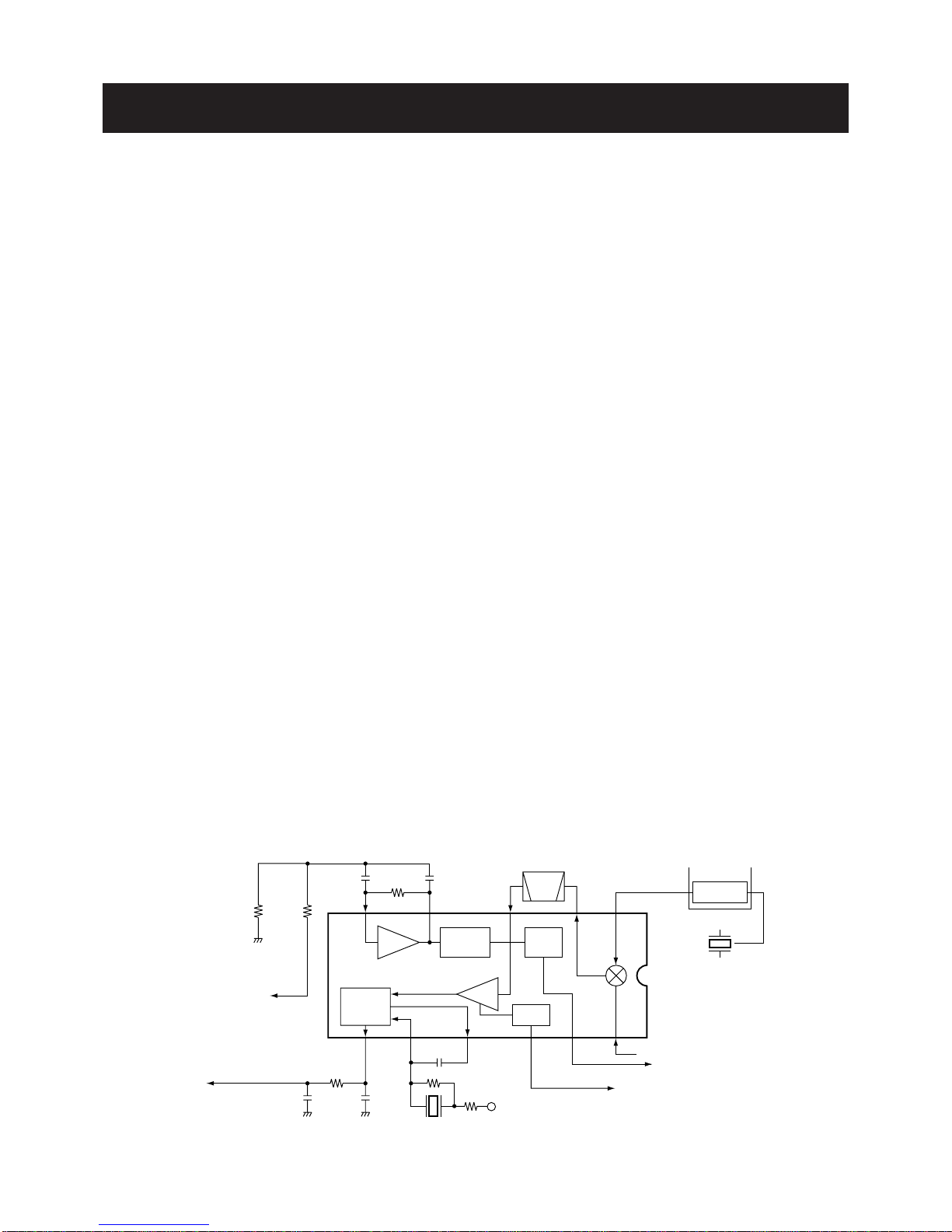
4-1-5 AF CIRCUIT
AF signals from the FM IF IC (IC2, pin 9) are applied to the
mute switch (IC4, pin 1) via the AF filter circuit (IC3b, pins 6,
7). The output signals from pin 11 are applied to the AF
power amplifier (IC5, pin 4) after being passed through the
[VOL] control (R143).
The applied AF signals are amplified at the AF power ampli-
fier circuit (IC5, pin 4) to obtain the specified audio level. The
amplified AF signals, output from pin 10, are applied to the
internal speaker (SP1) as the “SP” signal via the [SP] jack
when no plug is connected to the jack.
4-1-6 SQUELCH CIRCUIT
Asquelch circuit cuts out AF signals when no RF signals are
received. By detecting noise components in the AF signals,
the squelch switches the AF mute switch.
Aportion of the AF signals from the FM IF IC (IC2, pin 9) are
applied to the active filter section (IC2, pin 8) where noise
components are amplified and detected with an internal
noise detector.
The active filter section amplifies noise components. The fil-
tered signals are rectified at the noise detector section and
converted into “NOIS” (pulse type) signals at the noise com-
parator section. The “NOIS” signal is applied to the CPU
(IC8, pin 19).
The CPU detects the receiving signal strength from the
number of the pulses, and outputs an “RMUT” signal from
pin 49. This signal controls the mute switch (IC4) to cut the
AF signal line.
4-1-7 WIDE AND NARROW SWITCHING CIRCUIT
The “NWC” signal from the CPU (IC8, pin 38) is applied to
the Q41. Q41 is switched ON or OFF by the signal. Q41 con-
trols IC2’s detector output to same level both wide band
mode and narrow band mode.
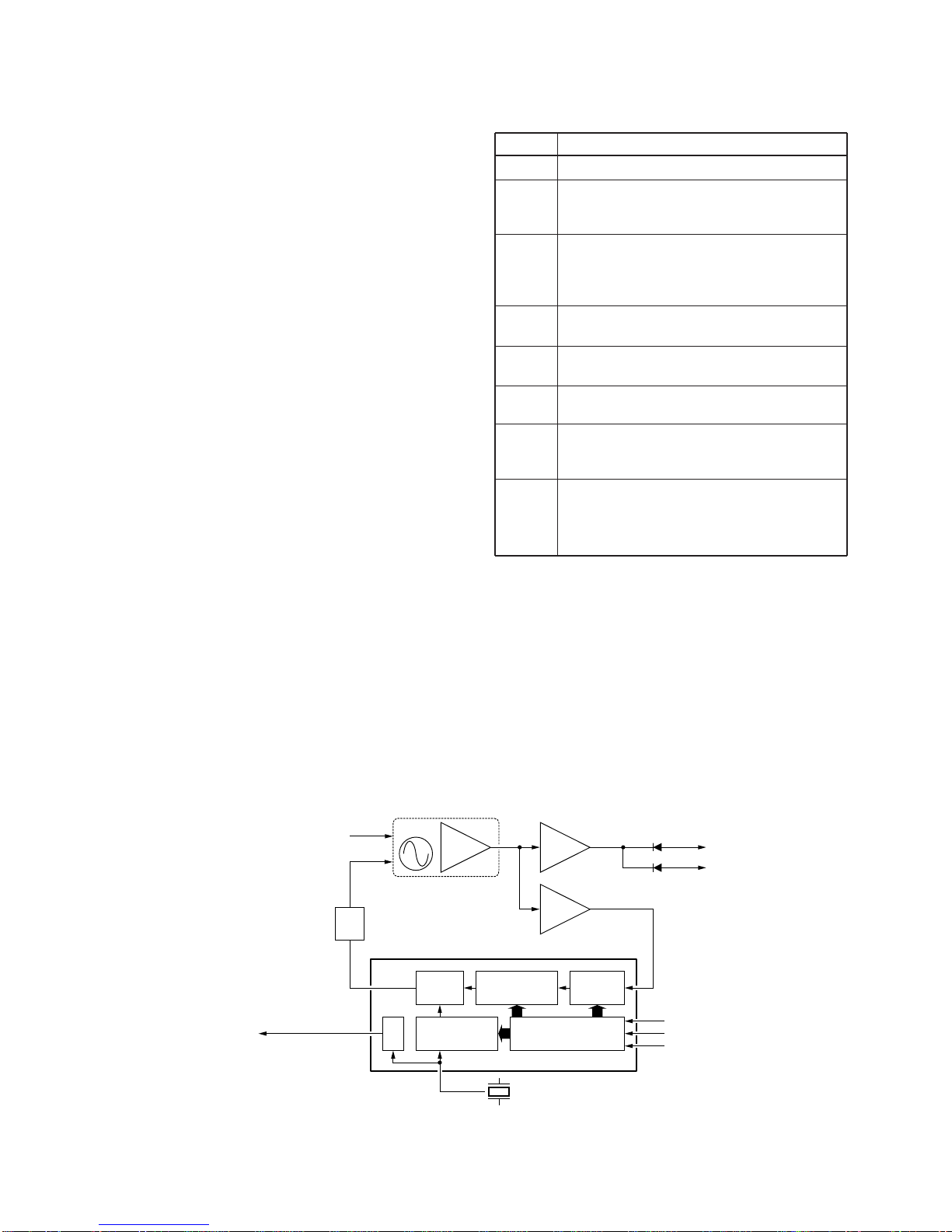
4-2 TRANSMITTER CIRCUITS
4-2-1 MICROPHONE AMPLIFIER CIRCUIT
The microphone amplifier circuit amplifies audio signals with
+6 dB/octave pre-emphasis characteristics from the micro-
phone to a level needed for the modulation circuit.
The AF signals from the microphone are applied to the
microphone amplifier circuit (IC3c, pin 10). The amplifiedAF
signals are passed through the low-pass filter circuit (IC3d,
pins 13, 14) via the mute switch (IC4, pins 4, 3, 2). The fil-
tered AF signals are applied to the modulator circuit after
being passed through the mute switch (IC4, pins 9, 8).
4-2-2 MODULATION CIRCUIT
The modulation circuit modulates the VCO oscillating signal
(RF signal) using the microphone audio signal.
The audio signals from the D/A convertor (IC10, pin 22)
change the reactance of a diode (D6) to modulate an oscil-
lated signal at the VCO circuit (Q7, Q8). The oscillated sig-
nal is amplified at the buffer-amplifiers (Q4, Q6), then
applied to the T/R switching circuit (D3, D4).
4-2-3 DRIVE/POWER AMPLIFIER CIRCUITS
The signal from the VCO circuit passes through the T/R
switching circuit (D3) and is amplified at the buffer (Q3),
drive (Q2) and power amplifier (Q1) to obtain 5 W of RF
power (at 7.2 V DC). The amplified signal passes through
the antenna switching circuit (D1), and low-pass filter and is
then applied to the antenna connector.
The bias current of the drive (Q2) and the power amplifier
(Q1) is controlled by the APC circuit.
4-2-5 APC CIRCUIT
The APC circuit (IC3a, Q37) protects the drive and the
power amplifiers from excessive current drive, and selects
HIGH or LOW output power.