IDT VersaClock 6 5P49V69 Series User manual
USER GUIDE
REVISION 12/03/15 1 ©2015 Integrated Device Technology, Inc.
VersaClock®6 - 5P49V69xx Family Programmer
Board
Introduction
The VersaClock6 - 5P49V69xx family programmer board is made to ease the programming of blank 5P49V69xx parts. With the
on-board USB interface, IDT Timing Commander™ GUI can be used to communicate with the VersaClock5 family of devices in
the socket for configuration and programming. The family of VersaClock 6 devices includes the following part numbers:
5P49V6901, 5P49V6913, 5P49V6914.
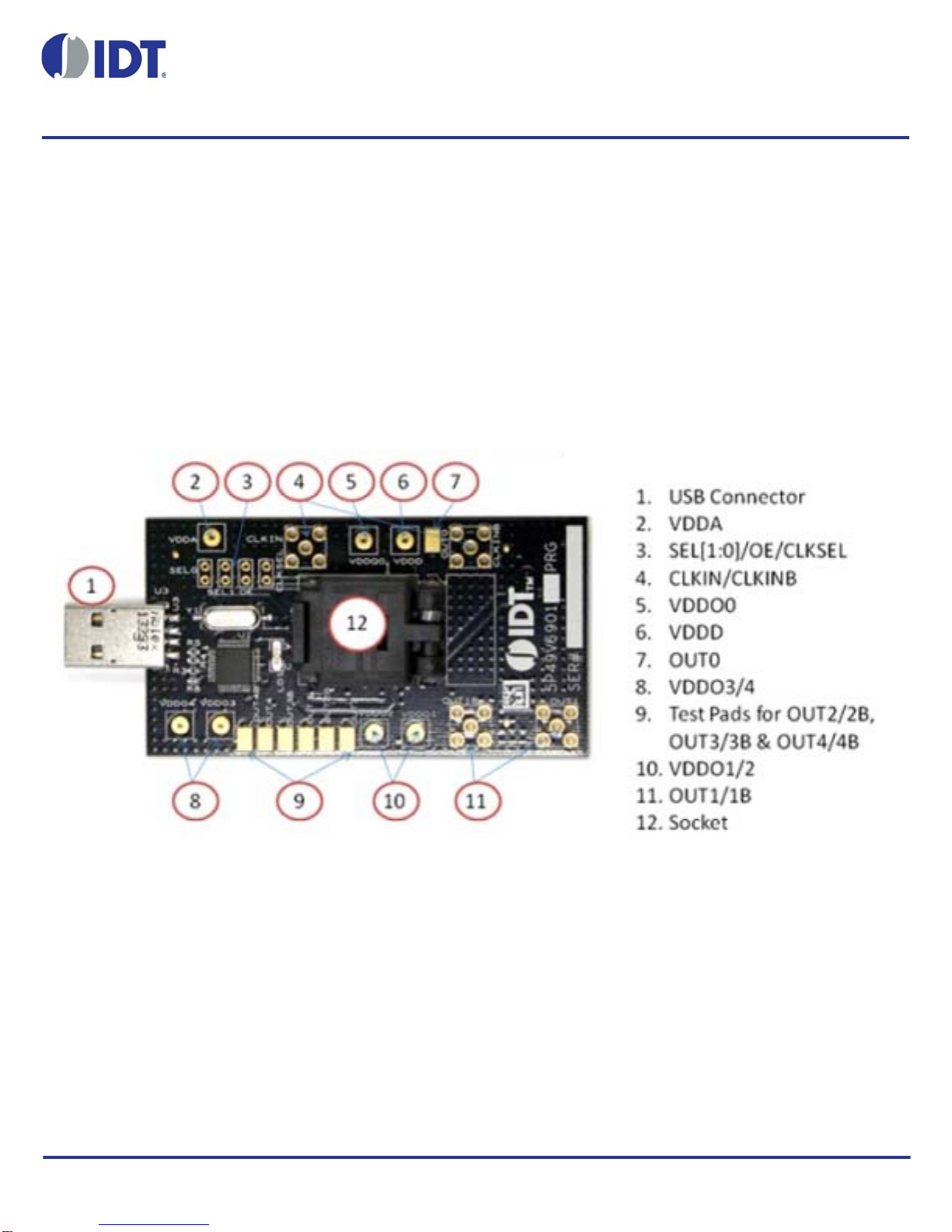
Board Overview
As shown the in the following diagram, all necessary components and connections are available to test the functionality of the
configuration after the device is programmed. By installing R14 on the back of the board with a 100Kresistor, the device will
be powering up in hardware select mode, in which SEL1 and SEL0 pins can be used to switch among 4 configurations that the
device supports.
Figure 1. Programmer Board Overview (socket closed)
Placing a Blank Chip in the Socket
When socket is open, identify the position of Pin 1 as shown in Figure 2. Align the dot of the blank device with the round dent
engraved on the corner of the socket as pointed. After placing the blank device, secure the socket cover.
REVISION 12/03/15 2
VERSACLOCK®6-5P49V69xxFamilyProgrammerBoard
Figure 2. Programmer Board Overview (socket open)
Programming Steps
1. Place a blank part in the socket–Refer to Figure 2 above. With socket opened, identify pin 1 position and place a blank part
accordingly. Close the socket and secure the socket lid.
2. Plug the board into USB port –USB port provides power to the board as well as a communication channel between GUI and
the device.
3. Start Timing Commander GUI–Launch the Timing Commander GUI software. Load the proper personality file.
4. Start a new settings file or open a pre-optimized configuration file.
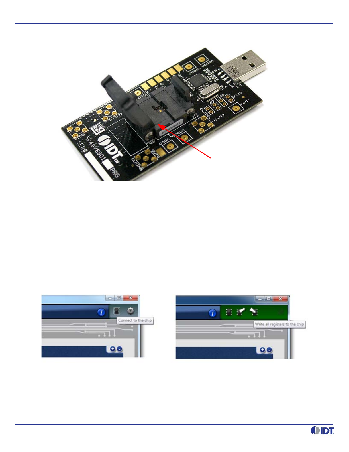
5. Connect to the board–Click on the chip symbol on the top-right corner of the GUI window, as shown in Figure 3 below (left).
A rectangular area in green will display (right).
Figure 3. Connecting to the chip: Left: click on the chip symbol to make the connection; Right: A green area
appears if I2C communication is established.
6. Execute “Write All” command–Double check the setting file that is open in GUI window and make sure everything is correct.
Then click on “Write-All” symbol in the green area (See Figure 3 above, right). This is a step that must be executed before OTP
programming of the device.
7. Click on OTP button in the GUI–On lower left portion of GUI window, there is a button called OTP (Figure 4: left). Click this
button to open OTP Programming dialogue window (Figure 4: right).
Pin 1

REVISION 12/03/15 3
VERSACLOCK®6-5P49V69xxFamilyProgrammerBoard
Figure 4. OTP Dialogue Window
In OTP dialogue window, there is a box in front of each configuration. Check the box for the configuration(s) that you want to
program. One or more configurations can be selected at the same time. If All is checked, all 4 configuration will be programmed.
After intended configuration(s) is selected, then programming the device is only one click away – click on the blue “Burn” button
will launch the programming. If one or more of the target configurations have already been burned, there will be a warning.
Once done, a completion message will pop out which indicates a successful programming:
Figure 5. Message for Successful Programming
Important: Burning irreversibly converts ones to zeroes; it is possible to go back and burn an unburned bit or bits to zero; zeroes
cannot be restored to ones. This allows revision of a burn under limited circumstances.
Loading from OTP
For loading one or more configurations from a burned part into the VC6 GUI (“load OTP”) follow these steps: Before reading back
cycle the power on the part and set the input crystal and/or clock frequencies in the GUI to those in the original configuration(s).
This must be done manually because there is no way to store this information on the part itself. If there is more than one
configuration, this step must be repeated for each one.
Connect to the part. The “OTP” button becomes enabled. The “Active” and “Configuration” indicator lights will be displayed (see
Figure 6 below), and be illuminated or dark as appropriate. The green “Active” light means that the “OTP Burned” bit (R0[7]) has
been burned. The red “Configuration” lights are illuminated as appropriate: if on, that configuration in the OTP has been burned.
Click the “OTP” button. In the OTP dialog, check the boxes of the configurations to be loaded. If you check a box corresponding
to an unburned configuration, there will be a warning (see Figure 7 below).If there are four configurations, there is an “All”
checkbox for convenience (see Figure 8 below). Click “Load”.

REVISION 12/03/15 4
VERSACLOCK®6-5P49V69xxFamilyProgrammerBoard
Figure 6. Indicator Lights
Figure 7. Unburned Configuration Warning
Figure 8. OTP “All” Checkbox

REVISION 12/03/15 5
VERSACLOCK®6-5P49V69xxFamilyProgrammerBoard
In-System VersaClock 6 OTP Non-Volatile Programming via I2C
The procedure below enables the user to calibrate the device to a proper VCO band that will guarantee functionality over the full
temperature range of the device. That band will then be programmed into the OTP. Certain conditions are required to properly
program the device.
1. Conditions: Ambient temperature 25°C, 3.3V. For any other conditions, contact IDT.
2. Procedure:
a.Power-up the device
b.Write all relevant bits to the device to program PLL, FOD and output types
c. Provide a reference clock to the IC corresponding to the configuration.
d.Specific bits need to be set:
• Set VCO Monitoring in address x1D, bit[1] to “0”
• Set “AFC Enable” bit in address x16, bit[3] to “0”
• Set Test mode bit in register 0x11 (bit[5]) to “0”
e.Perform VCO Calibration:
• Toggle bit[7] in 0x1C by writing the bit to 0 then 1 and then back to 0. Final state of the bit should be 0.
• Wait 100 ms
• Read band in I2C register 0x99 bit[7:3]
(read only register located in the factory programmable section of the RAM)
• The value readfrom register 0x99 has to be different from 0 or 23. If this isnot the case then repeat the Calibrationstep.
• Write the content of the I2C register 0x99 bit[7:3] to the bits bit[4:0] into register 0x11.
f. Programming the OTP
Before programming the OTP, change Test mode bit in register 0x11 (bit[5]) to “1” to force the chip to run the band number written
previously in bits[4:0].
Now program the OTP by following the steps on page 5 of the VersaClock 6 Family Register Descriptions and Programming
Guide.

REVISION 12/03/15 6
VERSACLOCK®6-5P49V69xxFamilyProgrammerBoard
VersaClock 6 Volatile Programming via I2C
The procedure below enables the user to calibrate the device to a proper VCO band that will guarantee functionality over the full
temperature range of the device. Certain conditions are required to properly calibrate the VCO.
1. Conditions: Ambient temperature 25°C, 3.3V. For any other conditions, contact IDT.
2. Procedure:
a.Power-up the device
b.Write all relevant bits to the device to program PLL, FOD and output types
c. Provide a reference clock to the IC corresponding to the configuration writteninpointb.
d.Specific bits need to be set:
• Set VCO Monitoring in address x1D, bit[1] to “0”
• Set Test mode bit in register 0x11 (bit[5]) to “0”
e.Perform VCO Calibration:
f. Toggle bit[7] in 0x1C by writing the bit to 0 then 1 and then back to 0. Final state of the bit should be 0.
• Wait 100 ms

REVISION 12/03/15 7
VERSACLOCK®6-5P49V69xxFamilyProgrammerBoard
Programmed Device Testing
As indicated in the Board Overview section, the programmed device can be verified with this same board. To verify, complete the
following:
•Install R14 (100K) and then power up to latch the board in hardware selection mode
•Pull-up or pull-down SEL1 and SEL0 pins to proper levels to match the specific configuration for verification
•Supply VDDA, VDDD and VDDO0~4
•Supply a reference signal via CLKIN/CLKINB (needed to populate C20 and C22) or a Crystal (X1) needs to placed, if not
populated in the 3.2x2.5mm package.
•In order to probe the output(s) of interest the following components need to be placed:
1) R15 and C15 need to be populated to measure OUT0.
2) R17, R18 and J2 to measure OUT1.
3) R20, R21 and J3 to measure OUT1B. R19 s required only when measuring OUT1B and OUT1 in LVDS mode.
4) R26, R27 to measure OUT 2.
5) R30, R31 to measure OUT2B. R29 is only required when measuring OUT2B and OUT2 in LVDS mode.
6) R34, R35 to measure OUT 3.
7) R37, R39 to measure OUT3B. R36 is only required when measuring OUT3 and OUT3B in LVDS mode.
8) R41, R42 to measure OUT4.
9) R44, R45 to measure OUT4B. R43 is only required when measuring OUT4B and OUT4 in LVDS mode.
The recommended values depends on which driver output has been selected – LVDS, LVPECL, HCSL or LVCMOS:
•LVCMOS requires 33resistor termination in series.
•LVDS requires 0resistor in series and 100in parallel between the 2 differential outputs.
•LVPECL requires 0resistor in series and 180to ground for each differential signal.
•HCSL requires 33resistor in series and 50to ground for each differential signal.
Please refer to the board schematics on the following pages of this document.

REVISION 12/03/15 8
VERSACLOCK®6-5P49V69xxFamilyProgrammerBoard
5
5
4
4
3
3
2
2
1
1
D D
C C
B B
A A
3mm
L
L
2.0 oz
Copper
L = 5mm is more
than enough
PCB Copper Decal
Recommandations for LM317LD
SO-8
XTOUT
3V3_USB
3V3_USB
XTIN
VCC2232
3V3_USB
VCC2232
USB_5V
VCC2232_3V
USB_5V
SEL1_SDA
SEL0_SCL
USB_PWR
Title
Size Document Number Rev
Date: Sheet of
<Doc> <RevCod
e
<Title>
B
12Monday, January 27, 2014
Title
Size Document Number Rev
Date: Sheet of
<Doc> <RevCod
e
<Title>
B
12Monday, January 27, 2014
Title
Size Document Number Rev
Date: Sheet of
<Doc> <RevCod
e
<Title>
B
12Monday, January 27, 2014
C7
33pf
C6
0.047uF
L1
600 ohm 500mA
R2
470
C45
0.1uF
R59 402_1%
R7 0
C5
0.1uF
R4
27
C2 0.1uF
U3
USB_A
VBUS 1
D+ 3
GND 4
D- 2
R5 1.5K
U1
ft2232_chip
EESK
1
EEDATA
2
VCC 3
RESET#
4
RSTOUT#
5
3V3OUT
6
USBDP
7
USBDM
8
GND
9
SI/WUA 10
GPIOH3 11
GPIOH2 12
GPIOH1 13
VCCIOA 14
GPIOH0 15
GPIOL3 16
GPIOL2 17
GND
18
GPIOL1 19
GPIOL0 20
TMS/CS 21
TDO/DI 22
TDI/DO 23
TCK/SK 24
GND
25
SI/WUB 26
UNUSED11 27
UNUSED10 28
UNUSED9 29
UNUSED8 30
VCCIOB 31
UNUSED7 32
UNUSED6 33
GND
34
UNUSED5 35
UNUSED4 36
UNUSED3 37
UNUSED2 38
UNUSED1 39
UNUSED0 40
PWREN# 41
VCC 42
XTIN
43
XTOUT
44
AGND
45 AVCC 46
TEST
47
EECS
48
R9
10K
R3
27
C3 0.1uF
R10 10K C46
10uF
C1 10nF
R1
680
R6 0
C8
33pf
C4
10uF
LD1
Green
Y1
6MHz
12
U5
LM317LBD
VIN
1
VOUT_2
2
VOUT_3
3
Adjust
4
NC_8 8
VOUT_7 7
VOUT_6 6
NC_5 5
R58
243_1%
R8 10K

REVISION 12/03/15 9
VERSACLOCK®6-5P49V69xxFamilyProgrammerBoard
5
5
4
4
3
3
2
2
1
1
D D
C C
B B
A A
SD/OE
VDDD
VDDQ0
VDDO1
VDDO3
VDDO4
CLKSEL
VDDA
VDDO2
SEL1/SDA
SEL0/SCL
VDDD
VDDD
VDDD
VDDD
VDDD
VDDD
VDDD
VDDD
VDDD
SEL1_SDA
SEL0_SCL
USB_PWR
USB_PWR
USB_PWR
USB_PWR
USB_PWR
USB_PWRUSB_PWR
Title
Size Document Number Rev
Date: Sheet of
<Doc> <RevCode>
<Title>
C
22Friday, January 24, 2014
Title
Size Document Number Rev
Date: Sheet of
<Doc> <RevCode>
<Title>
C
22Friday, January 24, 2014
Title
Size Document Number Rev
Date: Sheet of
<Doc> <RevCode>
<Title>
C
22Friday, January 24, 2014
TP2
R38
10(np)
R18
180(np), 49.9(np)
R24
1k(np)
R23
49.9(np)
R41
0(np), 33(np)
R50
0 (np)
C33
10u(np)
C23
2p(np)
R17
0(np), 33(np)
R12
0
C28
10u(np)
R30
0(np), 33(np)
C30
2p(np)
C16
10u(np)
C13
10u(np)
R39
180(np), 49.9(np)
TP6
OUT2
R28
1k(np)
R43
100(np)
C34
0.1u(np)
R27
180(np), 49.9(np)
U2
IDT5P49V5901
CLKIN
1
CLKINB
2
XOUT
3
XIN/REF
4
VDDA
5
CLKSEL
6
SD/OE
7
SEL1/SDA
8
SEL0/SCL
9
VDDO4
10
OUT4
11
OUT4B
12
OUT3B 13
OUT3 14
VDDO3 15
OUT2B 16
OUT2 17
VDDO2 18
OUT1B 19
OUT1 20
VDDO1 21
VDDD 22
VDDO0 23
OUT0_SELB_I2C 24
e_PAD 25
R32
49.9(np)
JP2
OE
R16
0
J4
TP12
OUT4B
R29
100(np)
TP4
OUT0_SELB_I2C
C17
0.1u(np)
R25
100(np)
C29
0.1u(np)
R37
0(np), 33(np)
X1
25MHz(np)
1 3
2
4
R49
4.7k
C24
10p(np)
C18
2p(np)
C26
2p(np)
JP3
SEL1
C9
10u(np)
R26
0(np), 33(np)
C31
2p(np)
J5
C11
0.1u(np)
R13
0
R45
180(np), 49.9(np)
TP8
OUT3
TP3
R33
1k(np)
R35
180(np), 49.9(np)
C35
10u(np)
C20
0.1u(np)
TP5
JP4
SEL0
R51
0
C25
10p(np)
TP7
OUT2B
R21
180(np), 49.9(np)
J3
C19
2p(np)
R44
0(np), 33(np)
TP1
C10
0.1u(np)
R47
0 (np)
C21
2p(np)
R22
1k(np)
R34
0(np), 33(np)
R15
20(np)
TP11
OUT4
C32
0.1u(np)
C27
2p(np)
TP9
R36
100(np)
C12
10u(np)
J2
R20
0(np), 33(np)
R46
4.7k
TP14
C22
0.1u(np)
R48
0
R42
180(np), 49.9(np)
C15
5p(np)
R14
100k(np)
TP13
C14
0.1u(np)
TP10
OUT3B
R31
180(np), 49.9(np)
R40
0
R19
100(np)
R11
0
JP1
CLKSEL

DISCLAIMER Integrated Device Technology, Inc. (IDT) and its subsidiaries reserve the right to modify the products and/or specifications described herein at any time and at IDT’s sole discretion. All information in this document,
including descriptions of product features and performance, is subject to change without notice. Performance specifications and the operating parameters of the described products are determined in the independent state and are not
guaranteed to perform the same way when installed in customer products. The information contained herein is provided without representation or warranty of any kind, whether express or implied, including, but not limited to, the
suitability of IDT’s products for any particular purpose, an implied warranty of merchantability, or non-infringement of the intellectual property rights of others. This document is presented only as a guide and does not convey any
license under intellectual property rights of IDT or any third parties.
IDT’s products are not intended for use in applications involving extreme environmental conditions or in life support systems or similar devices where the failure or malfunction of an IDT product can be reasonably expected to signifi-
cantly affect the health or safety of users. Anyone using an IDT product in such a manner does so at their own risk, absent an express, written agreement by IDT.
Integrated Device Technology, IDT and the IDT logo are registered trademarks of IDT. Product specification subject to change without notice. Other trademarks and service marks used herein, including protected names, logos and
designs, are the property of IDT or their respective third party owners.
Copyright 2015. All rights reserved.
Corporate Headquarters
6024 Silver Creek Valley Road
San Jose, CA 95138 USA
Sales
1-800-345-7015 or
408-284-8200
Fax: 408-284-2775
www.IDT.com
Support
www.idt.com/go/support
VERSACLOCK®6 - 5P49V69xx Family Programmer Board
This manual suits for next models
3
Table of contents
Other IDT Motherboard manuals

IDT
IDT VersaClock 5 User manual

IDT
IDT 82V3911 User manual

IDT
IDT EB-LOGAN-23 User manual

IDT
IDT 82P33714 User manual

IDT
IDT ADC1410S Series User manual

IDT
IDT ZSSC4151 User manual

IDT
IDT PhiClock 9FGV1001 User manual

IDT
IDT 89EBPES12N3 User manual

IDT
IDT 89EB-LOGAN-19 User manual

IDT
IDT VersaClock 3S User manual

IDT
IDT Tsi382 LQFP User manual

IDT
IDT EB8T5A Eval Board User manual

IDT
IDT EB4T4 Eval Board User manual

IDT
IDT VersaClock 3S User manual

IDT
IDT 8A34 Series User manual

IDT
IDT Tsi340-RDK1 User manual

IDT
IDT 5P49V5907 Manual

IDT
IDT ZMOD4410 User manual

IDT
IDT 89EBPES48H12 User manual

IDT
IDT P9241-G-EVK User manual


