JEOL JEM-1200EX User manual

INSTRUCTIONS
JEM - I 200EX
ELECTRON MICROSCOPE
dEOL.
No. IEM1200EX-2
(EM157012)
JEOL LTD. / 19*il
F5(Afke--cLf")
Tokyo Japan
E(eetelp.„,
8309081 HP

To the user:
4
This instruction manual covers the operating
procedures for the basic JEM-1200EX Electron Mi-
4
croscope. That is to say, if the instrument delivered
6
4
1
to your institution has been modified in any way to
4
satisfy your specific research requirements, certain
aspects of the manual will require certain (minor)
amendments. If in any doubt, please contact your
4
nearest JEOL Service Center.
1
1200EX-1

1
AMENDMENTS TO INSTRUCTION MANUAL
JEM-1200EX
No. CI1EM1200EX-2
(EM157012)
The instrument has undergone certain modifications in order to improve performance and facilitate
operation. Please, therefore, note the following changes and correct your manual accordingly. We regret any
inconvenience caused.
1.
Although the parts listed below are optional accessories, they are described as standard items in this manual
for the sake of convenience. They are: anti-contamination device, refrigerant funnel, refrigerant drainer,
beam stopper, specimen grid case, hexagonal screwdrivers, activated alumina trap and tweezers.
2.
Some controls on control panel LI have been changed as follows:
Ll- C)
:
ROOM LIGHT:
Used for turning on/off the room light.
Ll- C)
:
BRIGHT ZOOM:
For the zoom circuit (see Subsect. 5.2.11q).
Ll- C)
:
BRIGHT 16X:
When this button is switched on, the button lamp lights up and the 2nd con-
denser lens current range, variable by the BRIGHTNESS knob (control panel
L1), enlarges 16 times.
3.
To set the magnification when the MAG2 button (control panel R1) is depressed (this magnification is called
"basic magnification") at 5,000 times, refer to Subsect. 5.2.11r.
4.
The name of the knobs, IW ADJ, on control panel R2 has been changed to "IMAGE WOBBLER ADJ".
5.
The names of the keys, C/R,
1
and
on the keyboard have been changed to "RETURN", "<—" and "—>"
respectively.
6.
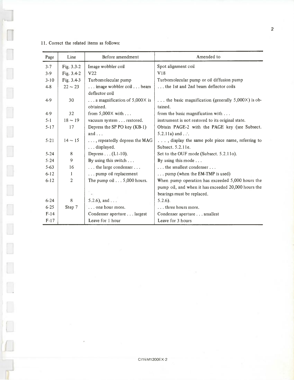
Change Steps 8 and 9 in Subsect. 6.1.2 as follows:
Step 8: Depress the GUN AIR button (L2-4). Air is admitted into the anode chamber.
Step 9: Make sure that the PI2 value (indicated on PAGE-1) has increased to 250, then turn the LIFT switch
(L2-1) to ON.
7.
Change Steps 2 and 3 in Subsect. 6.7.7b as follows:
Step 2: Make sure the electron gun has not been lifted and camera chamber door is closed.
Step 3: Switch off the COL AIR button (L2-5).
8.
In Subsect. 6.8, add another step, Step 19, after Step 18.
Step 19: Make the objective lens pole piece name displayed on PAGE-1 coincide with the name of the pole
piece being installed in the objective lens (see Subsect. 5.2.11e).
9.
The aperture disk and aperture holder of the Wehnelt assembly have been removed.
10.
Two types of objective lens aperture, 20-50-80 bunO aperture for the SHP pole piece and 50-100-150 linicb
aperture for the SAP pole piece, have been provided.
8309081

11. Correct the related items as follows:
Page
Line
Before amendment
Amended to
3-7
Fig. 3.3-2
Image wobbler coil
Spot alignment coil
3-9
Fig. 3.4-2
V22
V18
3-10
Fig. 3.4-3
Turbomolecular pump
Turbomolecular pump or oil diffusion pump
4-8
22 — 23
... image wobbler coil ... beam
deflector coil
... the
1st
and 2nd beam deflector coils
4-9
30
.. . a magnification of 5,000X is
obtained.
. . . the basic magnification (generally 5,000X) is ob-
tained.
4-9
32
from 5,000X with ...
from the basic magnification with .. .
5-1
18 — 19
vacuum system . .. restored.
instrument is not restored to its original state.
5-17
17
Depress the SP PO key (KB-1)
and ...
Obtain PAGE-2 with the PAGE key (see Subsect.
5.2.11a) and ..-.
5-21
14 — 15
. .. , repeatedly depress the MAG
. . . , display the same pole piece name, referring to
... displayed.
Subsect. 5.2.11e.
5-24
8
Depress ... (L1-10).
Set to the OUF mode (Subsect. 5.2.110).
5-24
9
By using this switch . ..
By using this mode .. .
5-63
16
. .. the large condenser .. .
. .. the smallest condenser . ..
6-12
1
... pump oil replacement
.. . pump (when the EM-TMP is used)
6-12
2
The pump oil .. . 5,000 hours.
-
When pump operation has exceeded 5,000 hours the
pump oil, and when it has exceeded 20,000 hours the
bearings must be replaced.
6-24
8
5.2.6), and . . .
5.2.6).
6-25
Step 7
.. . one hour more.
. . . three hours more.
F-14
Condenser aperture .. . largest
Condenser aperture . . . smallest
F-17
Leave for 1 hour
Leave for 3 hours
2
CI1EM1200EX-2

CONTENTS
1. GENERAL
1.1
Introduction
Fig. 1.1
Signals generated by interactions between electron beam and
specimen
Table 1.1
Main attachments
Table 1.2
Electron microscope system
1.2
Principle of electron microscope
1-
1
1-
1
1- 2
1- 3
1- 4
1.2.1
General principles
1- 4
1.2.1a
Comparison between electron microscope and optical microscope
1- 4
Table 1.3
EM and OM comparison chart
1- 4
Fig. 1.2
Comparison of image formation
1- 5
1.2.1b
Resolving power and resolution
1- 6
Fig. 1.3
Limit of resolving power
1- 6
1.2.1c
Principle of the electron lens
1- 8
Fig. 1.4
Electron trajectories
1- 8
Fig. 1.5
Trajectories of electrons emitted obliquely in a uniform
magnetic field
1- 9
Fig. 1.6
Electrons passing through a uniform magnetic field
1-10
Fig. 1.7
Types of magnetic electron lenses
1-11
Fig. 1.8
Electrons passing through magnetic lens
1-11
Fig. 1.9
Magnetic field distribution and image formation graphs
1-12
1.2.1d
Interaction between electron beam and substances
1-13
Fig. 1.10
Interaction between electrons and substances
1-13
1.2.1e
Image formation and contrast
1-14
Fig. 1.11
Scattering absorption (mass thickness) contrast
1-15
Fig. 1.12
Contrast in crystalline specimens
1-16
Fig. 1.13
Formation of equal inclination fringes
1-16
Fig. 1.14
Dynamical effect of electron waves
1-17
Fig. 1.15
Image of specimen having periodic structure
1-19
Fig. 1.16
Formation of Moire patterns by double diffraction
1-20
1.2.1f
Electron diffraction
1-21
Fig. 1.17
Electron diffraction
1-22
Fig. 1.18
Selected area electron diffraction
1-23
1.2.2
Outline of structure
1
24
1.2.2a
Electron gun
1
24
Fig. 1.19
Generation of electron beam
1
24
1.2.2b
Condenser lens
1-25
Fig. 1.20
Electron beam illumination
1 25
1.2.2c
Specimen chamber
1-26
0-1
1200EX-1

0-2
1-27
Fig. 1.21
Use of lenses and ray diagrams
1-28
1.2.2e Viewing chamber and camera chamber
1-27
1.2.2f Vacuum system
1-29
Fig. 1.22
Structure of a Gaede oil rotary pump
1-29
Fig. 1.23
Sputter-ion pump
1-30
Fig. 1.24
Turbomolecular pump
1-31
Fig. 1.25
Schematic diagram of vacuum system
1-31
1.2.2g Electrical system
1-32
Fig. 1.26
Schematic diagram of high voltage circuit
1-32
Fig. 1.27
Schematic diagram of lens circuit
1-33
Fig. 1.28
Schematic diagram of beam deflector circuit
1-33
Fig. 1.29
Schematic diagram of exposure circuit
1-34
2. SPECIFICATIONS
2.1 Performance
2- 1
2.2
Electron optical system
2- 1
2.2.1 Illuminating system
2- 1
2.2.2 Image forming system
2- 1
2.3
Specimen stage
2- 2
2.4
High resolution diffraction chamber
2- 2
2.5
Viewing chamber
2- 2
2.6 Camera chamber
2- 2
2.7 Vacuum system
2 2
2.8
Installation requirements
2 3
2.8.1 Power supply and cooling water
2- 3
2.8.2 Installation room
2- 3
2.8.3 Dimensions and weight
2- 3
2.9 Warranty
2- 3
1.2.2d Image forming lens system
3. COMPOSITION AND CONSTRUCTION
3.1 Composition
Fig. 3.1-1
3.2 Accessories
Fig. 3.2-1
Accessories (1)
Fig. 3.2-2
Accessories (2)
Fig. 3.2-3
Accessories (3)
3- 1
3- 1
3- 2
3- 2
3- 3
3- 5
3- 6
3- 6
Cross section of microscope column
3- 7
3- 8
3- 8
Composition and layout diagram
3.3
Construction of column
Fig. 3.3-1
Fig. 3.3-2
External view of column
3.4 System diagrams
Fig. 3.4-1
Vacuum system
1200EX-1

Fig. 3.4-2
Compressed air system
3- 9
Fig. 3.4-3
Cooling water system
3-10
Fig. 3.4-4
Electrical system
3-11
3.5
Location of control panels
3-12
Fig. 3.5-1
Control panels
3-12
4.
DESCRIPTION OF COLUMN AND PANEL CONTROLS
4.1 Column
4- 1
Fig. 4.1-1
Aperture assembly
4- 1
Fig. 4.1-2
Specimen selecting device
4- 2
Fig. 4.1-3
Goniometer
4- 2
Fig. 4.1-4
Pedal switches
4- 4
4.2
Control panels
4- 5
4.2.1 Control panel Ll
4- 5
Fig. 4.2-1
Control panel Ll
4- 5
4.2.2 Control panel R1
4- 8
Fig. 4.2-2
Control panel RI
4- 8
4.2.3 Control panel L2
4-11
Fig. 4.2-3
Control panel L2
4-11
4.2.4 Control panel R2
4-12
Fig. 4.2-4
Control panel R2
4-12
4.2.5 Keyboard (KB)
4-14
Fig. 4.2-5
Keyboard
4
14
4.2.6 CRT display
4-16
5.
OPERATION
5.1 Emergencies
5-
1
5 1
5- 1
5 1
5- 2
5-
2
5-
3
5-
3
5 3
5- 4
5. 4
5-
4
5
5
5- 6
5
6
5.1.1 Power suspension
5.1.2 Cooling water suspension
5.1.3 Faulty operation
5.2 Method A
5.2.1 Startup procedure
5.2.2 Film loading
5.2.2a Loading films into the dispensing magazine
Fig. 5.2-1
Loading films into the dispensing magazine
5.2.2b Inserting (or removing) the magazines into (or from) the camera chamber
Fig. 5.2-2
PAGE-1
Fig. 5.2-3
Camera chamber
Fig. 5.24
Magazine stand
Fig. 5.2-5
Magazines
Fig. 5.2-6 Writing the UNUSED number
0-3
1200EX-2

5- 7
Fig. 5.2-7 EM-SQH specimen holder box and stand
5- 7
Fig. 5.2-8
Installing the specimen exchange mount
5- 8
Fig. 5.2-9
Specimen exchange
5- 8
5- 9
Table 5.1
Accelerating voltage and related detecting current values
5- 9
Fig. 5.2-10 Accelerating voltage and spot size
5- 9
Fig. 5.2-11 Aperture assembly
5-10
Fig. 5.2-12 Specimen holder installed on the column
5-10
Fig. 5.2-13 PAGE-3
5-11
Fig. 5.2-14 Condenser lens alignment
5-13
5.2.5 Inserting the condenser lens aperture into the beam path
5-14
Fig. 5.2-15 Condenser lens aperture assembly
5-14
Fig. 5.2-16 Condenser lens aperture alignment
5-15
5.2.6 Specimen holder insertion
5-16
Fig. 5.2-17 X-tilt scale
5-16
Fig. 5.2-18 Goniometer
5-16
Fig. 5.2-19 Specimen selecting device
5-17
Fig. 5.2-20 Adjusting the field of view
5-18
5.2.7 Inserting the objective lens aperture into the beam path
5-19
Fig. 5.2-21 Caustic spot
5-19
Fig. 5.2-22 Objective lens aperture assembly
5-19
Fig. 5.2-23 Objective lens aperture alignment
5-20
5.2.8 Image observation
5-21
5-21
5.2.9 Image recording by automatic exposure
5-23
Fig. 5.2-25 Photographing area
5-23
Fig. 5.2-26 Fields allowing information to be written
5-23
Fig. 5.2-27 Binoculars
5-24
Fig. 5.2-28 Focusing with the image wobbler
5-25
Fig. 5.2-29 Optimum underfocus
5-26
Fig. 5.2-30 Exposure time
5-27
5.2.10 Film processing
5-28
Fig. 5.2-31 Removing the film from the cassette
5-28
Fig. 5.2.32 Film processing
5-29
Table 5.2
Consequence of faulty film processing
5-30
5.2.11 Keyboard operation
5-31
5-31
5.31
5-31
5-31
5-31
5.2.3 Specimen preparation
5.2.4 Electron beam generation
Fig. 5.2-24 PAGE-1
5.2.11a
PAGE
change
5.2.11b
ALIGN
display
5.2.11c Recording by printer
5.2.11d PC board check
5.2.11e Changing the name of pole piece
1200EX-2
0-4

0-5
Fig. 5.2-33 PAGE-1
5-32
5.2.11f Character writing
5-32
5.2.11g Writing the specimen name
5-33
Fig. 5.2-34 TEXT writing
5-33
5.2.11h Setting the minimum increment of accelerating voltage
5-33
5.2.11i Storing the position of the field of view in the memory
5-33
Fig. 5.2-35 PAGE-2
5-34
5.2.11j Setting the film number and number of unused films
5-34
5.2.11k Selecting the camera
5-34
5.2.11/ Setting the exposure index
(bentus
i.4-.Wif-3.
)
5-34
5.2.11m Storing the lens system condition and setting the lens system
at the stored condition
5-35a
5.2.11n Setting the through-focus series conditions
5-35a
5.2.110 Setting the amount of OUF (optimum underfocus)
5-35a
5.2.11p Setting the mode of minimum exposure operation
5-35b
5.2.11q Using the BRIGHT ZOOM system
5-35b
5.2.11r Setting the basic magnification
5-35b
5.2.11s Writing USER'S COMMENTS
5-35c
5.2.12 Shutdown procedure
5-36
5.2.13 Data printout on micrograph
5-36
Fig. 5.2-36 Data printout on micrograph
5-36
5.3 Method
B
5-37
5.3.1 CRT display
5-37
5.3.2 Column alignment
5-38
Fig. 5.3-1
Beam displacement compensating screws
5-40
5.4 Method C
5-43
5.4.1 Column alignment
5-43
Fig. 5.4-1
Filament image
5-46
5.4.2 Objective lens astigmatism correction
5-46
Fig. 5.4-2
Test hole for astigmatism correction
5-47
Fig. 5.4-3
Objective lens astigmatism
5-47
5.4.3 Focusing
5.48
Fig. 5.4-4
Focusing with the aid of the Fresnel fringe
5.49
Fig. 5.4.5
Schematic diagram showing various focus conditions
5-49
Fig. 5.4-6
Practical example of focusing
5-50
5.4.4 Image recording
5-51
5.4.4a Manual exposure
5-51
5.4.4b Continuous photography
5-51
5.4.4c Multiple exposure
5-51
5.5
Conditions for high magnification/high resolution microscopy
5-53
Fig. 5.5-1
Effect of voltage center alignment
5-53
Fig. 5.5-2
Effect of objective lens aperture insertion
5-54
Fig. 5.5-3
Effect of objective lens astigmatism
5-54
1200EX-2

Fig. 5.5-4
Effect of image drift
5 55
Fig. 5.5-5
Fresnel fringe and background structure variation
5 56
5.6
Special observations
5-57
5.6.1 Low magnification images
5-57
Fig. 5.6-1
Field limiting aperture assembly
5-58
Fig. 5.6-2
Low magnification image
5-58
5.6.2 Dark field images
5-59
Fig. 5.6-3
Comparison of bright and dark field images
5-59
5.6.3 Through-focus method
5-60
5.6.4 Minimum exposure operation (MDS)
5-61
5.7
Electron diffraction
5-62
5.7.1 Selected area electron diffraction
5-62
Fig. 5.7-1
Selected area electron diffraction
5-63
5.7.2 Microbeam electron diffraction
5-63
Fig. 5.7-2
Microbeam electron diffraction
5-64
5.7.3 High dispersion electron diffraction
5-64
Fig. 5.7-3
High dispersion electron diffraction
5-65
5.8
How to use the anticontamination device
5-66
5.8.1 Filling the refrigerant tank
5-66
Fig. 5.8-1
Pouring in liquid nitrogen refrigerant
5-66
5.8.2 Raising the refrigerant tank temperature to room temperature
5-67
Fig. 5.8-2
Draining off the refrigerant
5-67
5.9
How to use the gonicimeter
5-68
5.9.1 Specimen tilting
5-68
Fig. 5.9-1
X-tilt knob
5-68
5.9.2 Tilt axis alignment
5-69
Fig. 5.9-2
Lamp, motor, and Z control knob
5-69
Fig. 5.9-3
Axis alignment screws
5-70
5.10 Use of the objective lens pole piece SAP
5-71
Fig. 5.10-1 Objective lens pole pieces
5 71
0-6
6- 1
6- 1
6- 1
6- 2
6- 2
6- 2
6- 3
6- 3
6 4
6 4
6. MAINTENANCE
6.1
Electron gun filament replacement
6.1.1 Ascertaining the electron gun filament burnout
Fig. 6.1-1
PAGE-3
6.1.2 Admitting air into the anode chamber
Fig. 6.1-2
Flat bars
6.1.3 Filament replacement
Fig. 6.1-3
Cylinder and Wehnelt assembly
Fig. 6.1-4 Exploded view of Wehnelt assembly
6.1.4 Adjusting the Wehnelt cap
Fig. 6.1-5
Wehnelt cap adjustment
1200EX-1

6.1.5 Re-evacuating the anode chamber
6 5
6.2
Small fluorescent screen replacement
6
6
Fig. 6.2-1
Viewing chamber
6 6
Fig. 6.2-2
Small fluorescent screen replacement
6- 7
Fig. 6.2-3
Glass grounding spring
6- 7
6.3
Freon gas replenishment
6- 8
Fig. 6.3-1
Top view of high voltage generating tank
6- 8
Fig. 6.3-2
Gas control valve
6- 9
6.4 Oil rotary pump maintenance
6-10
6.4.1 Pump oil replenishment
6-10
Fig. 6.4-1
Replenishing the oil rotary pump
6-10
6.4.2 Pump oil replacement
6-10
Fig. 6.4-2
Oil rotary pump
6-11
6.4.3 Belt replacement
6-11
6.4.4 Vacuum rubber hose replacement
6-11
6.5
Turbomolecular pump
6-12
6.6
Silica gel replacement
6-12
6.7
Cleaning the column parts
6-13
6.7.1 Precautions
6-13
6.7.2 Cleaning materials, tools, etc.
6-13
6.7.3 Cleaning methods
6-14
Fig. 6.7-1
Aperture cleaning
6-15
6.7.4 Parts requiring cleaning
6-16
6.7.5 Removing and cleaning parts
6-17
6.7.5a Wehnelt assembly and anode
6-17
Fig. 6.7-2 Exploded view of Wehnelt cap
6-17
6.7.5b Aperture assemblies
6-17
Fig. 6.7-3
Aperture assemblies
6-18
Fig. 6.7.4
Aperture foil and aperture holder
6-18
6.7.6 Use of vacuum grease
6-19
Fig. 6.7-5
Use of vacuum grease
6-19
6.7.7 Breaking the column vacuum and re-evacuation
6-20
6.7.7a Admitting air into the column
6-20
6.7.7b Re-evacuating the column
6-20
6.8
Objective lens pole piece exchange
6-21
Fig. 6.8-1
ALIGN
switches
6-21
Fig. 6.8-2
Removing the beam deflector coil
6-22
Fig. 6.8-3
Specimen selecting device
6-22
Fig. 6.8-4 Removing the objective lens pole piece
6-23
Fig. 6.8-5
Objective lens pole piece
6-24
6.9
Baking out the column
6-25
Fig. 6.9-1
Lens cooling water valve
6-25
6.10 Troubleshooting
6-26
0-7
1200EX-2

[FLOWCHARTS]
Startup
F 1
Shutdown
F- 1
Routine operation (method C)
F- 2
Finding electron beam
F- 5
Film loading
F- 7
Manual exposure
F- 8
Low magnification images
F 9
Dark field images
F 10
Through-focus method
F 11
Minimum exposure operation (MDS)
F 12
Selected area electron diffraction
F 13
Microbeam electron diffraction
F 14
High dispersion electron diffraction
F 15
Electron gun filament replacement
F-16
Baking out the column
F-17
[ATTACHMENTS]
0-8
1200EX-1

1. GENERAL

Incident electrons
X-rays
Secondary electrons
Bac kscattered electrons
Transmitted electrons
r
1-1
1. GENERAL
1
.1
Introduction
""
."4""4""4
"
.""'"h."4..d"4“.."1..""
"
WM
"
P"
"
P"h
"
P."""4
"'
"
.....
.....
...... ......
"
"'
"
'"
P"
' ......
4
"
""linli".""q
"'
"4"""
"'
The JEM-1200EX is a versatile state-of-the-art high resolution electron microscope that can function
either as a combined electron microscope or an analytical electron microscope. When used in conjunction with a
scanning attachment and analytical facilities, it functions as a combined electron microscope or analytical elec-
tron microscope, and fully exhibits its capacity as a composite instrument or an analytical instrument, providing
various useful information on the specimen.
With a view to obtaining accurate information from the specimen, special attention has been paid to
improvement of the specimen environment. The dry pumping system and minimum electron dose system are
built-in to achieve this purpose. It goes without saying that various new design concepts are incorporated in the
optical system. The advanced imaging-lens system minimizes image rotation due to magnification change, curtail-
ment of field of view, and off-axial aberration.
Through keyboard operation, the optical system can be freely controlled and a specific condition can be
stored in memory and read out. Operating condition data can also be displayed on CRT and part of it printed on
film. Write-in of user's comments and storing them in memory are also possible through keyboard operation. The
troublesome alignment procedure has been greatly simplified because axial alignment procedure is displayed step
by step on CRT and the lens excitation conditions required for operation are automatically set.
These outstanding features make the JEM-1200EX the most advanced total optimum performance
system.
Fig. 1.1 Signals generated by interactions between electron beam and specimen
1200EX-1

Abbreviated
designation
Full designation
Description
Permits direct imaging of crystalline specimens with
atomic-level resolution, examination of lattice de-
fects, etc.
This attachment permits high resolution secondary
electron images and transmission scanning images to
be obtained simultaneously. The field of its use is
widened when various detectors or signal processors
are used in conjunction.
This spectrometer permits simultaneous elemental
analysis of a micro-area by highly efficient X-ray de-
tection.
This high resolution electron energy analyzer per-
mits elemental analysis in a micro-area of the speci-
men (especially effective for light element analysis)
as well as analysis of its chemical state.
Provides transmission electron diffraction patterns
in the case of ordinary specimens and reflection
electron diffraction patterns in the case of bulk
specimens. The High Resolution Electron Diffrac-
tion Hot Stage, the High Resolution Electron Dif-
fraction Cold Stage and AND Charge Neutralizer are
also available.
This device permits observation of transmitted elec-
tron images of magnetic materials and magnetic
domains free from lens field influence.
Used in conjunction with ASID, this unit provides
STEM mode dark field images with a comparatively
low electron beam current. Effective for observing
unstained biological specimens.
Camera chamber evacuation time is shortened when
films are dried in the desiccator prior to putting
them in the electron microscope camera chamber.
TEG
DSC
EDS
ASEA
AD
AMG
DFI
ASID
Top entry goniometer
Scanning image observation device
Energy dispersive X-ray spectrometer
Electron energy analyzer
High resolution electron diffraction
stage
Magnetic material observation
device
Dark field imaging device
Film desiccator
The main attachments and possible combinations are described in the following tables. For details of at-
tachments not listed, refer to the relevant specifications and catalogues.
Table 1.1 Main attachments
1-2
1200EX-1

JEM-1200EX
ASID
EDS
ASEA
MPA
CEM
SEM
AEM
i
..-
AEM
i
AEM
•
AEM
.
•
Abbreviated
designation
FLC
LBG
MPA
Full designation
Description
For independent control of the lens excitation cur-
rent which is usually preset. The memory unit of
the instrument can store in the memory the value
and reproduce it.
Brightness 5 —10 times that of conventional electron
guns is obtained by use of the LaB
6
cathode.
Measures precipitate distribution, particle distribu-
tion, particle diameter and particle area from the
scanning image.
Free lens control unit
LaB
6
cathode electron gun
Micro-particle analyzer
Table 1.2 Electron microscope system
AEM: Analytical electron microscope
CEM: Conventional electron microscope
SEM: Scanning electron microscope
1-3
1200EX-1

1-4
1.2
Principle of electron microscope .,.
1 lllllll 1111111111/1111.111111
1
I lll 11111h/01111 llllllllllll .11111/
Electron microscopes are widely used today and can be effectively handled without any knowledge of
the principle involved. The JEM electron microscope, being fully automated and simple to use, is no exception.
Thus, high performance is assured for every user, regardless of his level of skill. Even so, a rudimentary know-
ledge of how a microscope works, its structure, etc. is a distinct advantage. What follows is an attempt to fill this
need in a simple, concise fashion. Accordingly, if the user is familiar with the basic principles of electron optics
and image formation, he may proceed to Chapter 2.
1.2.1
General principles
1.2.1a Comparison between electron microscope and optical microscope
Fundamentally and functionally, electron microscopes (EM) and optical microscopes (OM) are identi-
cal. That is, both types of microscope serve to magnify minute objects normally invisible to the naked eye.
The basic difference between the two, however, is that an electron microscope uses an electron beam as a
specimen illuminating medium whereas an optical microscope uses a light beam (including ultraviolet rays)
for this purpose. Table 1.3 lists the main differences between the EM and OM.
Table 1.3 EM and OM comparison chart
Electron microscope
Optical microscope
Illuminating beam
Electron beam
Light beam
Wavelength
0.0086 nm (20kV)
750 nm (visible)
— 0.0025 nm (200kV)
— 200 nm (ultraviolet)
Medium
Vacuum
Atmosphere
Lens
Electron lens
Optical lens
(magnetic or electrostatic)
(glass)
Aperture angle
— 35' —
— 70
°
Resolving power
Point to point: 0.35 nm,
lattice: 0.14 nm
Visible: 200 nm,
ultraviolet: 100 nm
Magnification
100 X — 1,000,000 X
10X — 2,000X
(continuously variable)
(lens exchange)
Focusing
Electrically
Mechanically
Contrast
Scattering absorption,
diffraction, phase
Absorption, reflection
1 200E X-1

Illuminating source (lamp)
Illuminating source (electron gun)
CW 1
Objective lens aperture
Field limiting aperture
Intermediate lens
Projector lens
Fluorescent screen
Condenser lens
Specimen
Objective lens
Eyepiece
Naked eye
Since the illuminating beam of an electron microscope is an electron beam and the medium is vacuous,
there are certain limitations. However, by effectively using a wealth of attachments, many advantages can be
realized. This is especially true when the microcope combines scanning image microscopy, electron diffrac-
tion and X-ray analysis. Basically, component terminology of an electron microscope is similar to that of an
optical microscope (shown in Fig. 1.2).
1-5
[Optical microcope image]
[Electron microscope image]
[Electron diffraction pattern]
Fig. 1.2 Comparison of image formation
1200EX-1

Vd
2
sp
h+d
2
diff
d
sp
h
(Spherical aberration)
ddiff
(Diffraction aberration)
1.2.1b Resolving power and resolution
Image quality is usually shown by "resolving power" which is defined as the shortest distance between
two points (or two lines) which can be recognized as two different images. However, this term has two differ-
ent meanings: the resolving power of the instrument and the resolution of the micrograph. It is important
that this difference be thoroughly understood.
In the case of the optical microscope, the resolving power,
d,
is determined by diffraction aberration
as follows:
Spherical aberration and chromatic aberration can be removed almost completely;
061X
061X
µ
mita
NA
where
X: Wavelength of light
a:
Aperture angle
: Refractive index of the object space
NA:
Numerical aperture
On the other hand, electron microscopes are influenced by spherical aberration, which cannot be ef-
fectively corrected at present. Therefore, the electron beam near the axis must be utilized and the resolving
power of the electron microscope determined by a combination of spherical aberration and diffraction aberra-
tion as illustrated in Fig. 1.3. 0. Scherzer has calculated the limit of resolving power
d
m
i
n
and its objective
lens aperture angle
aopt:
d
m
i
n
= 0.43 4/ X
3
C
s
(2)
1-6
(1)
d
m
in
aop
t
Aperture angle a
Fig. 1.3 Limit of resolving power
•
1200EX-1

1.2261
X=
\FIT.
+ 9.7880 X 10' •
V
[rim]
(4)
a
opt
= 1.41 <Y X /
C
s
(
3
)
where
A: Wavelength of the electrons
C'
s
: Spherical aberration coefficient of the objective lens
This equation is predicated on the assumption that only spherical aberration and diffraction aberra-
tion exist. However, the influence of factors such as chromatic aberration cannot be disregarded in electron
microscopy. As mentioned earlier, the removal of aberrations from electron microscopes is much more dif-
ficult than in the case of optical microscopes, but with the former a high resolving power can be obtained since
the wavelength of electrons is very short, i.e., approximately 1/100,000 of the wavelength of light rays. The
wavelength of the electrons A is usually determined by the accelerating voltage
V.
And, since the accelerating
voltage of an electron microscope is on the order of several tens of kilovolts or higher, corrections based upon
the effect of relativity must be taken into consideration in order to calculate the wavelength of the electrons,
the equation for which is given as follows:
r
Compared with the resolving power of a microscope, the resolution of a micrograph is inferior because
of specimen, microscopic and photographic conditions. Accordingly, in order to obtain the best resolution,
special attention should be given to. specimen preparation, microscopy operation, photographing, the main-
tenance of the microscope (routine inspection and cleaning), and photographic processing.
To determine the resolving power
d
visually, a suitable magnification is required. The minimum effec-
tive magnification
M
is determined by the resolving power of the eye d
i
, (approx. 0.1mm) thus,
d
M
(
5
)
Accordingly, if we assume that the resolving power of an electron microscope and that of an optical micro-
scope are 0.2nm and 200nm, respectively, then the effective magnifications for these microscopes will need to
be 500,000 X or more and 500 X or more, respectively.
To ascertain the resolving power, the image to be observed is photographed at a magnification slightly
lower than the calculated one and the photographs then enlarged. And since photographs obtained with an
electron microscope have a resolution d
2
(approx. 20µm under good conditions), the required minimum
photographic enlargement magnification M
1
is 5 X, which is calculated as follows:
=
1
(6)
d
2
However, an enlargement of more than 5 X is even more helpful, since this would allow for a lower d
1
.
1200EX-1
r
Table of contents
Other JEOL Microscope manuals