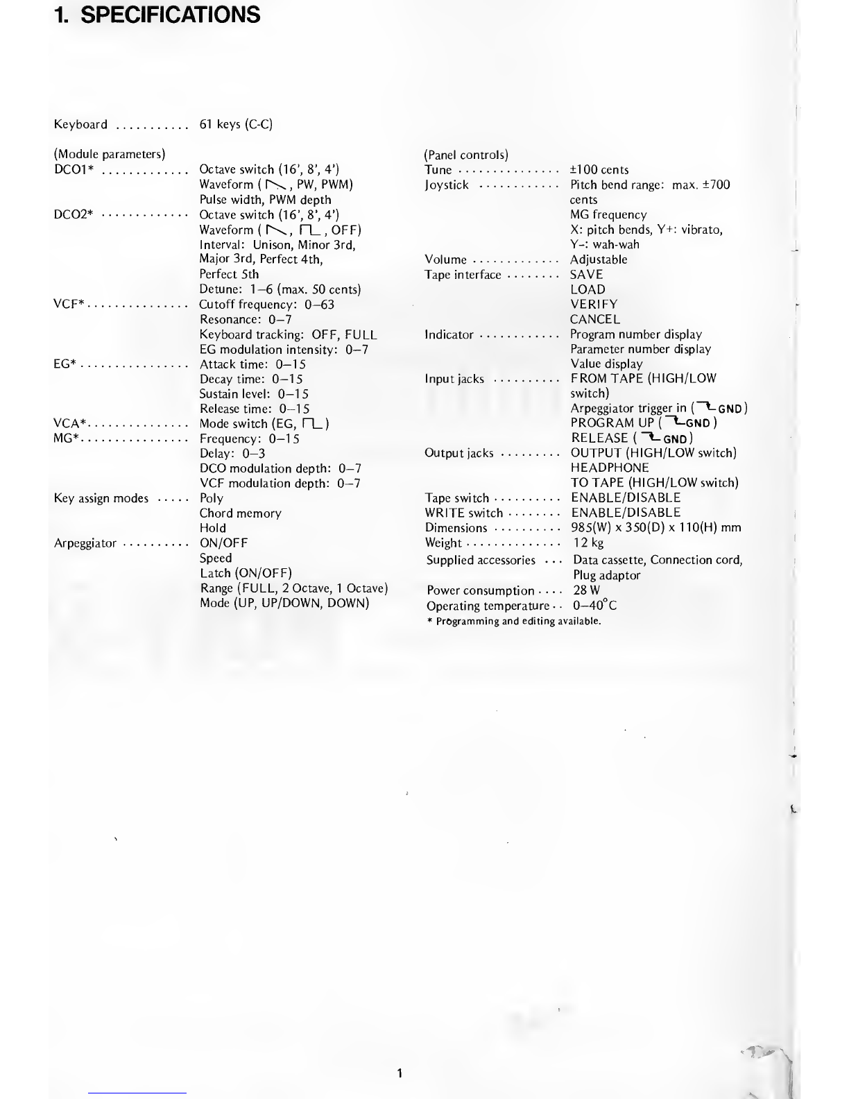
Korg POLY-61 User manual

PROGRAMMABLE
POLYPHONIC
SYNTHESIZER
SERVICE
MANUAL
POIY-61
CONTENTS
1.
SPECI
U
‘’CATIONS.
1
2.
STRUCTURAL
DIAGRAM.
2
3.
BLOCK
DIAGRAM.
4
4.
CIRCUIT
DIAGRAM.
5
5.
REFERENCE
DATA.
9
6.
PC
BOARD
.
10
7.
SETTING
CHAS
iS.
18
8.
CHECK
AND
ADJUSTMENT
PROCEDURE
....
19
9.
PARTS
LIST
.
25
v
\
KEIO
ELt-CTHONIC
LABORATORY
CORPORATION
TOKYO/JAPAN

1.
SPECIFICATIONS
Keyboard
.
.
61
keys
(C-C)
(Module
parameters)
(Panel
controls)
DCOI*
.
.
Octave
switch
(16’,
8’,
4’)
Tune.
±100
cents
Waveform
(r\
,
PW,
PWM)
Joystick
.
Pitch
bend
range:
max.
±700
Pulse
width,
PWM
depth
cents
DC02*
.
•
Octave
switch
(16’,
8’,
4’)
MG
frequency
Waveform
(D\,
n_,OFF)
X:
pitch
bends,
Y+:
vibrato,
Interval:
Unison,
Minor
3rd,
Y-:
wah-wah
Major
3rd,
Perfect
4th,
Volume.
Adjustable
Perfect
5th
Tape
interface.
SAVE
Detune:
1—6
(max.
50
cents)
FOAD
VCF*.
■
Cutoff
frequency:
0—63
VERIFY
Resonance:
0—7
CANCEF
Keyboard
tracking:
OFF,
FUFF
Indicator.
Program
number
display
EG
modulation
intensity:
0—7
Parameter
number
display
EG*.
■
Attack
time:
0—15
Value
display
Decay
time:
0—15
Input
jacks
.
FROM
TAPE
(HIGH/FOW
Sustain
level:
0—15
switch)
Release
time:
0—15
Arpeggiator
trigger
in
(~
*-GND
VCA*.
■
Mode
switch
(EG,
n_)
PROGRAM
UP
Ct-GND)
MG*.
•
Frequency:
0—15
REFEASE
(
“t-GND)
Delay:
0-3
Output
jacks.
OUTPUT
(HIGH/FOW
switch)
DCO
modulation
depth:
0—7
HEADPHONE
VCF
modulation
depth:
0—7
TO
TAPE
(HIGH/FOW
switch)
Key
assign
modes
•
•
•
■
•
Poly
Tape
switch.
ENABFE/DISABFE
Chord
memory
WRITE
switch.
ENABFE/DISABFE
Hold
Dimensions.
■
985(W)
x
350(D)
x
110(H)
mm
Arpeggiator.
•
ON/OFF
Weight.
12
kg
Speed
Supplied
accessories
•
•
•
Data
cassette,
Connection
cord,
Fateh
(ON/OFF)
Plug
adaptor
Range
(FUFF,
2
Octave,
1
Octave)
Power
consumption
•
■
•
•
28
W
Mode
(UP,
UP/DOWN,
DOWN)
Operating
temperature
•
■
0-40°
C
*
Programming
and
editing
available.
i

2.
STRUCTURAL
DIAGRAM
PART
NO.
PART
NAME
REMARKS
1
Panel
KOC-C20124
2
Metal
fittings
of
phone
jack
KOC-C30205
3
Led
cover
KOC-E40129
4
Tact
SW
knob
A
KOC-E30042
(Ivory)
5
Tact
SW
knob
B
No.
1
KOC-E30043
(Ivory)
6
Tact
SW
knob
B
No.
2
KOC-E30043
(Red)
7
Tact
SW
escutcheon
1
KOC-E20047
8
Tact
SW
escutcheon
2
KOC-E20048
9
Tact
SW
escutcheon
3
KOC-E
20049
10
Tact
SW
escutcheon
8
KOC-E20050
11
Rotary
VR
knob
KOC-E40087
12
Slide
SW
knob
(High
6m/m
black)
13
Slide
SW
mask
KOC-F40222

LEVER
KNOB
PART
NO.
PART
NAME
REMARK
1
Wooden
case
KOC-D10014
2
Keyboard
ESK-70
3
PC
board
rail
4
Control
panel
KOC-20040
5
Joystick
6
Radiation
board
KOC-C30207
7
Shielding
sheet
KOC-F40227
8
Bushing
TA-305
(Black)
9
••
TB-300
(Black)
10
-
TA-310
11
■■
TB-300
12
Felt
KOC-F40186
13
Shielding
sheet
14
Fuse
seal
Fuse
250V
1A
(T1
A)
15
"
Fuse
250V
2A
(T2A)
3

3.
BLOCK
DIAGRAM
4

4.
CIRCUIT
DIAGRAM
KLM-475
(OLD
PRODUCTION)
C4I
KIM-475
CPU
BOARD
ic
.
.
CN3U
4
5M
TOTAK
4
-
?
&fc
0
8
j
[rg
2903
ica»
|
HW40OJ
8049
n
Vnn
ir.XODO
^C33
7
D1
03
X)
X2
04
DC
D7
RD
WH
SS
E
A
PSEN
PIG
P11
PROG
P12
PH
P14
P15
PI
6
P17
P7G
P2.1
P22
Tt
P23
P24
TQ
P25
P2G
1
NT
P27
rrri
ba6
|03M
|
-.CH-25B
C6
ctT
m
A
sr
™
^
[tS
W
~3,
(33
XTAL
XI
4
«*(!»,
8M)i
8049
IC
1
D
QJ
*•0217
D1
*tc
0
2
D
3
D4
XI
D5
x2
D
6
HTSTr
D
7
$r
ALE
EA
Wo
psCn
Wfl
PROG
PIO
PM
P
1
2
P13
PH
Plb
Plft
P17
P20
P2I
P22
T
1
P2
3
P24
TO
P2
5
P2
G
»
NT
P27
5


KLM-476,
477,
478,
479,
481,
482
(OLD
PRODUCTION)
KLM-478
ANT
I
BOARD
CN-34b
7

KLM-508,
477,
479,
481,
482
(NEW
PRODUCTION)
KLM
—508
SYNTH
BOARD

amoK:
[xnxixi
iit'ir.ftrra
a
«a—
oHt-e
!
■
—aa
t-jj—
■
jajy&a
gj^yis
gUl
ggi

VO
I
CE6
|
Ce0
j
VOICE4
IC40I
1C
SOI
;tp6oz.
:
j
^
02
g
si
;
t
P402
oo
!TP302
m
o£
[TP202-,
o
2TPI02
J605
O.o
(£>
)
CD
oc\cc
CNi^B
£
3
CNt«;
R407
J407
—Wr—
R40
8
Ja
i
JC4Q3
IQ
60
3
1C
503
TP
601
IC602
(C502
1C
303
IC203
1C
103
VCA
ADJ
VR603
ADJ
■
sf
in
ADJ
—
VR2Q3
VR30I
§
"VR302
VR602
VR502
VR503
VR403
VR402
IC509
VR202
VRlOl
VRI02
VRI032
JS20
"""
1
ttr
n
R5
^
Rs
3vw—
□
o
fo
*10504
O
O
«fi
■
X5Q7
ft
to
»ft
m
3
\
St°oS
J220
=
J22I
=
00
05
o
C207
0405
10505
IC606
10405
tC
406
IC305
IC306
IC205
1C
206
C4II
Hh
C4I2-.
CN'ia'ti
J326
IC207
IC
6
0
8
1C
5
08
10408
tC308
c*JL
IC208
<m«4»
r\j
~I
TiT
VR604
VR504
VR404
/
VR304
VR204

Ss
HTTTnTJ
CN27A1
TUNE
J34

4
P


KLM-508
R
I
O
I
VOICE!
RI02
RI03T.P*02
ICIOI
|
M
w
R20I
!CIOI
I
I
IN
IV
J
IC20I
|
g
□
ite'i
□
ilMi
by
I
Ls
V
=^
oz
jjisj
Cl04
RI07L-W
L_1
—
VA
—
5
C204
R2
07
l-l
u
n<o
Lkiij
VOICE2
R202_
R203,
T
'
P202
V0ICE3
R302
R303^S-
302
V0ICE4
R402
R
403
if-
40
2
J
1
14
ICI03
""
yi
x>;.
lilO
•
T
1
I-DU
I
-
Plllliili
5
n
§
g~c!
/s
^
f
i
*
iCf
J609
I
J
610
IC602
=
D601
R61
*F60|
J
R6I2
J
5
14
i.c£o§
-
J2I3
WW'*,"
~~
,,
|
®
&
A
,
_
c;-
IC4Q5
IC505
*)
1
IC605
£-a-
1C305
^
i
_
i
J
6
13
UJSwffiiyJ
fTLIlfWK
i
m
MINI
iftat
O-tttteit
□
-
4
W8aP
U
=
i
ltft8y|P
□
i
H
I
m-
16

KLM-509
CN28A
CN300
-
-XI
C3
-
W
U©*
r3
*,-aw-
©
H
.06-
-
,oue
R52
CRISTA
5
@
-Wv-
©
R57
/
©
O
-2\W-
RS8
R59
»
®-VW-®
RS4
®
tt-Wr-
T
R60
*
«-W\-@R€l
@-W\-®R62
i-w*-o
«£avv-«
#-vw-@R63
CN33A
K>,M-6a3fi
ff'Sa'
“
,**
*
£
R7I
-W-0-#
R
7
2^-W^0
\
tl-VW^#R30
“O
'
#
■
—\Av-
^
5
R76
,
■
HMm
aferii
i
i
■
1#|
•
<3
s
...
^
■
iAAAr-
IM
T
R84
j
,,
©~©-Wr-
#
i
«
o
/
■
“
O
©-VVV-0
,;®
T
r
«''
ag
,
y^—Sr-
|
'
R94^-VW0
2
©
»
~'g<o<
:
s
*
8
*
#
i
S
#
«
«
«
e'»
«
4
# #
«
s
e
R95
-3-WV-ft,.oi
1
®
CPU
%
i
R96
—\W
:
C)
,
<r
.
0:
«
°
BOARD
KLM-
S
OSA
R9'
w-
$
«mk>
?
•*
it
<£
r-
to
§.,£
g
..
.
'
p.-,
S
n
S
«„
iEEEiiSif
-
G*
"
•
■
•
u
si
la
o
:
I
1
i
a
-a
Ai.
ss%
m,
^
-s
..
$3
If
.
**
,
C40
R150
v
-WV-
0
f
*.
RI4S
1
i'-V/r
A-
T-*AV-
?I
P*
^vC53
R222
T
©
S
©-VVV-,©*©
17

5.
REFERENCE
DATA
IC8255A-5
PROGRAMMABLE
PERIPHERAL
INTERFACE
PIN
CONFIGURATION
8255A
BLOCK
DIAGRAM
PIN
NAMES
d
7
-
d
0
DATA
BUS
(Bl
DIRECTIONAL)
RESET
RESET
INPUT
CS
CHIP
SELECT
RD
READ
INPUT
WR
RITE
INPUT
AO,
A1
PORT
ADDRESS
PA7-PA0
PORT
A
(BIT)
PB7-PB0
PORT
B
(BIT)
PC7-PC0
PORT
C
(BIT)
Vcc
+5
VOLTS
GND
0
VOLTS
BI-DIRECTIONAL
DATA
BUS
IC8253C-5
PROGRAMMABLE
INTERVAL
TIMER
BLOCK
DIAGRAM
PIN
NAMES
DATA
BUS
(8
BIT)
_
COUNTER
CLOCK
INPUTS
COUNTER
GATE
INPUTS
COUNTER
OUTPUTS
_
READ
COUNTER
_
WRITE
COMMAND
OR
DATA
CHIP
SELECT
_
COUNTER
SELECT
_
4-5
VOLTS
_
GROUND
PIN
CONFIGURATION
OUT
o
□
10
24
JVcc
23
3wR
22
^RD
21
DCS
20
3
A
,
8253
19
3
A
o
18
3
CLK
2
17
3
OUT
2
16
3
GATE
2
15
3
CLK
1
14
3
GATE
1
13
3
OUT
1
IC8049
SINGLE
COMPONENT
8-BIT
MICROCOMPUTER

PIN
DESCRIPTION
Designation
Pin
#
Function
Designation
Pin
#
Vss
20
Circuit
GND
potential
RD
8
Q
Q
>
26
+5V
during
operation.
Low
power
standby
pin.
V
C
c
40
Main
power
supply:
+5V
during
operation.
PROG
25
Output
strobe
for
8243
I/O
expander.
RESET
4
P10-P17
Port
1
27-34
8-bit
quasi-bidirectional
port.
P20-P27
21-24
8-bit
quasi-bidirectional
port.
WR
10
Port
2
35-38
P20-P23
contain
the
four
high
order
program
counter
bits
during
an
external
program
memory
fetch
and
serve
as
a
4-bit
I/O
expander
bus
for
8243
ALE
11
D0-D7
12-19
True
bidirectional
port
which
can
BUS
be
written
or
read
synchronously
using
the
RD,
WR
strobes.
The
Port
can
also
be
statically
latched.
Contains
the
8
low
order
program
counter
bits
during
an
external
PSEN
9
program
memory
fetch,
and
receives
the
addressed
instruction
under
the
control
of
PSEN.
Also
contains
the
address
and
data
during
an
external
RAM
data
store
instruction,
under
control
of
ALE,
RD,
and
WR.
SS
5
TO
1
Input
pin
testable
using
the
con¬
ditional
transfer
instructions
JTO
and
JNTO.
TO
can
be
designated
as
a
clock
output
using
ENTO
CLK
instruction.
EA
7
T1
39
Input
pin
testable
using
the
JT1,
and
JNT1
instructions.
Can
be
des¬
ignated
the
timer/counter
input
using
the
STRT
CNT
instruction.
XTAL1
2
INT
6
Interrupt
input.
Initiates
an
inter¬
rupt
if
interrupt
is
enabled.
Inter-
XTAL2
3
rupt
is
disabled
after
a
reset.
Also
testable
with
conditional
jump
instruction.
(Active
low)
Function
Output
strobe
activated
during
a
BUS
read.
Can
be
used
to
enable
data
onto
the
BUS
from
an
external
device.
Used
as
a
Read
Strobe
to
External
Data
Memory.
(Active
low)
Input
which
is
used
to
initialize
the
processor.
Also
used
during
verifi¬
cation,
and
power
down.
(Active
low)
(Non
TTL
V||-|)
Output
strobe
during
a
BUS
write.
(Active
low)
Used
as
write
strobe
to
External
Data
Memory.
Address
Latch
Enable.
This
signal
occurs
once
during
each
cycle
and
is
useful
as
a
clock
output.
The
negative
edge
of
ALE
strobes
address
into
external
data
and
pro¬
gram
memory.
Program
Store
Enable.
This
output
occurs
only
during
a
fetch
to
exter¬
nal
program
memory.
(Active
low)
Single
step
input
can
be
used
in
con¬
junction
with
ALE
to
"single
step"
the
processor
through
each
in¬
struction.
(Active
low)
External
Access
input
which
forces
all
program
memory
fetches
to
re¬
ference
external
memory.
Useful
for
emulation
and
debug,
and
essential
for
testing
and
program
verification.
(Active
high)
One
side
of
crystal
input
for
inter¬
nal
oscillator.
Also
input
for
exter¬
nal
source.
(Not
TTL
Compatible)
Other
side
of
crystal
input.
1C
M58981P-45
4096-BIT
(1024-WORD
BY
4-BIT)
CMOS
STATIC
RAM
PIN
CONFIGURATION
BLOCK
DIAGRAM
ADDRESS
INPUTS
V
cc
(5V)
GND
(OV)
DATA
INPUT/
OUTPUT

8.
CHECK
AND
ADJUSTMENT
PROCEDURE
Caution:
Everything
has
been
completely
adjusted
at
the
factory
prior
to
shipment.
Therefore,
never
turn
any
VRs
other
than
those
required
for
servicing.
*
After
turning
on
power,
wait
at
least
ten
minutes
before
beginning
tests
and
adjustments.
*
Circuit
board
numbers
change
from
711801
,
as
divided
into
new
production
and
old
production
lots.
Old
circuit
board
numbers
are
in
parentheses.
*
If
replacing
KLM-508
(KLM-476)
ICs
101~601
NJM072DH,
be
sure
to
use
new
ones
of
the
same
color
selection.
Others
will
cause
irregularities
in
sawtooth
wave
amplitude
and
PW/PWM
duty.
*
Adjustment
setting
charts
are
on
a
separate
page.
Please
refer
to
it
for
correct
settings.
*
Data
cassette
(Data
of
adjustment
procedure)
showing
the
setting
is
available
for
repairing
and
adjusting.
Please
load
the
cassette
on
and
select
a
program
you
need
each
time.
1.
KLM-480
(Power
supply
check
and
adjustment).
Use
DVM
(digital
voltmeter)
to
test
each
check
point
on
KLM-480.
Confirm
that
voltages
are
within
specifications
listed
below.
(1)
+15V:
+14.95V~+15.05V;
Adjust
VR1
if
necessary.
(2)
-15V:
-14.70V~-15.30V
(3)
+5V:
+4.75V-+5.25V
2.
KLM-477
(CLOCK
BOARD
check
and
adjustment).
1.
TOTAL
TUNE.
1)
Set
to
PROGRAM
11.
2)
Hold
A3
(440Hz)
and
set
TUNE
knob
to
center.
3)
Connect
output
to
tuner
and
adjust
VR5
to
obtain
reading
within
±5
cent.
4)
Confirm
+100
cent
(±20
cent)
when
TUNE
knob
is
turned
all
the
way
clockwise
(#).
5)
Confirm
—90
cent
(±20
cent)
when
the
TUNE
knob
is
turned
all
the
way
counterclockwise
(b).
2.
JOYSTICK.
1)
Set
to
PROG
RAM
11.
2)
Hold
A3
and
adjust
TUNE
knob
to
obtain
0
cent
reading
on
tuner.
3)
Set
BEND
knob
to
10
and
confirm
+700
cent
(0~+15
cent)
(E
above
A3)
when
joystick
is
at
maximum
pitch
bend
up
position.
Adjust
VR6
if
necessary.
4)
Confirm
-700
cent
(-15~0
cent)
(D)
when
joystick
is
at
maximum
pitch
bend
down
position.
Adjust
VR7
if
necessary.
5)
Adjust
TUNE
knob
to
obtain
0
cent
reading.
Then
use
joy
stick
to
apply
vibrato
and
pitch
bends
(up
and
down),
slowly
returning
the
joystick
to
the
center
position.
Confirm
that
pitch
is
still
within
±2
cent.
6)
Connect
oscilloscope
to
CN39—1,
apply
vibrato
and
set
FREQUENCY
knob
to
5.
Confirm
vibrato
at
'
rate
of
about
5~6Hz.
7)
In
same
way,
confirm
about
10Hz
when
FRE¬
QUENCY
knob
is
at
10,
and
about
0.12Hz
when
knob
is
at
0.
8)
Set
FREQUENCY
to
0
and
apply
vibrato
at
maxi¬
mum
intensity.
Confirm
tuner
readout
variation
from
+60~+120
cent
to
—
60~—120
cent.
There
should
be
no
more
than
30
cent
difference
between
the
amount
of
swing
to
the
left
and
right.
3.
K
L
M
-
508
(KLM-478)
(ANTI
BOARD).
1.
ANTI-LOG.
1)
Set
to
PROGRAM
12
and
put
same
note
into
CHORD
MEMORY
six
times.
In
other
words,
turn
on
HOLD
and
play
same
note
six
times,
then
turn
on
CHORD
MEMORY.
Confirm
that
NJM-072
(IC101
—601)
are
all
the
same
color.
2)
Check
KLM-508
(KLM-476)
(SYNTHE-BOARD)
TP1
with
DVM
and
confirm
9.80V~10.20V.
3)
Connect
oscilloscope
GND
to
TPl
and
check
TP102~
TP602.
Note:
TPl
is
not
at
ground
(0V).
4)
Play
Cl
and
confirm
Fig-1
waveform
for
all
six
voices.
5)
N
ext,
expand
oscilloscope
range
and
check
six
voices,
finding
the
one
with
the
greatest
amplitude
Fig-2
.
Confirm
that
difference
between
largest
and
smallest
amplitude
is
within
1.0V.
After
finding
voices
with
largest
amplitude,
perform
check
and
adjustment
procedures
A
through
I,
below,
for
that
voice.
(Adjust
oscilloscope
GND
before¬
hand.)
Other manuals for POLY-61
3
Table of contents
Other Korg Synthesizer manuals

Korg
Korg Z3 User manual

Korg
Korg X5D User manual

Korg
Korg MS-20 Kit User manual

Korg
Korg Wavedrum User manual

Korg
Korg RK-100S User manual

Korg
Korg PS60 Instructions for use

Korg
Korg KROSS 2 Series User manual

Korg
Korg Polyphonic Ensemble User manual

Korg
Korg X5DR AI2 SYNTHESIS MODULE User manual

Korg
Korg PS-3300 User manual