Lattice Semiconductor Smart Socket User manual

Smart Socket
User Guide
FPGA-UG-02046 Version 1.1
April 2018

Smart Socket
User Guide
© 2016-2018 Lattice Semiconductor Corp. All Lattice trademarks, registered trademarks, patents, and disclaimers are as listed at www.latticesemi.com/legal.
All other brand or product names are trademarks or registered trademarks of their respective holders. The specifications and information herein are subject to change without notice.
2 FPGA-UG-02046-1.1
Contents
1. Introduction ..................................................................................................................................................................4
2. Features ........................................................................................................................................................................4
3. Block Diagram ...............................................................................................................................................................5
4. Board Specifications .....................................................................................................................................................6
5. Software Requirements ................................................................................................................................................7
5.1. Generic Programming .........................................................................................................................................7
5.2. Specific Software Requirements for Certain Device Families ...........................................................................11
5.2.1. MachXO3 Device Family Programming.........................................................................................................11
5.2.2. ECP5 Device Family Programming ................................................................................................................11
5.2.3. L-ASC10 Device Programming.......................................................................................................................11
5.2.4. iCE40 Device Family Programming ...............................................................................................................16
5.2.5. CrossLink Device Family Programming .........................................................................................................19
6. Ordering Information..................................................................................................................................................21
Technical Support ...............................................................................................................................................................22
Appendix A. Smart Socket Board Schematics .....................................................................................................................23
Appendix B. Debugging.......................................................................................................................................................27
Revision History ..................................................................................................................................................................29

Smart Socket
User Guide
© 2016-2018 Lattice Semiconductor Corp. All Lattice trademarks, registered trademarks, patents, and disclaimers are as listed at www.latticesemi.com/legal.
All other brand or product names are trademarks or registered trademarks of their respective holders. The specifications and information herein are subject to change without notice.
FPGA-UG-02046-1.1 3
Figures
Figure 3.1. Smart Socket Programming Board Block Diagram..............................................................................................5
Figure 5.1. Getting Started ...................................................................................................................................................7
Figure 5.2. Scanning..............................................................................................................................................................7
Figure 5.3. Unable to Identify Device ...................................................................................................................................8
Figure 5.4. Identifying Correct Device ..................................................................................................................................8
Figure 5.5. Access Device Properties through Edit ...............................................................................................................8
Figure 5.6. Programming Options.........................................................................................................................................9
Figure 5.7. Bit File Selection .................................................................................................................................................9
Figure 5.8. Program Icon ......................................................................................................................................................9
Figure 5.9. Design Menu.......................................................................................................................................................9
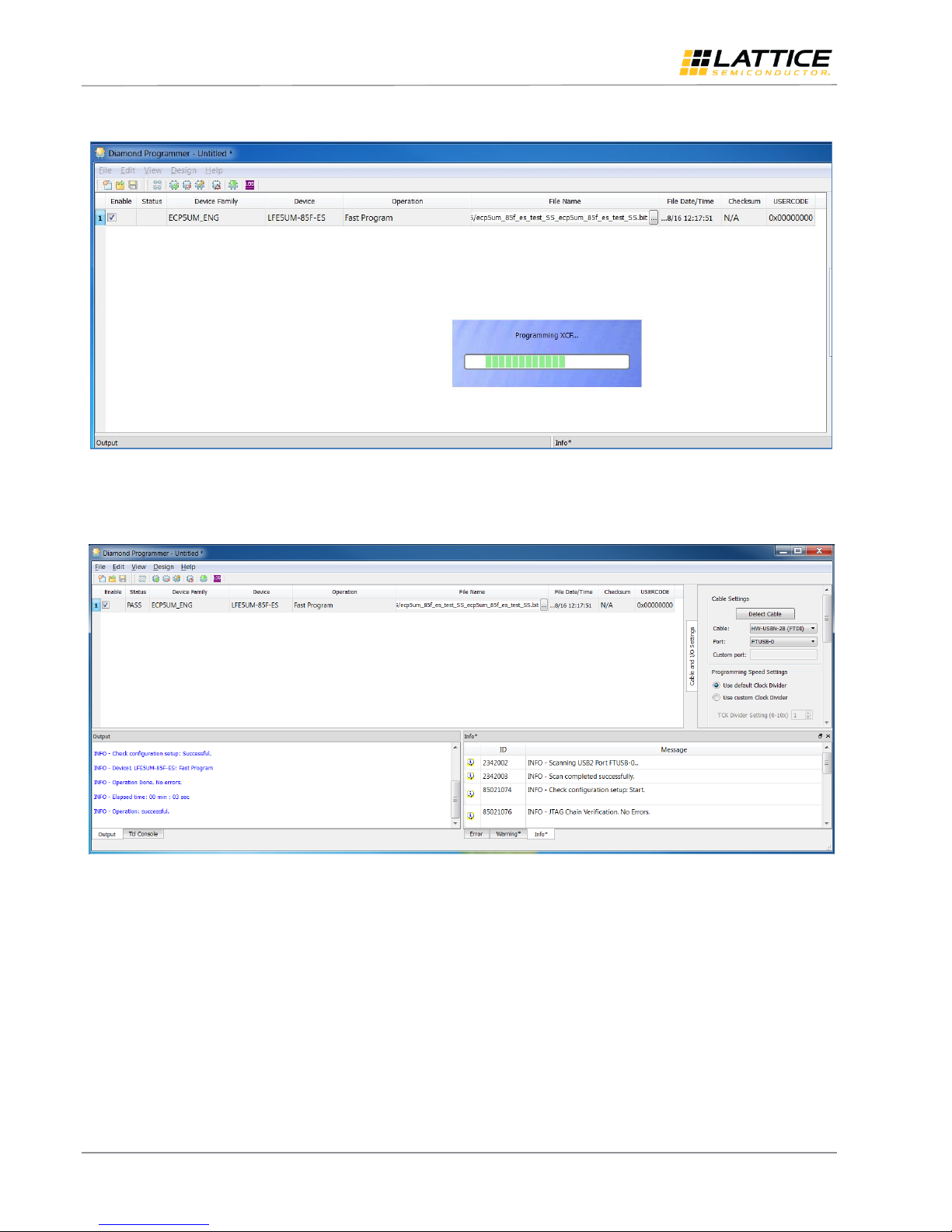
Figure 5.10. Programming in Progress................................................................................................................................10
Figure 5.11. Successful Programming.................................................................................................................................10
Figure 5.12. ASC Socket –Scanned MachXO2 Device ........................................................................................................11
Figure 5.13. ASC Socket –Operation ..................................................................................................................................11
Figure 5.14. ASC Socket –Device Properties ......................................................................................................................12
Figure 5.15. ASC Socket –Add External ASC Device ...........................................................................................................12
Figure 5.16. ASC Socket –ASC File Load Menu...................................................................................................................13
Figure 5.17. ASC Socket –Operation Menu........................................................................................................................14
Figure 5.18. Warning ..........................................................................................................................................................14
Figure 5.19. ASC Socket –Warning for MachXO2 ..............................................................................................................15
Figure 5.20. ASC Socket –Ready to Program Step .............................................................................................................15
Figure 5.21. ASC Socket –Programming.............................................................................................................................15
Figure 5.22. ASC Socket –Programming Completed ..........................................................................................................16
Figure 5.23. iCE40 Family –Scanning Failed .......................................................................................................................16
Figure 5.24. iCE40 Family –Device Family List ...................................................................................................................17
Figure 5.25. iCE40 Family –Select the Programming File...................................................................................................17
Figure 5.26. iCE40 Family –Program Icon ..........................................................................................................................17
Figure 5.27. iCE40 Family –Programming Completed Successfully ...................................................................................18
Figure 5.28. CrossLink Family –Scanning Failed.................................................................................................................19
Figure 5.29. CrossLink Family –Device Family List .............................................................................................................20
Figure 5.30. CrossLink Family –Select the Programming File ............................................................................................20
Figure 5.31. CrossLink Family –Program Icon ....................................................................................................................21
Figure 5.32. CrossLink Family –Programming Completed Successfully .............................................................................21
Figure A.1. USB Programming Interface .............................................................................................................................23
Figure A.2. Voltage Regulator and LEDs .............................................................................................................................24
Figure A.3. JTAG Bank and Connections .............................................................................................................................25
Figure A.4. VCC Core, Bypass Caps, and Test Points...........................................................................................................26
Figure B.1. Failed to Scan Device ........................................................................................................................................27
Figure B.2. Detect Cable (FTDI)...........................................................................................................................................27
Figure B.3. Scanning Completed.........................................................................................................................................28

Smart Socket
User Guide
© 2016-2018 Lattice Semiconductor Corp. All Lattice trademarks, registered trademarks, patents, and disclaimers are as listed at www.latticesemi.com/legal.
All other brand or product names are trademarks or registered trademarks of their respective holders. The specifications and information herein are subject to change without notice.
4 FPGA-UG-02046-1.1
1. Introduction
This document describes Smart Socket, the next generation programming solution, from Lattice Semiconductor. Smart
Socket replaces the legacy Lattice Model 300 and its associated Socket Adapters. Smart Socket uses the same JTAG-
based Lattice Diamond®Programmer programming software that is used with Lattice Semiconductor’s popular
evaluation and customer boards. Standard ESD environment and procedures should be followed when working with
loose devices and the Smart Socket.
2. Features
Each Smart Socket board is unique for a device family and package. Smart Socket boards have common features such
as:
Powered over simple USB cable
Power switch to remove power from the socket
Integrated FTDI USB interface to work directly with Lattice Programming tools
Power indicator LEDs
Convenient test points

Smart Socket
User Guide
© 2016-2018 Lattice Semiconductor Corp. All Lattice trademarks, registered trademarks, patents, and disclaimers are as listed at www.latticesemi.com/legal.
All other brand or product names are trademarks or registered trademarks of their respective holders. The specifications and information herein are subject to change without notice.
FPGA-UG-02046-1.1 5
3. Block Diagram
Figure 3.1 shows the high level blocks of a Smart Socket board. The four major blocks on the board are:
USB connector
USB-to-SPI/JTAG communication bridge
Board power regulator
Some product families, such as MachX02, have parts with different core supply voltage requirements. The
Smart Socket board jumper (J2) allows you to select between 1.2 V and 3.3 V core supply voltage. The selected
core supply voltage is indicated by LEDs located next to the jumper on the board.
Lattice Semiconductor Socket (family specific)
A switch controls power to the socket. Three separate LEDs indicate USB power, Socket Power and Programming Done
(Programming Done support varies by device family).
USB Connector
Lattice Semiconductor
FPGA Socket
Regulator
Green LED
ON/OFF Switch
Power from USB 5 V
Hardware Board
PC FTDI Chip
USB Power
USB to SPI/JTAG
Socket Power
USB Cable
Diamond
Programmer
Done*
Red LED
Blue LED
*Note: Programming Done support depends on the device family.
Figure 3.1. Smart Socket Programming Board Block Diagram

Smart Socket
User Guide
© 2016-2018 Lattice Semiconductor Corp. All Lattice trademarks, registered trademarks, patents, and disclaimers are as listed at www.latticesemi.com/legal.
All other brand or product names are trademarks or registered trademarks of their respective holders. The specifications and information herein are subject to change without notice.
6 FPGA-UG-02046-1.1
4. Board Specifications
The outline dimension is the same for all Smart Socket boards. The dimensions of the socket vary based on target
device family and package.
Board dimensions:
Width: 4 inch
Length: 6 inch
Height: < 2 inch
Electrical Specification:
+5 V @ 500 mA or less (provided by USB cable)
The complete list of sockets is available at: http://www.latticesemi.com/sockets

Smart Socket
User Guide
© 2016-2018 Lattice Semiconductor Corp. All Lattice trademarks, registered trademarks, patents, and disclaimers are as listed at www.latticesemi.com/legal.
All other brand or product names are trademarks or registered trademarks of their respective holders. The specifications and information herein are subject to change without notice.
FPGA-UG-02046-1.1 7
5. Software Requirements
Smart Socket is supported by Lattice Diamond®Programmer. The latest version of the Lattice Diamond Programmer
can be downloaded at:
http://www.latticesemi.com/en/Products/DesignSoftwareAndIP/FPGAandLDS/LatticeDiamond.aspx
Smart Socket works with the Lattice Diamond Programmer using only a USB cable. Connect the cable from the Smart
Socket to a PC, and use the cable search feature in Lattice Diamond Programmer to establish the programming link. The
steps to program a device are described below.
5.1. Generic Programming
To program the device:
1. Launch the Lattice Diamond Programmer software. The Diamond Programmer Getting Started dialog box appears
as shown in Figure 5.1.
Figure 5.1. Getting Started
2. Click OK. The Diamond Programmer automatically starts scanning. The scanning page appears as shown in
Figure 5.2.
Figure 5.2. Scanning

Smart Socket
User Guide
© 2016-2018 Lattice Semiconductor Corp. All Lattice trademarks, registered trademarks, patents, and disclaimers are as listed at www.latticesemi.com/legal.
All other brand or product names are trademarks or registered trademarks of their respective holders. The specifications and information herein are subject to change without notice.
8 FPGA-UG-02046-1.1
When the device scanning is completed, the Diamond Programmer tool shows the device present in socket in the
Device tab. If the Diamond Programmer is unable to identify the device in socket, the device family name is
highlighted with a yellow background under Device as shown in Figure 5.3. Some device families may not support
the scan operation. For details, see the Software Requirements for Specific Device Families section.
Figure 5.3. Unable to Identify Device
In such case, click in the yellow highlighted area and select the appropriate device by matching the device name on
the package with the dropdown list in the Device tab. Select the correct device on the dropdown list, and the
yellow background highlighting disappears as shown in Figure 5.4.
Figure 5.4. Identifying Correct Device
3. Verify that the desired Operation is specified, and update if necessary. To update the operation, select the device
row so that it is highlighted in blue as shown in Figure 5.5. On the menu bar, click Edit, and on the dropdown menu
click Device Properties as shown in Figure 5.5.
Figure 5.5. Access Device Properties through Edit

Smart Socket
User Guide
© 2016-2018 Lattice Semiconductor Corp. All Lattice trademarks, registered trademarks, patents, and disclaimers are as listed at www.latticesemi.com/legal.
All other brand or product names are trademarks or registered trademarks of their respective holders. The specifications and information herein are subject to change without notice.
FPGA-UG-02046-1.1 9
4. Select the appropriate programming file by clicking the Browse button in the Programming Options section as
shown in Figure 5.6.
5. Click OK.
Figure 5.6. Programming Options
6. The selected file is shown under File Name in the Diamond Programmer main interface as shown in Figure 5.7.
Figure 5.7. Bit File Selection
7. To start programming the device, click the Program icon shown in Figure 5.8.
Figure 5.8. Program Icon
You can also click Design and select Program as shown in Figure 5.9.
Figure 5.9. Design Menu

Smart Socket
User Guide
© 2016-2018 Lattice Semiconductor Corp. All Lattice trademarks, registered trademarks, patents, and disclaimers are as listed at www.latticesemi.com/legal.
All other brand or product names are trademarks or registered trademarks of their respective holders. The specifications and information herein are subject to change without notice.
10 FPGA-UG-02046-1.1
Figure 5.10 shows that the programming of device is in progress.
Figure 5.10. Programming in Progress
8. When the programming of the device is completed, the Status option changes to PASS and Operation: successful
message appears in the Output console as shown in Figure 5.11.
Figure 5.11. Successful Programming
On the board, the green Done LED is lit when the device is successfully programmed (Done LED behavior is device
dependent, see the Software Requirements for Specific Device Families section for details).

Smart Socket
User Guide
© 2016-2018 Lattice Semiconductor Corp. All Lattice trademarks, registered trademarks, patents, and disclaimers are as listed at www.latticesemi.com/legal.
All other brand or product names are trademarks or registered trademarks of their respective holders. The specifications and information herein are subject to change without notice.
FPGA-UG-02046-1.1 11
5.2. Software Requirements for Specific Device Families
5.2.1. MachXO3 Device Family Programming
The programming of MachXO3 device family follows steps similar to the process described in the Generic Programming
section. Done is not a dedicated output in the MachXO3 device family. Done LED indication is not supported.
5.2.2. ECP5 Device Family Programming
The programming of ECP5 device family follows steps similar to the process described in the Generic Programming
section. When the programming of these devices is completed successfully, the Done LED is lit.
5.2.3. L-ASC10 Device Programming
To program the ASC device:
1. Launch the Lattice Diamond Programmer software.
The Diamond Programmer automatically starts scanning the device and detects the MachXO2 device as shown in
Figure 5.12.
Figure 5.12. ASC Socket –Scanned MachXO2 Device
2. Double click in the box under Operation as shown in Figure 5.13.
Figure 5.13. ASC Socket –Operation
3. The Device Properties dialog box appears as shown in Figure 5.14. In the Access Mode dropdown list, select PTM
Programming. Note that in the main interface, PTM Bypass is indicated under Operation.

Smart Socket
User Guide
© 2016-2018 Lattice Semiconductor Corp. All Lattice trademarks, registered trademarks, patents, and disclaimers are as listed at www.latticesemi.com/legal.
All other brand or product names are trademarks or registered trademarks of their respective holders. The specifications and information herein are subject to change without notice.
12 FPGA-UG-02046-1.1
Figure 5.14. ASC Socket –Device Properties
4. Add an external ASC device, by clicking the button as shown in Figure 5.15. The Device Properties dialog box
appears as shown in Figure 5.16.
Figure 5.15. ASC Socket –Add External ASC Device

Smart Socket
User Guide
© 2016-2018 Lattice Semiconductor Corp. All Lattice trademarks, registered trademarks, patents, and disclaimers are as listed at www.latticesemi.com/legal.
All other brand or product names are trademarks or registered trademarks of their respective holders. The specifications and information herein are subject to change without notice.
FPGA-UG-02046-1.1 13
Figure 5.16. ASC Socket –ASC File Load Menu
5. Select the programming file by clicking the Browse button . In the Device Properties dialog box, select the
*ASCx.hex file.
6. From the Operation dropdown list, select ASC Erase, Program, Verify.

Smart Socket
User Guide
© 2016-2018 Lattice Semiconductor Corp. All Lattice trademarks, registered trademarks, patents, and disclaimers are as listed at www.latticesemi.com/legal.
All other brand or product names are trademarks or registered trademarks of their respective holders. The specifications and information herein are subject to change without notice.
14 FPGA-UG-02046-1.1
Figure 5.17. ASC Socket –Operation Menu
The warning shown in Figure 5.18 may appear if the selected external ASC device and the File targeting device do
not match.
Figure 5.18. Warning
7. Click OK. The same warning appears in the output console window as shown Figure 5.19.

Smart Socket
User Guide
© 2016-2018 Lattice Semiconductor Corp. All Lattice trademarks, registered trademarks, patents, and disclaimers are as listed at www.latticesemi.com/legal.
All other brand or product names are trademarks or registered trademarks of their respective holders. The specifications and information herein are subject to change without notice.
FPGA-UG-02046-1.1 15
Figure 5.19. ASC Socket –Warning for MachXO2
Under Operation, PTM Bypass is indicated. The File Name field is greyed out (to prevent adding a new file) as shown in
Figure 5.20.
Figure 5.20. ASC Socket –Ready to Program Step
8. Program the ASC device through the MachXO2 device on the Smart Socket board by clicking the Program icon
as shown in Figure 5.21.
Figure 5.21. ASC Socket –Programming
9. When the programming of the device is completed, the Status option changes to PASS and Operation: successful
message appears in the Output console as shown in Figure 5.22. During the programming activity the MXO2_SDA
and MXO2_SCL LED light blink on the board showing communication between the MachXO2 and ASC devices. Done
is not a dedicated output in the MachXO2 family. Done LED indication is not supported.

Smart Socket
User Guide
© 2016-2018 Lattice Semiconductor Corp. All Lattice trademarks, registered trademarks, patents, and disclaimers are as listed at www.latticesemi.com/legal.
All other brand or product names are trademarks or registered trademarks of their respective holders. The specifications and information herein are subject to change without notice.
16 FPGA-UG-02046-1.1
Figure 5.22. ASC Socket –Programming Completed
5.2.4. iCE40 Device Family Programming
To program the iCE40 device:
1. Launch the Lattice Diamond Programmer software.
The scanning of the device fails because the Scan operation is supported over JTAG interface only, and the iCE40
family of devices uses SPI interface for programming. See Figure 5.23.
Figure 5.23. iCE40 Family –Scanning Failed
2. Manually select the device by choosing the following options as shown in Figure 5.24.
Device Family: iCE5LP (select the appropriate device from the dropdown list)
Device: iCE5LP1K (choose the size of the device based on the device present in the socket)

Smart Socket
User Guide
© 2016-2018 Lattice Semiconductor Corp. All Lattice trademarks, registered trademarks, patents, and disclaimers are as listed at www.latticesemi.com/legal.
All other brand or product names are trademarks or registered trademarks of their respective holders. The specifications and information herein are subject to change without notice.
FPGA-UG-02046-1.1 17
Figure 5.24. iCE40 Family –Device Family List
3. Select the programming file to program the iCE40 device by double clicking the Browse button under File Name
as shown in Figure 5.25.
Figure 5.25. iCE40 Family –Select the Programming File
4. Click the Program icon to program the device as shown in Figure 5.26.
Figure 5.26. iCE40 Family –Program Icon
5. When the programming of the device is completed, the Status option changes to PASS and Operation: successful
message appears in the Output console as shown in Figure 5.27.

Smart Socket
User Guide
© 2016-2018 Lattice Semiconductor Corp. All Lattice trademarks, registered trademarks, patents, and disclaimers are as listed at www.latticesemi.com/legal.
All other brand or product names are trademarks or registered trademarks of their respective holders. The specifications and information herein are subject to change without notice.
18 FPGA-UG-02046-1.1
Figure 5.27. iCE40 Family –Programming Completed Successfully

Smart Socket
User Guide
© 2016-2018 Lattice Semiconductor Corp. All Lattice trademarks, registered trademarks, patents, and disclaimers are as listed at www.latticesemi.com/legal.
All other brand or product names are trademarks or registered trademarks of their respective holders. The specifications and information herein are subject to change without notice.
FPGA-UG-02046-1.1 19
5.2.5. CrossLink Device Family Programming
To program the CrossLink Device:
1. Launch the Lattice Diamond Programmer software.
The scanning of the device fails as the Scan operation is supported over JTAG interface only, and the CrossLink
family of devices uses SPI interface for programming. See Figure 5.28.
Figure 5.28. CrossLink Family –Scanning Failed
2. Manually select the device by choosing the following options as shown in Figure 5.29.
Device Family: LIFMD (select the appropriate device from the dropdown list)
Device: LIF-MD6000 or LIA-MD6000 (choose between industrial or automotive grade of CrossLink based on the
device present in the socket)

Smart Socket
User Guide
© 2016-2018 Lattice Semiconductor Corp. All Lattice trademarks, registered trademarks, patents, and disclaimers are as listed at www.latticesemi.com/legal.
All other brand or product names are trademarks or registered trademarks of their respective holders. The specifications and information herein are subject to change without notice.
20 FPGA-UG-02046-1.1
Figure 5.29. CrossLink Family –Device Family List
3. Select the programming file that you want to program in the CrossLink device by double clicking the Browse button
under File Name as shown in Figure 5.30.
Figure 5.30. CrossLink Family –Select the Programming File
4. Click the Program icon to program the device as shown in Figure 5.31.
Table of contents
Other Lattice Semiconductor Accessories manuals