Maxtang BYT60 User manual

BYT-60 Mini ITX Motherboard

Copyright
© 2022 Shenzhen Maxtang Computer Co., Ltd. All rights reserved. No part of this publication may be reproduced,
copied, stored in a retrieval system, translated into any language, or transmitted in any form or by any means,
electronic, mechanical, photocopying, or otherwise, without the prior written consent of Shenzhen Maxtang
Computer Co., Ltd (hereinafter referred to as “Maxtang”).
Disclaimer
Maxtang reserves the right to make changes and improvements to the products described in this document without
prior notice. Every effort has been made to ensure the information in the document is correct; however, Maxtang
does not guarantee this document is error-free.
Maxtang assumes no liability for incidental or consequential damages arising from misapplication or inability to use
the product or the information contained herein, nor for any infringements of rights of third parties, which may result
from its use.
Trademarks
All the trademarks, registrations, and brands mentioned herein are used for identification purposes only and may be
trademarks and/or registered trademarks of their respective owners.

Shenzhen Maxtang Computer Co., Ltd
1
BYT-60 Mini ITX Motherboard
User Manual
(Version 5.1)

Shenzhen Maxtang Computer Co., Ltd
2
Contents
BYT-60 Mini ITX Motherboard........................................................................................................ 1
Chapter 1 Product Introduction...................................................................................................... 3
1.1 Parameters................................................................................................................................ 3
Chapter 2 Hardware........................................................................................................................ 4
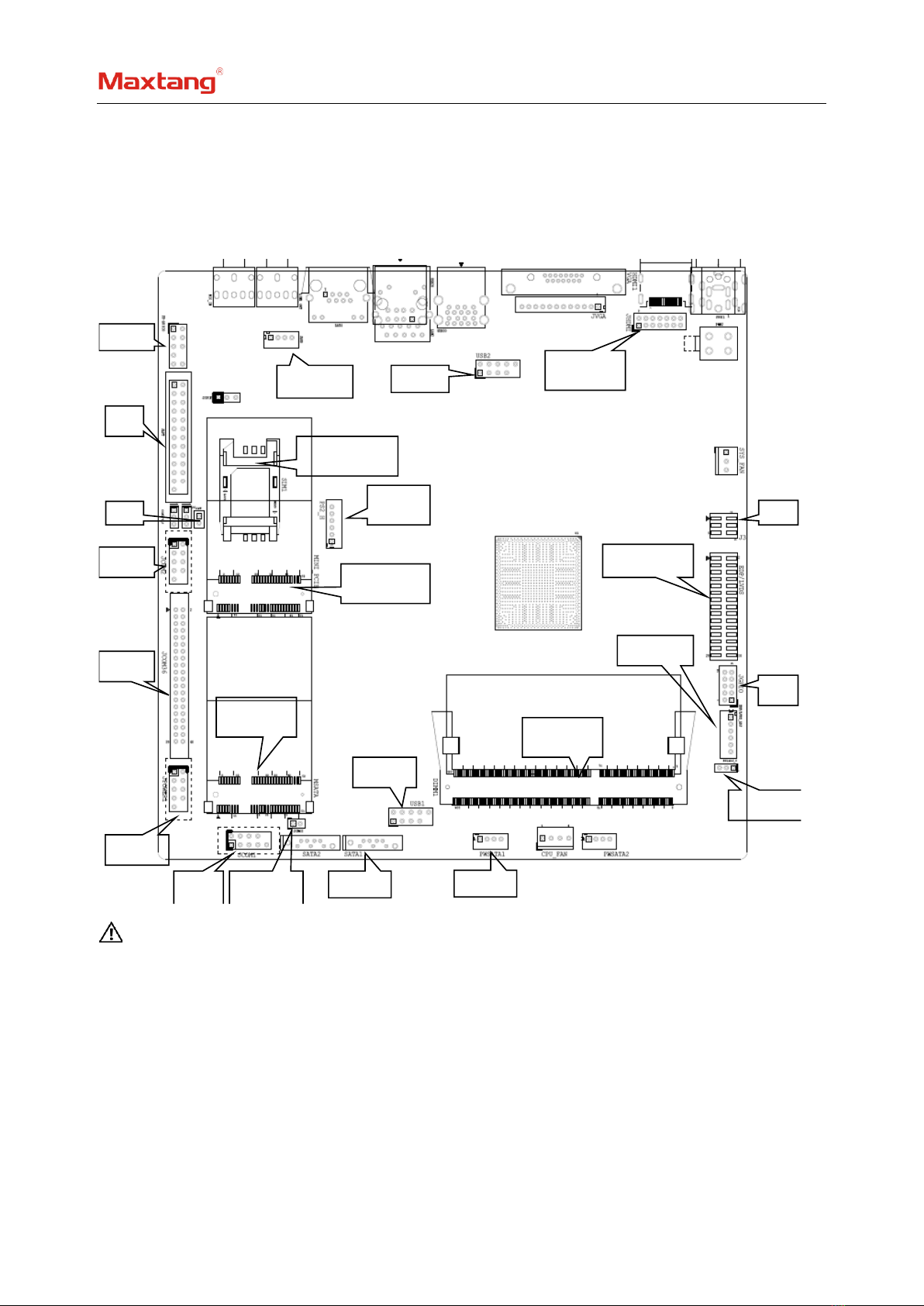
2.1 Connector Diagram................................................................................................................... 4
2.2 Jumper Setting.......................................................................................................................... 5
2.3 Memory Slots............................................................................................................................ 5
2.4 Internal Display Interface (JHDMI, JVGA) ................................................................................. 5
2.5 LVDS .......................................................................................................................................... 5
2.6 eDP (optional)........................................................................................................................... 7
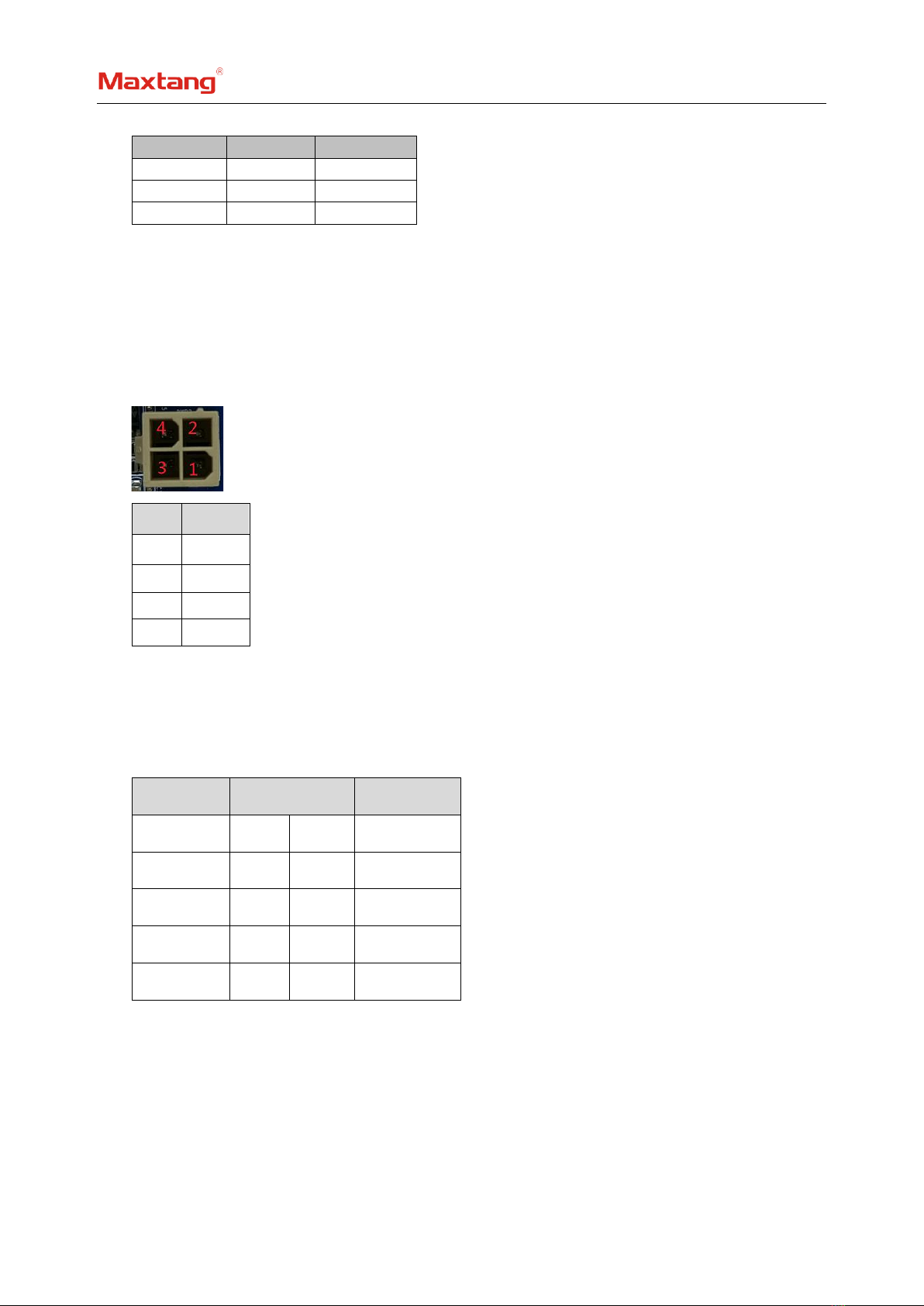
2.7 Internal PWR2........................................................................................................................... 8
2.8 Internal USB interface (USB1, USB2) ........................................................................................ 8
2.9 LAN............................................................................................................................................ 8
2.10 Audio (FP_AUDIO, JAUD, JSPIF) .............................................................................................. 9
2.11 COM (JCOM1, JCOM2, JCOM36, JCOM2/4_P) ..................................................................... 10
2.12 LPT (JLPT, J4) ......................................................................................................................... 12
2.13 GPIO(JGPIO)....................................................................................................................... 13
2.14 SATA and mSATA (SATA1, SATA2, mSATA, PWSATA1, PWSATA2) ........................................... 13
2.15 Mini-PCIe (Mini-PCIe, SIM1) ................................................................................................. 14
2.16 PS/2 (PS2).............................................................................................................................. 14
2.17 CPU FAN (CPU_FAN1) ........................................................................................................... 14
2.18 System FAN (SYS_FAN).......................................................................................................... 14
2.19 Front Panel Control Interface (JPOWER1) ............................................................................ 15
2.20 Auto Power On (JAT) ............................................................................................................. 15
2.21 CMOS Clearance/Retention (screen printing: JCMOS)......................................................... 15

Shenzhen Maxtang Computer Co., Ltd
3
Chapter 1 Product Introduction
1.1 Parameters
Processor:
Intel Bay Trail-D Celeron J1900(2.0GHz, quad-core, TDP10W)
Intel Bay Trail-D Celeron J1800(2.41GHz, dual-core, TDP10W)
Intel Bay Trail-D Atom-E3845(1.91GHz, quad-core, TDP10W)
Memory: 1x Single Channel DDR3L 1333MHz slot, up to 8GB
GPU: Integrated Intel HD graphics, supports dual display via HDMI, VGA, LVDs/eDP (dual channel 24bit LVDs, 2
lanes eDP optional)
Storage: 2 x SATA2.0, 1 x mSATA slot (SATA2 and mSATA are alternatives), 1 x eMMC (optional choice, applies to
board version 5.0 and above).
USB: Maximum of 8xUSB (two USB2.0 ports are alternatives with a LAN port).
Ethernet: Maximum of 2xLAN (LAN2 and 2 x USB2.0 are alternatives)
Audio: high-definition audio codec ALC662, supports speaker-out, Mic-in (rear port), SPDIF and power amplifier
I/O: IT8786E onboard, the board supports 6 x COM (COM6 can be set as RS232 or RS485) and 1 x LPT (can be set as
16 x GPIO). The IT8772E only supports COM1.
Other I/O: 1 x mini-PCIe (supports WIFI, support 3G/4G with SIM card slot), 8 x GPIO, PS/2 for KB /MS. The mSATA
slot can be configured as mini-PCIe slot, supports a maximum of two mini-PCIe devices.
Dimension: 170mm x 170mm
Power: 12V DC-in (Do not power the board with other voltage adapters or other power supply)
Working Temperature: -20℃~60℃

Shenzhen Maxtang Computer Co., Ltd
4
Chapter 2 Hardware
2.1 Connector Diagram
Please read the user manual carefully, before you connect to an external connector, in case of board damage.
JHDMI
Mini-PCIE
SIM CARD
Speaker
F-AUDIO
PS/2
mSATA
USB2.0
DIMM
COM3-6
JAT
eDP/LVDS
LPT
COM2
COM1
JPOWER
USB2.0
CLR_CMOS
SATA2.0
GPIO
LVDS_ADJ
BKLADJ_C
J3
PSATA

Shenzhen Maxtang Computer Co., Ltd
5
2.2 Jumper Setting
Please configure the jumpers according to your needs before installing the hardware.
How to identify the first header of jumpers and pins: Observe the mark beside the jumper or pins and find the
header marked by “1” or bold line or triangular symbol. Or observe the rear panel and the header with a
square solder pad is the first header.
2.3 Memory Slots
On-board 1x SO-DIMM DDR3L-1333MHz up to 8GB.
2.4 Internal Display Interface (JHDMI, JVGA)
The VGA and HDMI headers (optional) have been reserved on the board as a backup option. These headers
differentiate from the standard ports on the back and connect to be used at the same time.
JHDMI:
Signal
Pin
Signal
HDMI_DATA2_P
1
2
HDMI_DATA2_N
HDMI_DATA1_P
3
4
HDMI_DATA1_N
HDMI_DATA0_P
5
6
HDMI_DATA0_N
HDMI_CLK_P
7
8
HDMI_CLK_N
HDMI_SCL
9
10
HDMI_SDA
VGA_DATA_5V
11
12
GND
HDMI_DETECT
13
14
GND
JVGA:
Pin
Signal
1
CRT_DDC_ DATA
2
CRT_DDC_ CLK
3
GND
4
VGA_B_R
5
GND
6
VGA_G_R
7
GND
8
VGA_R_R
9
GND
10
CRT_HSYNC1
11
CRT_VSYNC1
12
(NC)
2.5 LVDS
Supports dual channel 24bit LVDS interface.
The power supply of the LVDS screen is controlled by the J3 jumper. The EDP/LVDS_ADJ is the screen backlight
brightness control socket, and BKLADJ_C is the screen backlight two-way adjustment control jumper.

Shenzhen Maxtang Computer Co., Ltd
6
LVDS data pin (screen printing: EDP/LVDS)
Signal
Pin
Signal
VCC
1
2
VCC
VCC
3
4
GND
GND
5
6
GND
A_DATA0_DN
7
8
A_DATA0_DP
A_DATA1_DN
9
10
A_DATA1_DP
A_DATA2_DN
11
12
A_DATA2_DP
GND
13
14
GND
A_CLK_DN
15
16
A_CLK_DP
A_DATA3_DN
17
18
A_DATA3_DP
B_DATA0_DN
19
20
B_DATA0_DP
B_DATA1_DN
21
22
B_DATA1_DP
B_DATA2_DN
23
24
B_DATA2_DP
GND
25
26
GND
B_CLK_DN
27
28
B_CLK_DP
B_DATA3_DN
29
30
B_DATA3_DP
LVDS backlight (screen printing: LVDS_ADJ)
Pin
Signal
1
GND
2
GND
3
LCD_BKL_ADJ
4
LCD_BKL_ON
5
12V
6
12V
LVDS screen backlight two-way adjustment jumper (screen printing: BKLADJ_C)
Pin
Setting
Function
1-2
Close
Backlight controls reverse
2-3
Close
Backlight controls standard

Shenzhen Maxtang Computer Co., Ltd
7
LVDS screen voltage jumper (screen printing: J3)
Pin
Setting
Function
1-2
Close
VCC(+3.3V)
3-4
Close
VCC(+5V)
5-6
Close
VCC(+12V)
Note: The LVDS display power supply can be adjusted among 12V/5V/3.3V via jumper setting. Users can
connect the VCC with a jumper cap by 2pin according to their LVDS screen’s voltage (Short-circuiting two or
more interfaces via jumper cap at the same time is strictly forbidden).
2.6 eDP (optional)
The board supports an optional eDP interface (2 lanes). When it is set as eDP the LVDs function will be
disabled. The J3 jumper controls the screen power supply and the EDP/LVDS_ADJ controls the screen backlight
brightness.
eDP data pin (screen printing: EDP/LVDS)
Signal
Pin
Signal
VCC
1
2
VCC
VCC
3
4
EDP_HPD
GND
5
6
GND
EDP_AUXN
7
8
EDP_AUXP
(NC)
9
10
(NC)
EDP_DATA0_P
11
12
EDP_DATA0_N
GND
13
14
GND
(NC)
15
16
(NC)
EDP_DATA1_P
17
18
EDP_DATA1_N
(NC)
19
20
(NC)
(NC)
21
22
(NC)
(NC)
23
24
(NC)
GND
25
26
GND
(NC)
27
28
(NC)
(NC)
29
30
(NC)
eDP backlight brightness adjustment pin (Screen printing: EDP/LVDS_ADJ)
Pin
Signal
1
GND
2
GND
3
LCD_BKL_ADJ
4
LCD_BKL_ON
5
12V
6
12V

Shenzhen Maxtang Computer Co., Ltd
8
eDP voltage pin (Screen printing: J3)
Interface
Settings
Function
1-2
Close
VCC(+3.3V)
3-4
Close
VCC(+5V)
5-6
Close
VCC(+12V)
Note: The eDP display power is controlled by jumpers. The voltage can be adjusted between 12V/5V/3.3V.
Don't short-circuit two or more interfaces with a jumper cap.
2.7 Internal PWR2
This power socket can be used as the power input of the motherboard, or as a power output socket to supply
power to the peripheral devices (the voltage is the same as the input voltage of the motherboard PWR1).
Pin
Signal
1
GND
2
GND
3
+12V
4
+12V
2.8 Internal USB interface (USB1, USB2)
The internal USB headers are USB2.0 interface.
USB1, USB2:
Signal
Pin
Signal
5V
1
2
5V
USB DATA-
3
4
USB DATA-
USB DATA+
5
6
USB DATA+
GND
7
8
GND
9
10
NC
2.9 LAN
The board features 2xRJ45 interfaces RTL8111H Gigabit Ethernet controllers.
One of the LAN ports (RJ45 interface, screen printing “LAN2”) can be changed to two USB2.0.
Both ports support Wake on LAN (The situation where the board reconnects with DC power after it cuts off
DC power is not included). One of the LANs (Screen printing “LAN1”) supports PXE network boot.

Shenzhen Maxtang Computer Co., Ltd
9
RJ45 LAN LED Description:
LILED (Orange)Status
Function
ACTLED (Green) Status
Function
Always on
Connected
Blink
Data transmission
2.10 Audio (FP_AUDIO, JAUD, JSPIF)
Features the ALC662 audio codec, the green interface is Speaker-out and the pink interface is Mic-in; the JAUD
is amplifier output; the JSPIF is SPDIF-out.
FP_AUDIO:
Signal
Pin
Signal
MIC2-L
1
2
AGND
MIC2-R
3
4
AVCC
FRO-R
5
6
MIC2-JD
F-IO-SEN(AGNG)
7
8
(NC)
FRO-L
9
10
LIN2-JD
JAUD:
Pin
Signal
1
L+
2
L-
3
R-
4
R+
JSPIF:
Pin
Signal
1
+5V
2
SPDIF Out
3
GND

Shenzhen Maxtang Computer Co., Ltd
10
2.11 COM (JCOM1, JCOM2, JCOM36, JCOM2/4_P)
Supports 6 x RS232, and COM6 can be set as RS485.
COM1 and COM2 are industrial definitions.
COM2 and COM4 come with power and can set up a different voltage through jumper COM2/4_P.
JCOM1:
Signal
Pin
Signal
DCD#
1
2
DSR#
RXD
3
4
RTS#
TXD
5
6
CTS#
DTR#
7
8
RI#
GND
9
10
JCOM2:
Signal
Pin
Signal
DCD#
1
2
DSR#
RXD
3
4
RTS#
TXD
5
6
CTS#
DTR#
7
8
(NC) / VCC(5V/12V)
GND
9
10
JCOM2/4 voltage setting(screen printing:COM2/4_P)
Signal
Pin
Signal
1-2
Close
VCC_12V
2-3
Close
VCC-5V
Do not connect three sets of COM at the same time in case of board damages.
JCOM36:
Signal
Pin
Signal
DCD#_3
1
2
RXD_3
TXD_3
3
4
DTR#_3
GND
5
6
DSR#_3
RTS#_3
7
8
CTS#_3

Shenzhen Maxtang Computer Co., Ltd
11
Signal
Pin
Signal
RI#_3
9
10
(NC)
DCD#_4
11
12
RXD_4
TXD_4
13
14
DTR#_4
GND
15
16
DSR#_4
RTS#_4
17
18
CTS#_4
(NC) / VCC(5V/12V)
19
20
(NC)
DCD#_5
21
22
RXD_5
TXD_5
23
24
DTR#_5
GND
25
26
DSR#_5
RTS#_5
27
28
CTS#_5
RI#_5
29
30
(NC)
DCD#_6
31
32
RXD_6
TXD_6
33
34
DTR#_6
GND
35
36
DSR#_6
RTS#_6
37
38
CTS#_6
RI#_6
39
40
(NC)
When COM6 is set as RS232 and RS485, the header definition is as follows:
Pin
RS232
RS485
1
DCD#
DATA-
2
RXD
DATA+
3
TXD
(NC)
4
DTR#
(NC)
5
GND
GND
6
DSR#
(NC)
7
RTS#
(NC)
8
CTS#
(NC)
9
RI#
(NC)

Shenzhen Maxtang Computer Co., Ltd
12
2.12 LPT (JLPT, J4)
The board provides a set of 2x13pin LPT header (space in between: 2.0mm). Users can use it to connect to
other equipment like a printer. Users need to disable the LPT function in the BIOS to set the LPT as 16 lanes GIPO.
When the JLPT pin is set for different functions, the J4 as a voltage configuration pin is also required to change.
JLPT (Printing port):
Signal
Pin
Signal
STB
1
2
AFD
LPT_ PPD0
3
4
ERROR
LPT_ PPD1
5
6
INIT
LPT_ PPD2
7
8
SLIN
LPT_ PPD3
9
10
GND
LPT_ PPD4
11
12
GND
LPT_ PPD5
13
14
GND
LPT_ PPD6
15
16
GND
LPT_ PPD7
17
18
GND
ACK
19
20
GND
BUSY
21
22
GND
PE
23
24
GND
SLCT
25
26
(NC)
JLPT(GPIO):
Signal
Pin
Signal
GPIO_87
1
2
GPIO_86
GPIO_70
3
4
(NC)
GPIO_71
5
6
GPIO_85
GPIO_72
7
8
GPIO_84
GPIO_73
9
10
GND
GPIO_74
11
12
GND
GPIO_75
13
14
GND

Shenzhen Maxtang Computer Co., Ltd
13
GPIO_76
15
16
GND
GPIO_77
17
18
GND
GPIO_83
19
20
GND
GPIO_82
21
22
GND
GPIO_81
23
24
GND
GPIO_80
25
26
(NC)
J4 (Voltage setting):
Function
Setting
GPIO
short-circuit 1-2
Printing
short-circuit 2-3
Do not short-circuit three sets of pins same time in case of board damages.
2.13 GPIO(JGPIO)
A set of 2×5Pin (connected from CPU) JGPI0 header, 8 programmable I/O interfaces in total.
Signal
Pin
Signal
GPI_S5_0
1
2
1.8V
GPI_S5_1
3
4
GPO_S5_6
GPI_S5_2
5
6
GPO_S5_7
GPI_S5_3
7
8
GPO_S5_8
GND
9
10
GPO_S5_9
2.14 SATA and mSATA (SATA1, SATA2, mSATA, PWSATA1, PWSATA2)
Maximum of two standard SATA2.0 interfaces (SATA2 and mSATA are alternatives), one mSATA slot, and two
4pin SATA power supply sockets.
PWSATA1/2:
Pin
Signal
1
+5V
2
GND
3
GND

Shenzhen Maxtang Computer Co., Ltd
14
4
+12V
2.15 Mini-PCIe (Mini-PCIe, SIM1)
Supports Wi-Fi card with standard SIM card slot for 3G/4G module expansions.
2.16 PS/2 (PS2)
The board offers a 6Pin PS/2 socket.
Pin
Signal
1
+5V
2
KB_DATA
3
KB_CLK
4
MS_ DATA
5
MS_CLK
6
GND
2.17 CPU FAN (CPU_FAN1)
The board offers a 4Pin CPU smart fan socket. The default power voltage setting is 5V (12V optional).
CPU_FAN:
Pin
Signal
1
GND
2
VCC
3
CPUFAN_TAC
4
CPUFAN_CTL
2.18 System FAN (SYS_FAN)
The board offers a 3Pin system fan socket, the default power voltage setting is 5V (12V optional).
SYS_FAN:
Pin
Signal
1
GND
2
VCC
3
CPUFAN_TAC

Shenzhen Maxtang Computer Co., Ltd
15
2.19 Front Panel Control Interface (JPOWER1)
The front panel control interface is intended to connect the function buttons and the light indicator on the
front panel.
JPOWER1:
Signal
Pin
Signal
HDD_LED+
1
2
PWR_LED+
HDD_LED-
3
4
PWR_LED-
RST_BTN-
5
6
PWR_ON+
RST_BTN+
7
8
PWR_ON-
(NC)
9
10
2.20 Auto Power On (JAT)
JAT:
Setting
JAT
Close
Hardware Auto Start
Note: This jumper function is similar to the “Restore AC Power Loss” function in the BIOS. When the
latter is set to be “power on” the device will start automatically after being connected to power.
2.21 CMOS Clearance/Retention (screen printing: JCMOS)
The CMOS is powered by onboard button batteries, clearing CMOS will permanently remove the previous
system settings and restore the board to the original (factory settings) system settings.
Step 1: Turn off the PC and disconnect the power.
Step 2: Use the jumper cap to connect the 1st and 2nd header of JCMOS for about 10 seconds, then
disconnect.
Step 3: Press the <Del> button to enter the BIOS after restarting the computer, load the optimal default value,
save, and exit the settings.
JCMOS:
Setting
JCMOS
Close
Clear the CMOS
Please don’t clear COMS when the PC is connected to power in case of board damages.
Other manuals for BYT60
1
Table of contents
Other Maxtang Motherboard manuals

Maxtang
Maxtang WL35 User manual

Maxtang
Maxtang KL35 User manual

Maxtang
Maxtang SKD70 User manual

Maxtang
Maxtang JSL-15 User manual

Maxtang
Maxtang WL10 User manual

Maxtang
Maxtang DTJ6412-I User manual

Maxtang
Maxtang BYT-35 User manual

Maxtang
Maxtang AL-10 User manual

Maxtang
Maxtang WL10 User manual

Maxtang
Maxtang WL35 User manual

Maxtang
Maxtang FP20 User manual

Maxtang
Maxtang SKD70 User manual

Maxtang
Maxtang BYT-35 SBC User manual

Maxtang
Maxtang FP50 User manual

Maxtang
Maxtang EHL-35 User manual

Maxtang
Maxtang MITX-KL10 User manual

Maxtang
Maxtang EHL-10 User manual

Maxtang
Maxtang BW-35 User manual

Maxtang
Maxtang TL10 User manual

Maxtang
Maxtang FP-10 User manual