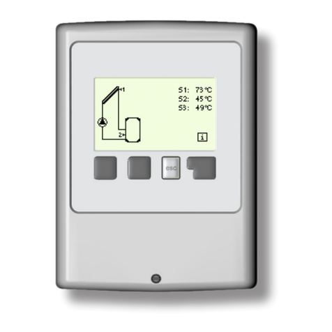
Motorola DSP56F801 Instructions for use
Other Motorola Controllers manuals

Motorola
Motorola MVME162FX User manual
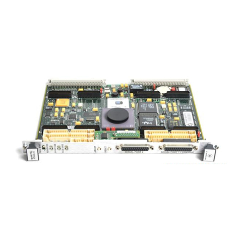
Motorola
Motorola MVME162P-344 Series Quick start guide
Motorola
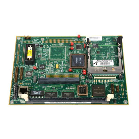
Motorola MBX Series Quick start guide
Motorola
Motorola Semiconductor MC68HC11F1 User manual
Motorola
Motorola MC68360 User manual
Motorola
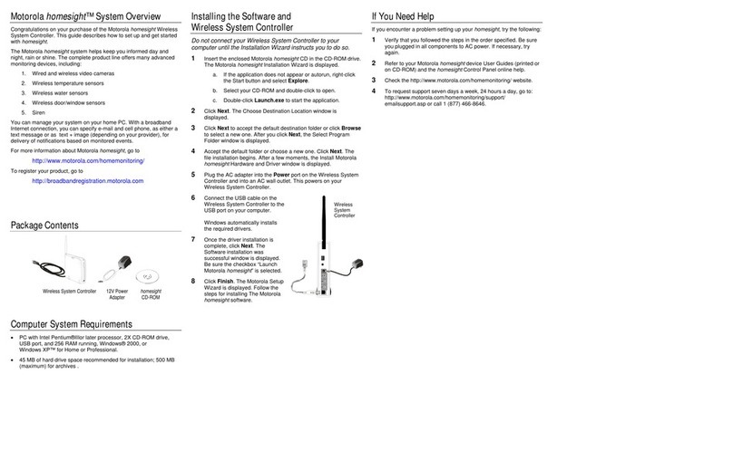
Motorola HMGW1075 User manual

Motorola
Motorola MVME162LX 300 Series Quick start guide
Motorola
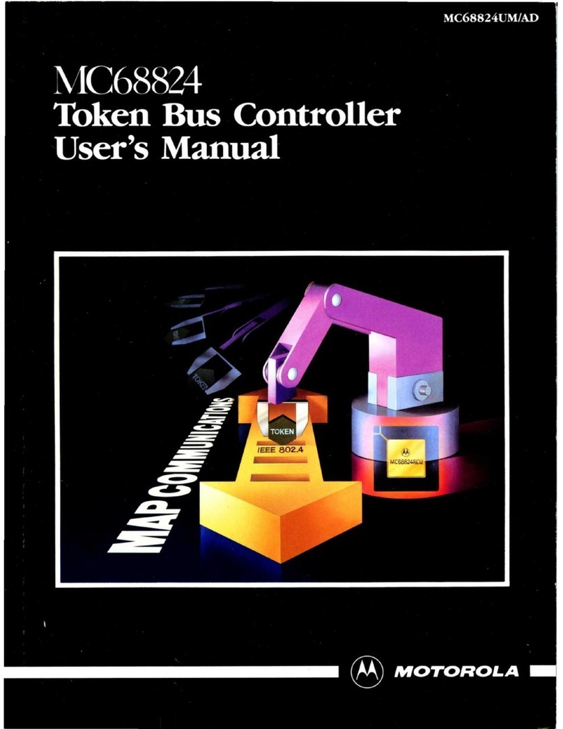
Motorola MC68824 User manual
Motorola
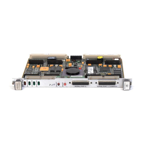
Motorola MVME172 User manual
Motorola
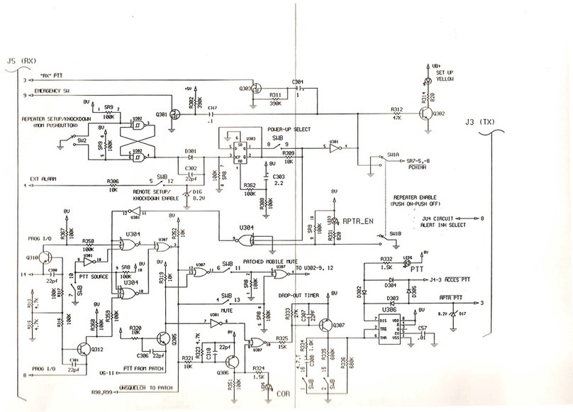
Motorola I50R Quick start guide
Motorola
Motorola M68HC08 User manual
Motorola
Motorola hmdc5025 User manual
Motorola
Motorola MVME172P4 Series User manual
Motorola
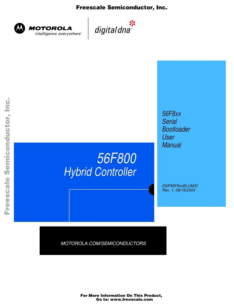
Motorola RZ100 User manual
Motorola
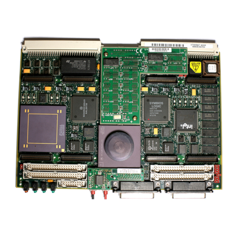
Motorola 56F800 User manual
Motorola
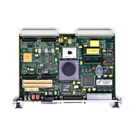
Motorola 700 Series Quick start guide
Motorola
Motorola MVME162P2 Series Quick start guide

Motorola
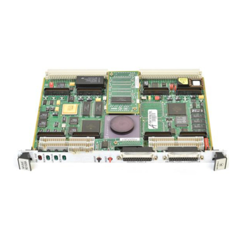
Motorola MC68360 User manual
Motorola
Motorola MVME162FX400 Series User manual
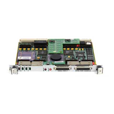
Motorola
Motorola MVME162 User manual
Popular Controllers manuals by other brands
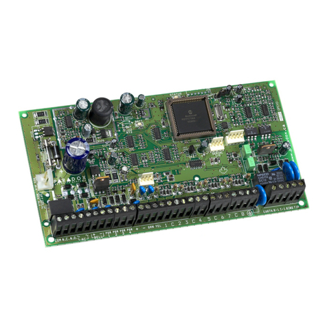
Digiplex
Digiplex DGP-848 Programming guide
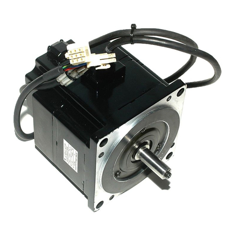
YASKAWA
YASKAWA SGM series user manual
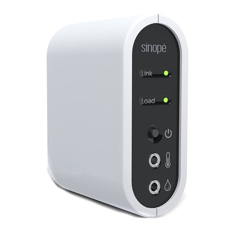
Sinope
Sinope Calypso RM3500ZB installation guide
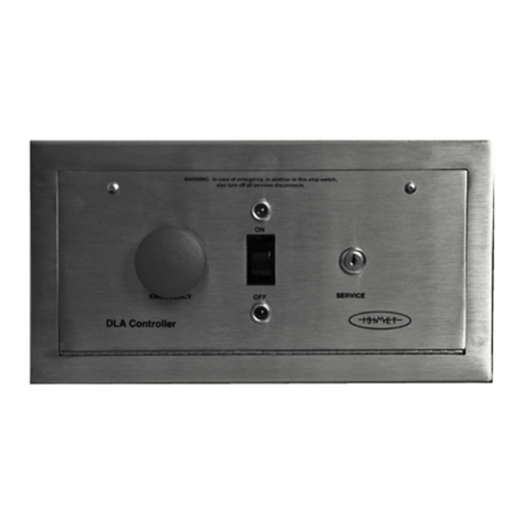
Isimet
Isimet DLA Series Style 2 Installation, Operations, Start-up and Maintenance Instructions
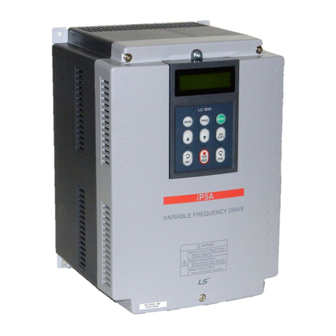
LSIS
LSIS sv-ip5a user manual
Rockwell Automation
Rockwell Automation 1769-L31 installation instructions
